Chris A Mack Fundamental Principles of Optical Lithography
- Slides: 24

Chris A. Mack, Fundamental Principles of Optical Lithography, (c) 2007 Figure 1. 1 Diagram of a simple subtractive patterning process. 1

Chris A. Mack, Fundamental Principles of Optical Lithography, (c) 2007 Figure 1. 2 Erosion of a photoresist line during etching, showing the vertical and horizontal etch rate components. 2

Chris A. Mack, Fundamental Principles of Optical Lithography, (c) 2007 Figure 1. 3 Patterning as a means of selective doping using ion implantation. 3

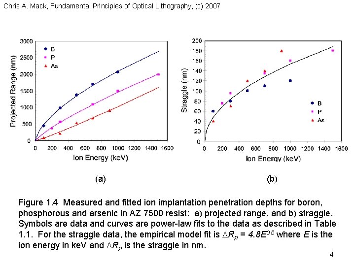
Chris A. Mack, Fundamental Principles of Optical Lithography, (c) 2007 (a) (b) Figure 1. 4 Measured and fitted ion implantation penetration depths for boron, phosphorous and arsenic in AZ 7500 resist: a) projected range, and b) straggle. Symbols are data and curves are power-law fits to the data as described in Table 1. 1. For the straggle data, the empirical model fit is DRp = 4. 8 E 0. 5 where E is the ion energy in ke. V and DRp is the straggle in nm. 4

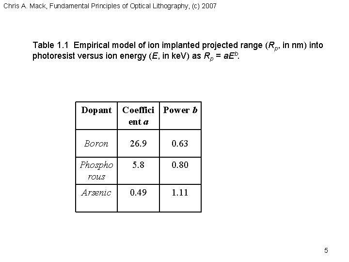
Chris A. Mack, Fundamental Principles of Optical Lithography, (c) 2007 Table 1. 1 Empirical model of ion implanted projected range (Rp, in nm) into photoresist versus ion energy (E, in ke. V) as Rp = a. Eb. Dopant Coeffici Power b ent a Boron 26. 9 0. 63 Phospho rous 5. 8 0. 80 Arsenic 0. 49 1. 11 5

Chris A. Mack, Fundamental Principles of Optical Lithography, (c) 2007 Figure 1. 5 Cross-section of a pair of CMOS transistors showing most of the layers through metal 1. 6

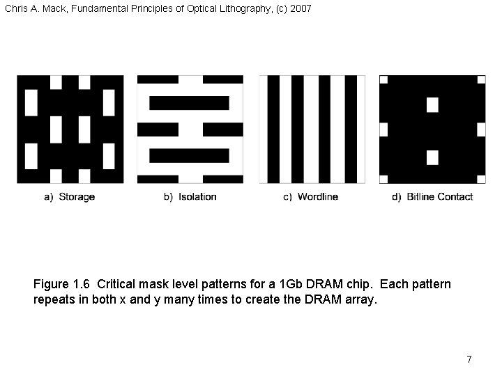
Chris A. Mack, Fundamental Principles of Optical Lithography, (c) 2007 Figure 1. 6 Critical mask level patterns for a 1 Gb DRAM chip. Each pattern repeats in both x and y many times to create the DRAM array. 7

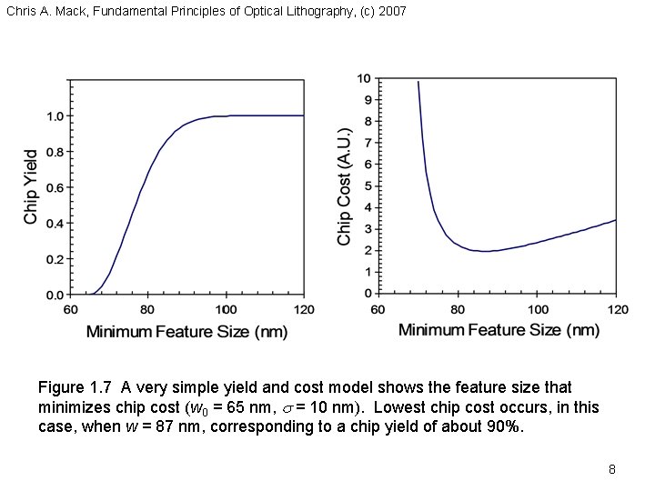
Chris A. Mack, Fundamental Principles of Optical Lithography, (c) 2007 Figure 1. 7 A very simple yield and cost model shows the feature size that minimizes chip cost (w 0 = 65 nm, s = 10 nm). Lowest chip cost occurs, in this case, when w = 87 nm, corresponding to a chip yield of about 90%. 8

Chris A. Mack, Fundamental Principles of Optical Lithography, (c) 2007 Figure 1. 8 Example fab profit curve using the yield and cost models of Figure 1. 7 and assuming the value of the chip is inversely proportional to the minimum feature size. For this example, maximum profit occurs when w = 80 nm, even though the yield is only 65%. 9

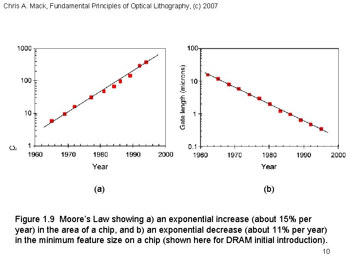
Chris A. Mack, Fundamental Principles of Optical Lithography, (c) 2007 (a) (b) Figure 1. 9 Moore’s Law showing a) an exponential increase (about 15% per year) in the area of a chip, and b) an exponential decrease (about 11% per year) in the minimum feature size on a chip (shown here for DRAM initial introduction). 10

Chris A. Mack, Fundamental Principles of Optical Lithography, (c) 2007 Figure 1. 10 Moore’s Law showing an exponential increase in the number of transistors on a semiconductor chip over time (shown here for DRAM initial introduction). 11

Chris A. Mack, Fundamental Principles of Optical Lithography, (c) 2007 Figure 1. 11 Example of a typical sequence of lithographic processing steps, illustrated for a positive resist. 12

Chris A. Mack, Fundamental Principles of Optical Lithography, (c) 2007 Figure 1. 12 Iconic representation of the integration of the various lithographic process steps into a photolithography cell. Many steps, such as chill plates after the bake steps, have been omitted. 13

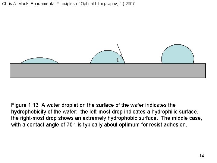
Chris A. Mack, Fundamental Principles of Optical Lithography, (c) 2007 Figure 1. 13 A water droplet on the surface of the wafer indicates the hydrophobicity of the wafer: the left-most drop indicates a hydrophilic surface, the right-most drop shows an extremely hydrophobic surface. The middle case, with a contact angle of 70 , is typically about optimum for resist adhesion. 14

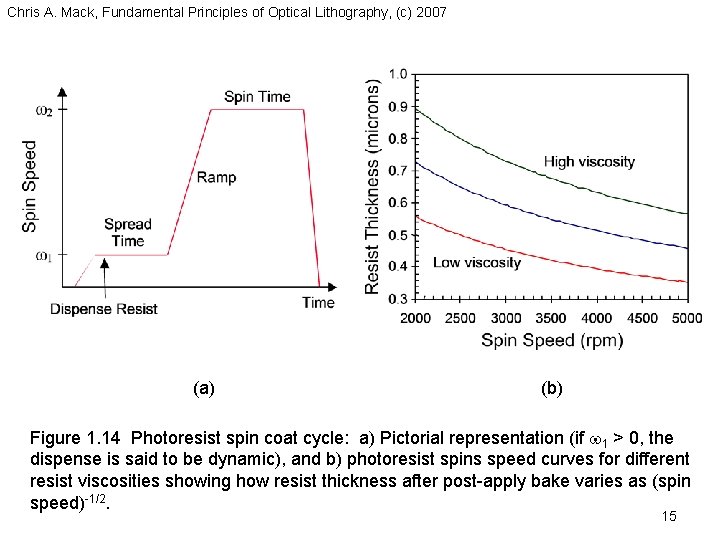
Chris A. Mack, Fundamental Principles of Optical Lithography, (c) 2007 (a) (b) Figure 1. 14 Photoresist spin coat cycle: a) Pictorial representation (if w 1 > 0, the dispense is said to be dynamic), and b) photoresist spins speed curves for different resist viscosities showing how resist thickness after post-apply bake varies as (spin speed)-1/2. 15

Chris A. Mack, Fundamental Principles of Optical Lithography, (c) 2007 Figure 1. 15 A balance of spin-coat forces at the wafer edge leads to the formation of a resist edge bead. 16

Chris A. Mack, Fundamental Principles of Optical Lithography, (c) 2007 Figure 1. 16 Lithographic printing in semiconductor manufacturing has evolved from contact printing (in the early 1960 s) to projection printing (from the mid 1970 s to today). 17

Chris A. Mack, Fundamental Principles of Optical Lithography, (c) 2007 Figure 1. 17 Scanners and steppers use different techniques for exposing a large wafer with a small image field. 18

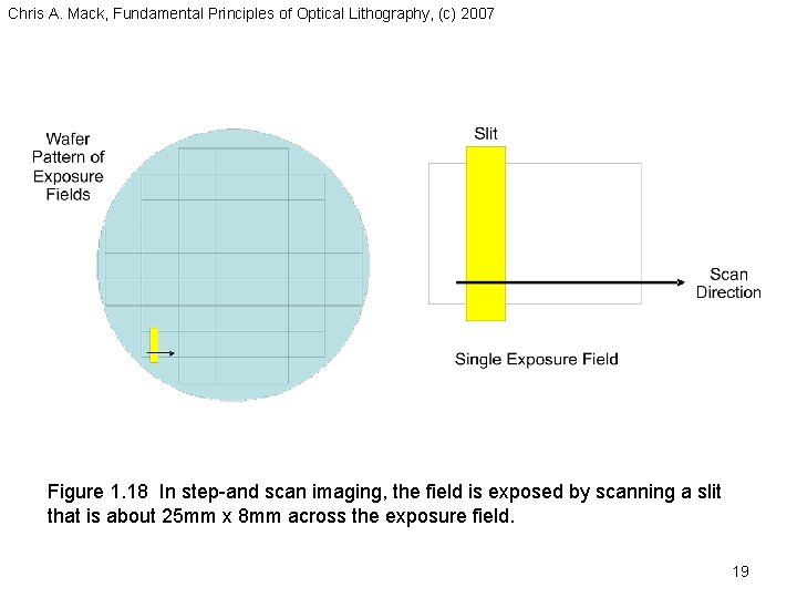
Chris A. Mack, Fundamental Principles of Optical Lithography, (c) 2007 Figure 1. 18 In step-and scan imaging, the field is exposed by scanning a slit that is about 25 mm x 8 mm across the exposure field. 19

Chris A. Mack, Fundamental Principles of Optical Lithography, (c) 2007 Figure 1. 19 The progression of l/NA of lithographic tools over time (year of first commercial tool shipment). 20

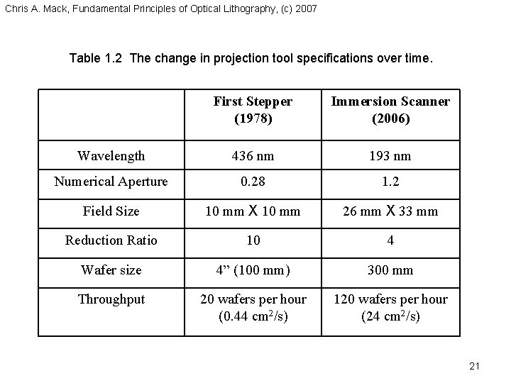
Chris A. Mack, Fundamental Principles of Optical Lithography, (c) 2007 Table 1. 2 The change in projection tool specifications over time. First Stepper (1978) Immersion Scanner (2006) Wavelength 436 nm 193 nm Numerical Aperture 0. 28 1. 2 Field Size 10 mm X 10 mm 26 mm X 33 mm Reduction Ratio 10 4 Wafer size 4” (100 mm) 300 mm Throughput 20 wafers per hour (0. 44 cm 2/s) 120 wafers per hour (24 cm 2/s) 21

Chris A. Mack, Fundamental Principles of Optical Lithography, (c) 2007 Figure 1. 20 Photoresist pattern on a silicon substrate (i-line exposure pictured here) showing prominent standing waves. 22

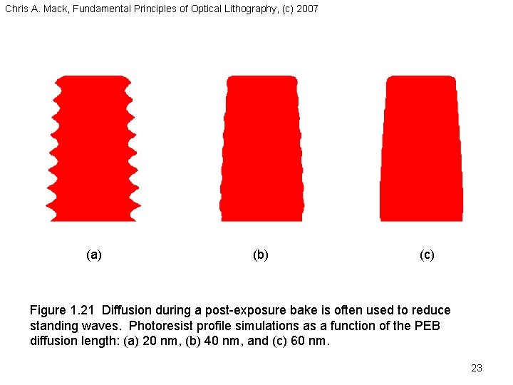
Chris A. Mack, Fundamental Principles of Optical Lithography, (c) 2007 (a) (b) (c) Figure 1. 21 Diffusion during a post-exposure bake is often used to reduce standing waves. Photoresist profile simulations as a function of the PEB diffusion length: (a) 20 nm, (b) 40 nm, and (c) 60 nm. 23

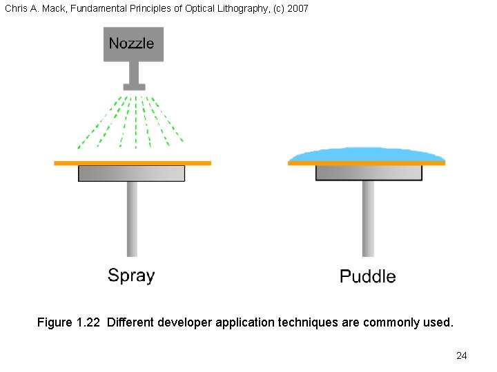
Chris A. Mack, Fundamental Principles of Optical Lithography, (c) 2007 Figure 1. 22 Different developer application techniques are commonly used. 24