NANOSCALE LITHOGRAPHY TECHNIQUES AND TECHNOLOGY EE 4611 DEHUA


 is manipulation of matter on an atomic, molecular, and supramolecular")


 is the practice of")


- Slides: 29
NANOSCALE LITHOGRAPHY, TECHNIQUES AND TECHNOLOGY EE 4611 DEHUA LIU 4/8/2016
• THE origin of Nanoscale Lithography • Major methods of Nanoscale Lithography • Advantages and disadvantages of different methods of Nanoscale Lithography
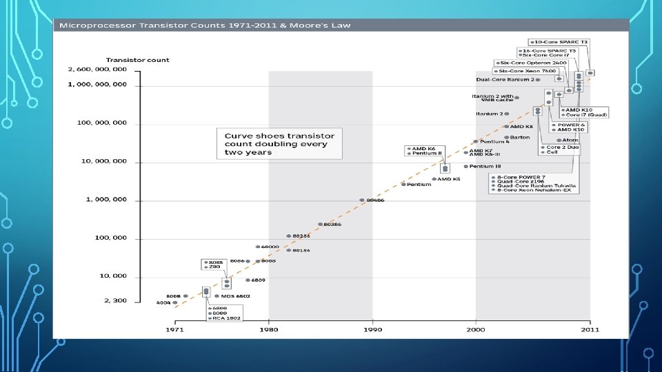
MOORE’S LAW SMALLER, FASTER, CHEAPER HTTP: //NANOLITHOGRAPHY. SPIEDIGITALLIBRARY. ORG/ARTICLE. ASPX? ARTICLEID=1166831
NANOSCALE TECHNOLOGY • A branch of nanotechnology in which standard size tools are used to manufacture simple structures and devices with dimensions on the order of a few nanometer s or less, where one nanometer (1 nm) is equal to a billionth of a meter (10 -9 m). • For better recognize size of 1 nm, It is the equivalent of one hundred thousandth of a single hair • whatis. techtarget. com/definition/na noscale-technology
• Nanotechnology ("nanotech") is manipulation of matter on an atomic, molecular, and supramolecular scale. The earliest, widespread description of nanotechnology referred to the particular technological goal of precisely manipulating atoms and molecules for fabrication of macroscale products, also now referred to as molecular nanotechnology. A more generalized description of nanotechnology was subsequently established by the National Nanotechnology Initiative, which defines nanotechnology as the manipulation of matter with at least one dimension sized from 1 to 100 nanometers. This definition reflects the fact that quantum mechanical effects are important at this quantum-realm scale, and so the definition shifted from a particular technological goal to a research category inclusive of all types of research and technologies that deal with the special properties of matter that occur below the given size threshold. It is therefore common to see the plural form "nanotechnologies" as well as "nanoscale technologies" to refer to the broad range of research and applications whose common trait is size. Because of the variety of potential applications (including industrial and military), governments have invested billions of dollars in nanotechnology research. Until 2012, through its National Nanotechnology Initiative, the USA has invested 3. 7 billion dollars, the European Union has invested 1. 2 billion and Japan 750 million dollars. • Nanotechnology as defined by size is naturally very broad, including fields of science as diverse as surface science, organic chemistry, molecular biology, semiconductor physics, microfabrication, etc. The associated research and applications are equally diverse, ranging from extensions of conventional device physics to completely new approaches based upon molecular self-assembly, from developing new materials with dimensions on the nanoscale to direct control of matter on the atomic scale. • https: //en. wikipedia. org/wiki/Nanotechnology
MISUNDERSTANDING ABOUT NANOSCALE TECHNOLOGY • If Nano material has not special structure or function, it could not be called nanoscale technology. Nanoscale technology is scientists and engineer arrange molecules or atoms on Nano material’s surface to design a specific structure to make it functional.
WHAT DOES NANOSCALE TECHNOLOGY BRING TO US
HTTP: //WWW. ODDITYCENTRAL. COM/NEWS/STUDENT-CREATES-HYDROPHOBIC-SHIRT-THATS-IMPOSSIBLE-TO-STAIN. H
HTTP: //CHICAGOINNO. STREETWISE. CO/2015/02/11/NISSAN-LEAF-PAINT-TECHNOLOGY-AT-THE-CHICAGO-AUTO-SHOW/
HTTPS: //SITES. GOOGLE. COM/A/DEPAUL. EDU. IN/DE-PAUL-TIMES/OCTOBER-2008 -PUBLICATION/NANOROBOTICS
NANO MANUFACTURING SCIENCE • Is the base of Nanoscale Technology, through designing Nano graphics to produce functional Nano materials. There are two main methods producing Nano graphics: • 1. Modern chemical technology: Atomic layer epitaxy; Plasma enhanced • Chemical vapor deposition; Metal organic chemical vapor deposition; Molecular beam epitaxy • 2. Nanoscale Lithography • http: //www. cqvip. com/qk/92621 b/200503/20087550. html
LITHOGRAPHY • Lithography (from Ancient Greek λίθος, lithos, meaning "stone", and γράφειν, graphein, meaning "to write") is a method of printing originally based on the immiscibility of oil and water. The printing is from a stone (lithographic limestone) or a metal plate with a smooth surface. • • https : //en. wikipedia. org/wiki/Lithography
https: //www. google. com/imgres? imgurl=http: //s. hswstatic. com/gif/sl-443. jpg&imgrefurl=http: //entertainment. howstuffworks. com/arts/artwork/stonelithography. htm&h=347&w=400&tbnid=GIl. LGp. IFVUCV 1 M: &tbnh=160&tbnw=184&docid=V_w 9 JSyw. Z 8 ggo. M&itg=1&usg=__Em. Qz 0 A 0 n. Hz. DRn. CBYOAq 0 ol. Mp. Xq. A=&sa=X&ved=0 ah. UKEwivjfv. Dn. P_LAh. Wqto. MK HUPMBn. YQ 9 QEIIz. AA#h=347&tbnh=160&tbnw=184&w=400
NANOSCALE LITHOGRAPHY • Nanolithography is the branch of nanotechnology concerned with the study and application of fabricating nanometer-scale structures, meaning patterns with at least one lateral dimension between 1 and 100 nm.
NANOSCRIBE/ HTTPS: //SIMOTRON. WORDPRESS. COM/2013/03/22/NANOSCALE-3 D-PRINTED-MICROSTRUCTURES-BY-
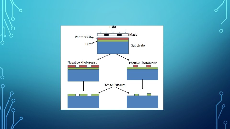
PHOTOLITHOGRAPHY • Photolithography, also termed optical lithography or UV lithography, is a process used in microfabrication to pattern parts of a thin film or the bulk of a substrate. It uses light to transfer a geometric pattern from a photomask to a light-sensitive chemical "photoresist", or simply "resist, " on the substrate. A series of chemical treatments then either engraves the exposure pattern into, or enables deposition of a new material in the desired pattern upon, the material underneath the photo resist. • Projection Printing Technique • Limited by diffraction limit
• A photoresist is a light-sensitive material used in several industrial processes, such as photolithography and photoengraving, to form a patterned coating on a surface. • A positive resist is a type of photoresist in which the portion of the photoresist that is exposed to light becomes soluble to the photoresist developer. The portion of the photoresist that is unexposed remains insoluble to the photoresist developer. • A negative resist is a type of photoresist in which the portion of the photoresist that is exposed to light becomes insoluble to the photoresist developer. The unexposed portion of the photoresist is dissolved by the photoresist developer.
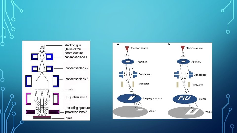
ELECTRON-BEAM LITHOGRAPHY • Electron-beam lithography (often abbreviated as e-beam lithography) is the practice of scanning a focused beam of electrons to draw custom shapes on a surface covered with an electron-sensitive film called a resist ("exposing"). The electron beam changes the solubility of the resist, enabling selective removal of either the exposed or non-exposed regions of the resist by immersing it in a solvent ("developing"). • Allows accuracy down to as small as 10 nm dimensions • highly accurate and reliable pattern writing
PROXIMITY EFFECT • The smallest features produced by electron-beam lithography have generally been isolated features, as nested features exacerbate the proximity effect, whereby electrons from exposure of an adjacent region spill over into the exposure of the currently written feature, effectively enlarging its image, and reducing its contrast
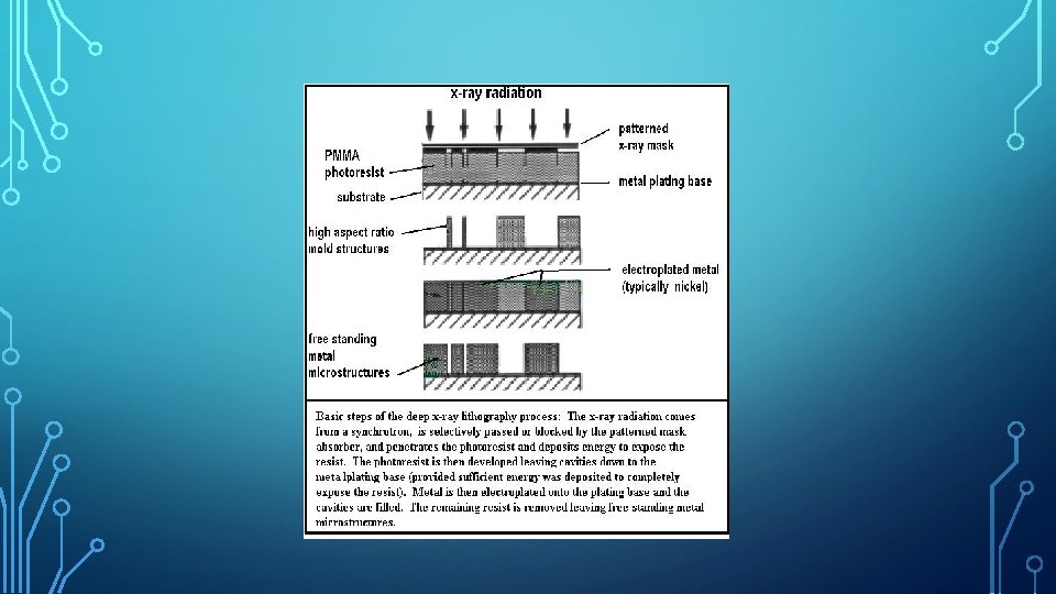
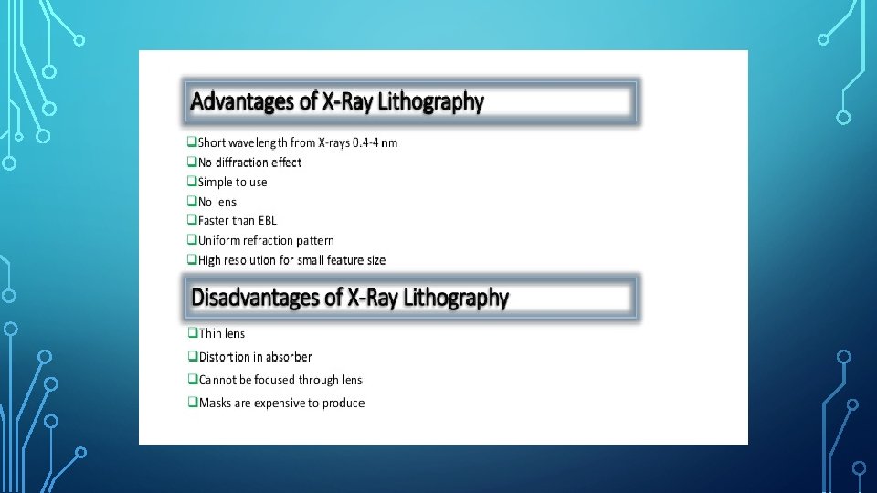
X-RAY LITHOGRAPHY • X-ray lithography, is a process used in electronic industry to selectively remove parts of a thin film. It uses X-rays to transfer a geometric pattern from a mask to a light-sensitive chemical photoresist, or simply "resist, " on the substrate. A series of chemical treatments then engraves the produced pattern into the material underneath the photoresist. • Allowing smaller feature sizes. Having short wavelengths (below 1 nm), X-rays overcome the diffraction limits of optical lithography
CONCLUSION Source Form Disadvantages Advantages Photolithography UV Light Projection Printing Limited by UV Wavelength Cheap Electron-beam lithography focused beam of electrons Direct Writing Expensive Highly Accurate X-Ray Lithography X-Ray Proximity Printing Expensive/Fragil e Masks Accurate/Efficient Fast
REFERENCES • HTTP: //NANOLITHOGRAPHY. SPIEDIGITALLIBRARY. ORG/ARTICLE. ASPX? ARTICLEID=1166831 • whatis. techtarget. com/definition/nanoscale-technology • https: //en. wikipedia. org/wiki/Nanotechnology • HTTP: //CHICAGOINNO. STREETWISE. CO/2015/02/11/NISSAN-LEAF-PAINT-TECHNOLOGY-AT-THE-CHICAGO-AUTO-SHOW / • HTTPS: //SITES. GOOGLE. COM/A/DEPAUL. EDU. IN/DE-PAUL-TIMES/OCTOBER-2008 -PUBLICATION/NANOROBOTICS • http: //www. cqvip. com/qk/92621 b/200503/20087550. html • https: //en. wikipedia. org/wiki/Lithography • https: //www. google. com/imgres? imgurl=http: //s. hswstatic. com/gif/sl-443. jpg&imgrefurl=http: //entertainment. howstuffworks. com/arts/artwork/stonelithography. htm&h=347&w=400&tbnid=GIl. LGp. IFVUCV 1 M: &tbnh=160&tbnw=184&docid=V_w 9 JSyw. Z 8 ggo. M&itg=1&usg=__Em. Qz 0 A 0 n. Hz. DRn. CBYOAq 0 ol. Mp. Xq. A=& sa=X&ved=0 ah. UKEwivjfv. Dn. P_LAh. Wqto. MK HUPMBn. YQ 9 QEIIz. AA#h=347&tbnh=160&tbnw=184&w=400 • HTTPS: //EN. WIKIPEDIA. ORG/WIKI/ELECTRON-BEAM_LITHOGRAPHY#SCATTERING • HTTPS: //EN. WIKIPEDIA. ORG/WIKI/X-RAY_LITHOGRAPHY • HTTP: //NANOLITHOGRAPHY. SPIEDIGITALLIBRARY. ORG/ARTICLE. ASPX? ARTICLEID=1098557
CONCEPTS • Describe 3 major methods of Nanoscale Lithography. • What Nanoscale Technology could bring to our life? • List advantage and disadvantage of Photolithography. • What is Proximity effect? • What is the limitation of Photolithography?
THANK YOU ! •