
Module Overview All silicon module sensitive area DEPFETs

- Slides: 23
Module Overview § § § All silicon module, sensitive area (DEPFETs) thinned Length: 90 mm (inner), 123 mm (outer), divided in half ladders 23 mm insensitive silicon on both sides (EOS) ASICs flip chipped to silicon substrate Insensitive part used as substrate for ASICs (MCM-D) In this talk…. § update on thinning mechanical samples for thermal mock-ups § on module interconnection (3 rd metal layer) DEPFET Meeting, Ringberg, May 2010 1 Ladislav Andricek, MPI für Physik, HLL
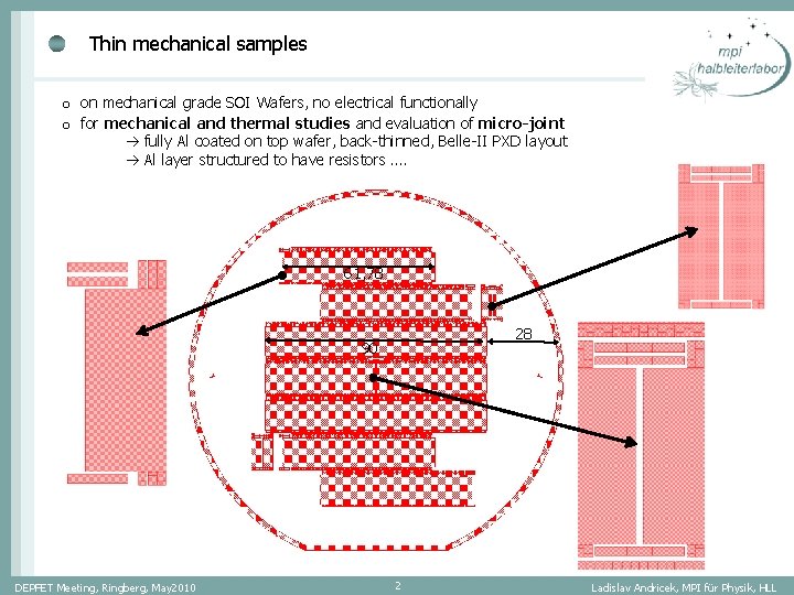
Thin mechanical samples o on mechanical grade SOI Wafers, no electrical functionally o for mechanical and thermal studies and evaluation of micro-joint fully Al coated on top wafer, back-thinned, Belle-II PXD layout Al layer structured to have resistors …. 61, 78 28 90 DEPFET Meeting, Ringberg, May 2010 2 Ladislav Andricek, MPI für Physik, HLL
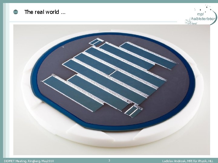
The real world … DEPFET Meeting, Ringberg, May 2010 3 Ladislav Andricek, MPI für Physik, HLL
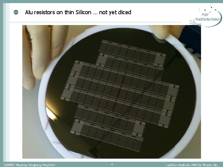
Alu resistors on thin Silicon … not yet diced DEPFET Meeting, Ringberg, May 2010 4 Ladislav Andricek, MPI für Physik, HLL
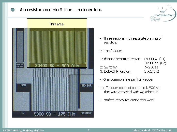
Alu resistors on thin Silicon – a closer look Thin area -: Three regions with separate biasing of resistors Per half-ladder: 1: thinned sensitive region 2: Switcher 3: DCD/DHP Region 6 x 900 Ω (L 1) 8 x 900 Ω (L 2) 6 x 250 Ω 1 x. R 175 Ω -: One common line per half-ladder -: off-ladder connection at thick EOS via thin wire attached with Ag adhesive -: wafers ready for dicing this week DEPFET Meeting, Ringberg, May 2010 5 Ladislav Andricek, MPI für Physik, HLL
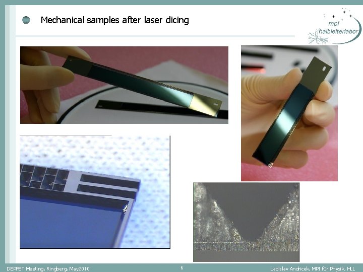
Mechanical samples after laser dicing DEPFET Meeting, Ringberg, May 2010 6 Ladislav Andricek, MPI für Physik, HLL
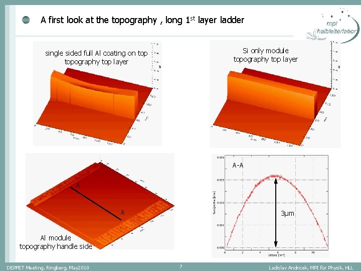
A first look at the topography , long 1 st layer ladder Si only module topography top layer single sided full Al coating on topography top layer A-A A A 3µm Al module topography handle side DEPFET Meeting, Ringberg, May 2010 7 Ladislav Andricek, MPI für Physik, HLL
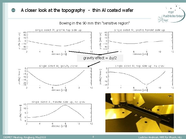
A closer look at the topography - thin Al coated wafer Bowing in the 90 mm thin “sensitive region” gravity effect = Δy/2 DEPFET Meeting, Ringberg, May 2010 8 Ladislav Andricek, MPI für Physik, HLL
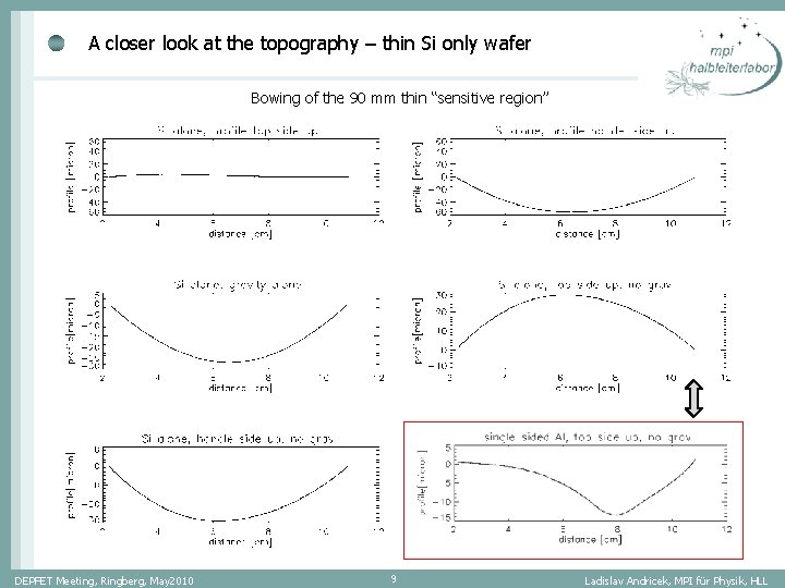
A closer look at the topography – thin Si only wafer Bowing of the 90 mm thin “sensitive region” DEPFET Meeting, Ringberg, May 2010 9 Ladislav Andricek, MPI für Physik, HLL
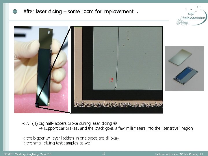
After laser dicing – some room for improvement. . -: All (!!) big half-ladders broke during laser dicing support bar brakes, and the crack goes a few millimeters into the “sensitive” region -: the bigger 1 st layer ladders in one piece are all okay -: the small gluing test samples as well DEPFET Meeting, Ringberg, May 2010 10 Ladislav Andricek, MPI für Physik, HLL
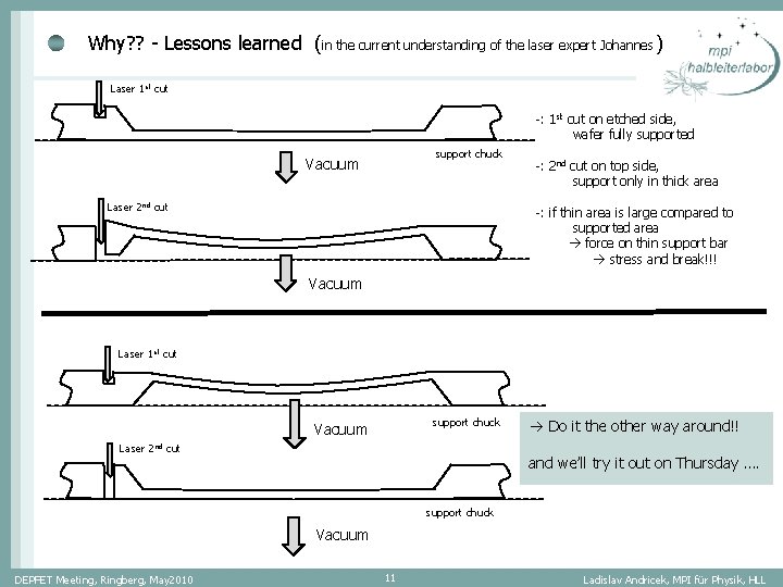
Why? ? - Lessons learned (in the current understanding of the laser expert Johannes ) Laser 1 st cut -: 1 st cut on etched side, wafer fully supported support chuck Vacuum Laser 2 nd cut -: 2 nd cut on top side, support only in thick area -: if thin area is large compared to supported area force on thin support bar stress and break!!! Vacuum Laser 1 st cut support chuck Vacuum Laser 2 nd cut Do it the other way around!! and we’ll try it out on Thursday …. support chuck Vacuum DEPFET Meeting, Ringberg, May 2010 11 Ladislav Andricek, MPI für Physik, HLL
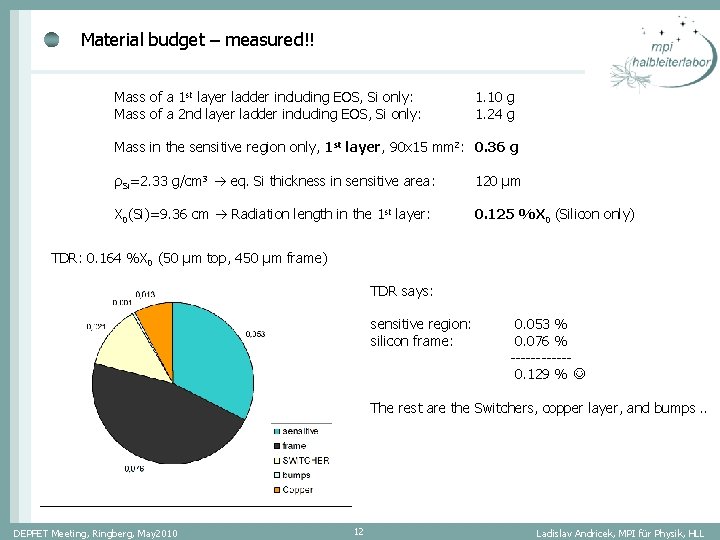
Material budget – measured!! Mass of a 1 st layer ladder including EOS, Si only: Mass of a 2 nd layer ladder including EOS, Si only: 1. 10 g 1. 24 g Mass in the sensitive region only, 1 st layer, 90 x 15 mm 2: 0. 36 g ρSi=2. 33 g/cm 3 eq. Si thickness in sensitive area: 120 µm X 0(Si)=9. 36 cm Radiation length in the 1 st layer: 0. 125 %X 0 (Silicon only) TDR: 0. 164 %X 0 (50 µm top, 450 µm frame) TDR says: sensitive region: silicon frame: 0. 053 % 0. 076 % ------0. 129 % The rest are the Switchers, copper layer, and bumps. . DEPFET Meeting, Ringberg, May 2010 12 Ladislav Andricek, MPI für Physik, HLL
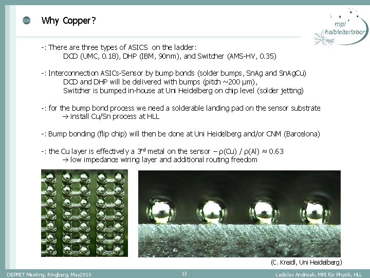
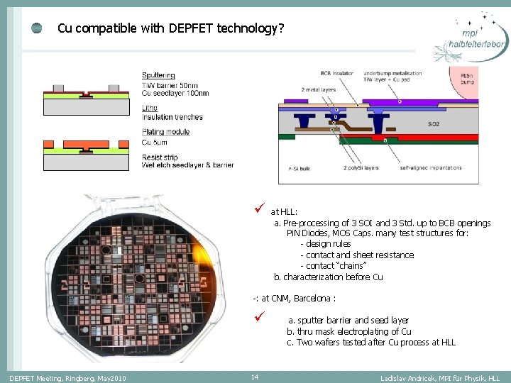
Why Copper? -: There are three types of ASICS on the ladder: DCD (UMC, 0. 18), DHP (IBM, 90 nm), and Switcher (AMS-HV, 0. 35) -: Interconnection ASICs-Sensor by bump bonds (solder bumps, Sn. Ag and Sn. Ag. Cu) DCD and DHP will be delivered with bumps (pitch ~200 µm), Switcher is bumped in-house at Uni Heidelberg on chip level (solder jetting) -: for the bump bond process we need a solderable landing pad on the sensor substrate install Cu/Sn process at HLL -: Bump bonding (flip chip) will then be done at Uni Heidelberg and/or CNM (Barcelona) -: the Cu layer is effectively a 3 rd metal on the sensor – ρ(Cu) / ρ(Al) ≈ 0. 63 low impedance wiring layer and additional routing freedom (C. Kreidl, Uni Heidelberg) DEPFET Meeting, Ringberg, May 2010 13 Ladislav Andricek, MPI für Physik, HLL
Cu compatible with DEPFET technology? ü at HLL: a. Pre-processing of 3 SOI and 3 Std. up to BCB openings Pi. N Diodes, MOS Caps. many test structures for: - design rules - contact and sheet resistance - contact “chains” b. characterization before Cu -: at CNM, Barcelona : ü DEPFET Meeting, Ringberg, May 2010 14 a. sputter barrier and seed layer b. thru mask electroplating of Cu c. Two wafers tested after Cu process at HLL Ladislav Andricek, MPI für Physik, HLL
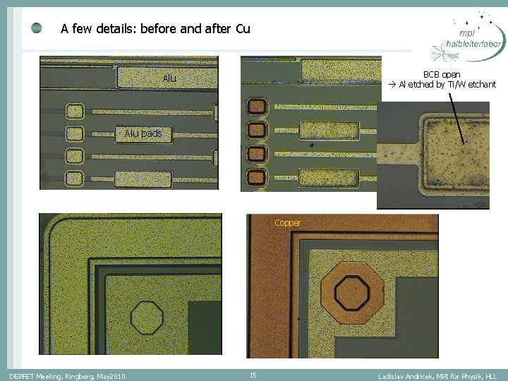
A few details: before and after Cu BCB open Al etched by Ti/W etchant Alu pads Copper DEPFET Meeting, Ringberg, May 2010 15 Ladislav Andricek, MPI für Physik, HLL
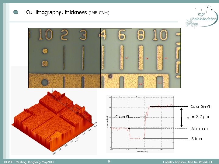
Cu lithography, thickness (IMB-CNM) Cu on Si+Al Cu on Si t. Cu = 2. 2 µm Aluminum Silicon DEPFET Meeting, Ringberg, May 2010 16 Ladislav Andricek, MPI für Physik, HLL
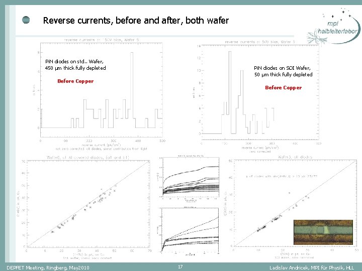
Reverse currents, before and after, both wafer Pi. N diodes on std. . Wafer, 450 µm thick fully depleted Pi. N diodes on SOI Wafer, 50 µm thick fully depleted Before Copper DEPFET Meeting, Ringberg, May 2010 17 Ladislav Andricek, MPI für Physik, HLL
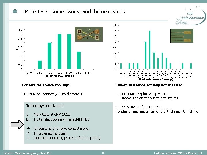
More tests, some issues, and the next steps 8 4. 5 7 4 6 3. 5 2. 5 4 # 5 # 3 2 3 1. 5 2 1 1 0 0 3, 00 3, 50 4, 00 4, 50 5, 00 contact resistance (Ohm) 5, 50 8, 00 8, 50 9, 00 9, 50 10, 00 10, 50 11, 00 11, 50 12, 00 12, 50 13, 00 13, 50 14, 00 14, 50 15, 00 15, 50 16, 00 More 0. 5 More Sheet resistance (m. Ohm/sqr) Contact resistance too high: Sheet resistance actually not that bad: 4. 4 Ω per contact (20 µm diameter) 11. 8 mΩ/sq for 2. 2 µm Cu (measured on various test structures) Technology optimization: a. b. New tests at CNM 2010 Install electroplating line at MPI HLL Understand solve contact issue Improve etch process Optimize annealing process after Cu plating DEPFET Meeting, Ringberg, May 2010 Bulk resistivity of Cu 1. 7µΩcm ideal sheet resistance for this thickness: 8 mΩ/sq 18 Ladislav Andricek, MPI für Physik, HLL
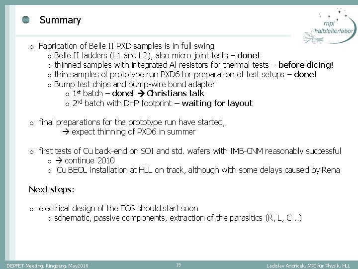
Summary o Fabrication of Belle II PXD samples is in full swing o Belle II ladders (L 1 and L 2), also micro joint tests – done! o thinned samples with integrated Al-resistors for thermal tests – before dicing! o thin samples of prototype run PXD 6 for preparation of test setups – done! o Bump test chips and bump-wire bond adapter o 1 st batch – done! Christians talk o 2 nd batch with DHP footprint – waiting for layout o final preparations for the prototype run have started, expect thinning of PXD 6 in summer o first tests of Cu back-end on SOI and std. wafers with IMB-CNM reasonably successful o continue 2010 o Cu BEOL installation at HLL on track, although with some delays caused by Rena Next steps: o electrical design of the EOS should start soon o schematic, passive components, extraction of the parasitics (R, L, C. . ) DEPFET Meeting, Ringberg, May 2010 19 Ladislav Andricek, MPI für Physik, HLL
Backup slides follow DEPFET Meeting, Ringberg, May 2010 20 Ladislav Andricek, MPI für Physik, HLL
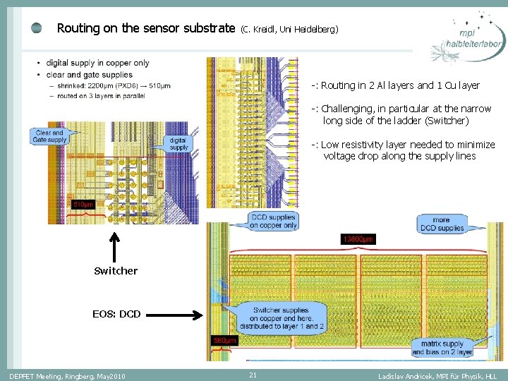
Routing on the sensor substrate (C. Kreidl, Uni Heidelberg) -: Routing in 2 Al layers and 1 Cu layer -: Challenging, in particular at the narrow long side of the ladder (Switcher) -: Low resistivity layer needed to minimize voltage drop along the supply lines Switcher EOS: DCD DEPFET Meeting, Ringberg, May 2010 21 Ladislav Andricek, MPI für Physik, HLL
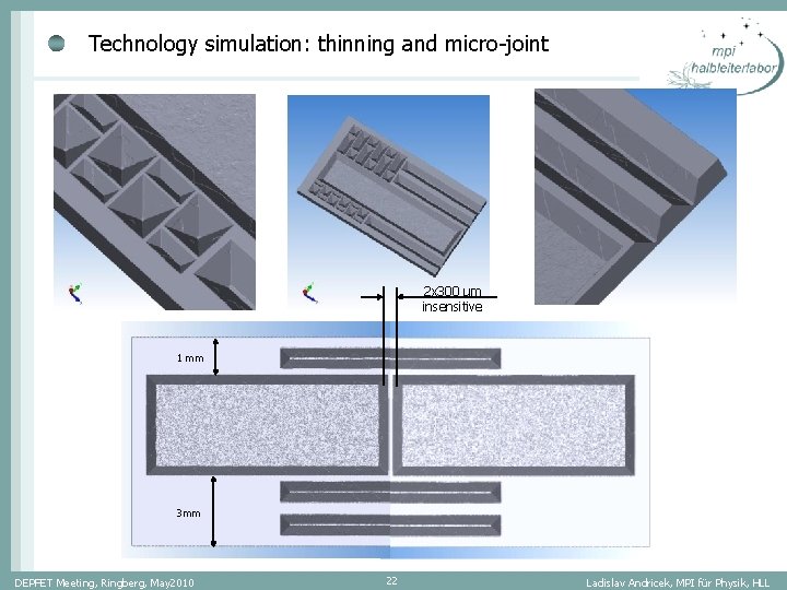
Technology simulation: thinning and micro-joint 2 x 300 µm insensitive 1 mm 3 mm DEPFET Meeting, Ringberg, May 2010 22 Ladislav Andricek, MPI für Physik, HLL
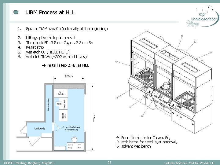
UBM Process at HLL 1. Sputter Ti: W und Cu (externally at the beginning) 2. 3. 4. 5. 6. Lithography: thick photo resist Thru mask EP: 3 -5 um Cu, ca. 2 -3 um Sn Resist strip wet etch Cu (Fe. Cl 3, HCl. . ) wet etch Ti: W: (H 2 O 2 with additives) install step 2. -6. at HLL Fountain plater for Cu and Sn, etch baths for seed layer removal, solvent wet bench DEPFET Meeting, Ringberg, May 2010 23 Ladislav Andricek, MPI für Physik, HLL