Nanoscience Nanotechnology and Nanomanufacturing Exciting new science and

- Slides: 24

Nanoscience, Nanotechnology and Nanomanufacturing Exciting new science and technology for the 21 st century

Nanotechnology • Is a broad, interdisciplinary topic involving physics, chemistry, biology and engineering • It has potential impact in electronics, health, energy, materials, and a wide variety of other application areas.

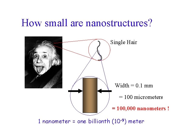
How small are nanostructures? Single Hair Width = 0. 1 mm = 100 micrometers = 100, 000 nanometers ! 1 nanometer = one billionth (10 -9) meter

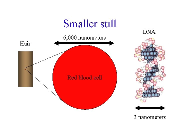
Smaller still Hair 6, 000 nanometers DNA . Red blood cell 3 nanometers

How do we make nanostructures? How do we see nanostructures?

First, how do we make nanostructures? • Lithography • Self-assembly - physical or chemical

Lithography Mark Tuominen

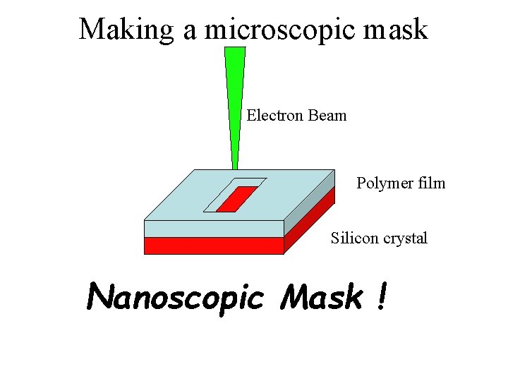
Making a microscopic mask Electron Beam Polymer film Silicon crystal Nanoscopic Mask !

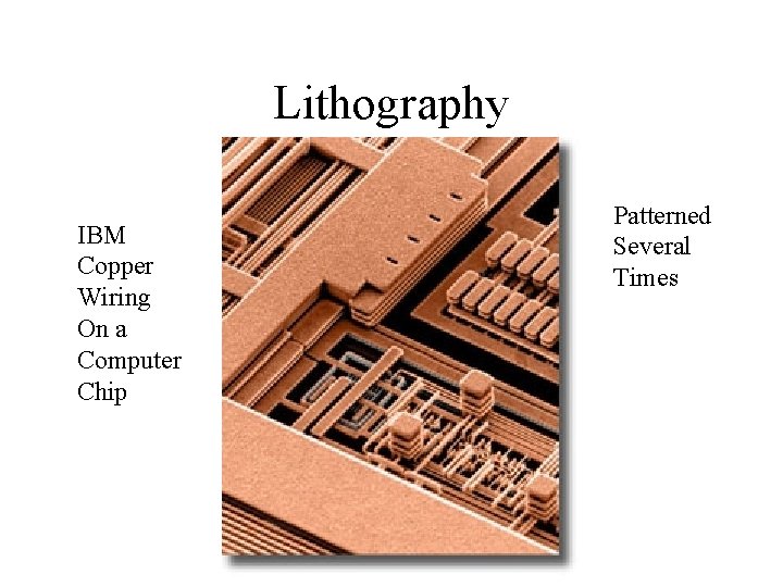
Lithography IBM Copper Wiring On a Computer Chip Patterned Several Times

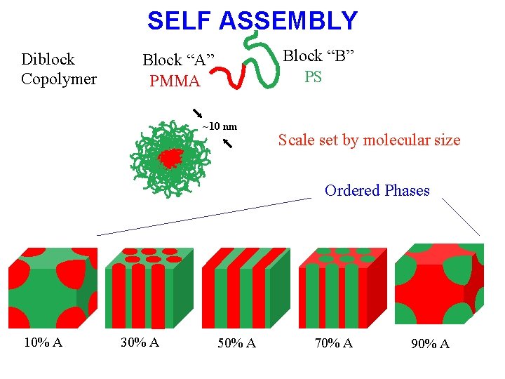
SELF ASSEMBLY Diblock Copolymer Block “B” PS Block “A” PMMA ~10 nm Scale set by molecular size Ordered Phases 10% A 30% A 50% A 70% A 90% A

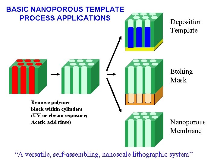
BASIC NANOPOROUS TEMPLATE PROCESS APPLICATIONS Deposition Template Etching Mask Remove polymer block within cylinders (UV or ebeam exposure; Acetic acid rinse) Nanoporous Membrane “A versatile, self-assembling, nanoscale lithographic system”

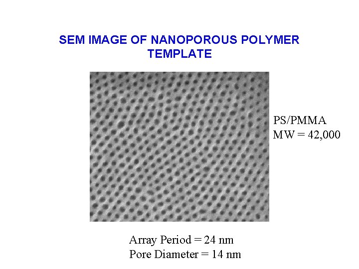
SEM IMAGE OF NANOPOROUS POLYMER TEMPLATE PS/PMMA MW = 42, 000 Array Period = 24 nm Pore Diameter = 14 nm

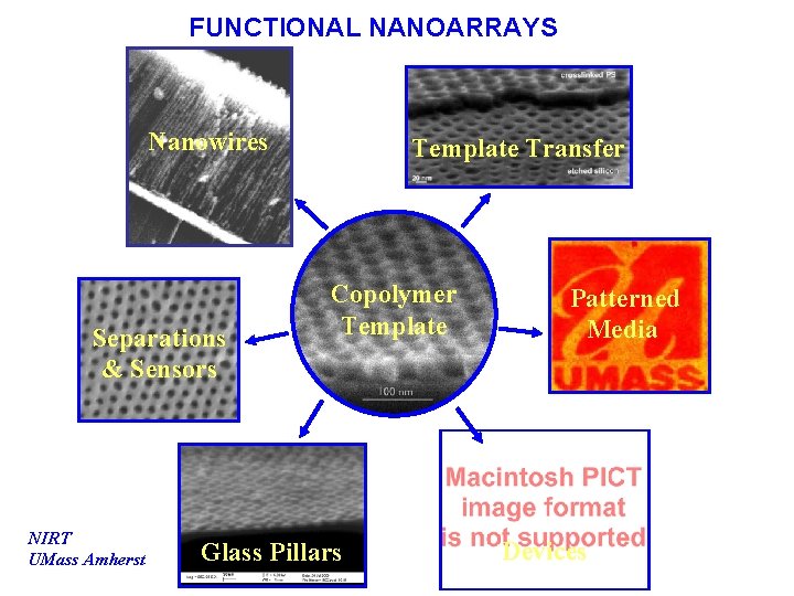
FUNCTIONAL NANOARRAYS Nanowires Separations & Sensors NIRT UMass Amherst Template Transfer Copolymer Template Glass Pillars Patterned Media Devices

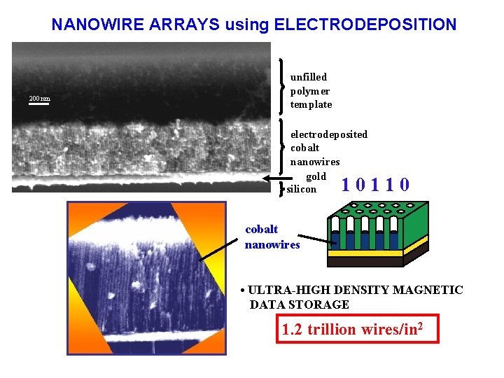
NANOWIRE ARRAYS using ELECTRODEPOSITION unfilled polymer template 200 nm electrodeposited cobalt nanowires gold silicon 10110 100 nm 20 nm cobalt nanowires • ULTRA-HIGH DENSITY MAGNETIC DATA STORAGE 1. 2 trillion wires/in 2

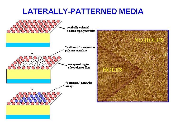
LATERALLY-PATTERNED MEDIA vertically-oriented diblock copolymer film NO HOLES “patterned” nanoporous polymer template unexposed region of copolymer film “patterned” nanowire array HOLES

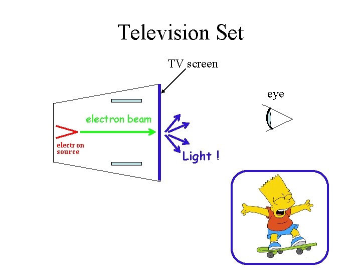
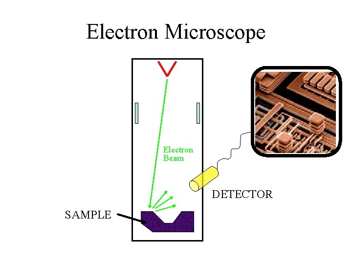
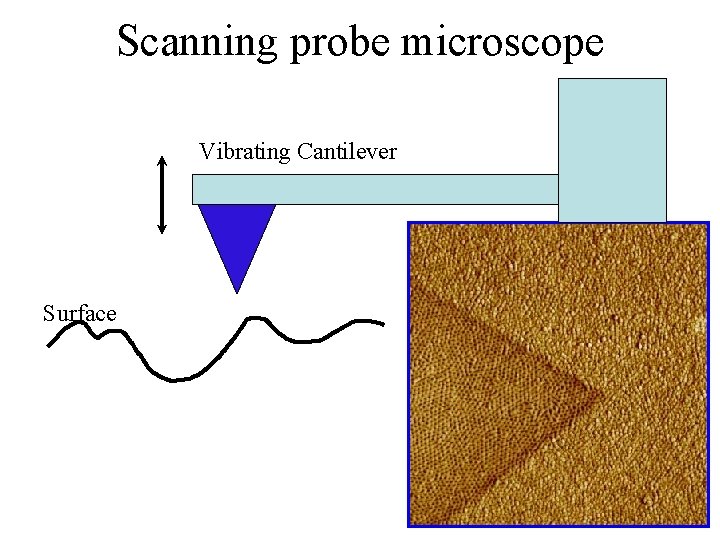
How do we see nanostructures? • A light microscope? • An electron microscope! • A scanning probe microscope!

Television Set TV screen eye electron beam electron source Light !

Electron Microscope Electron Beam DETECTOR SAMPLE

Scanning probe microscope Vibrating Cantilever Surface

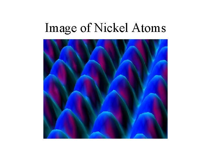
Image of Nickel Atoms

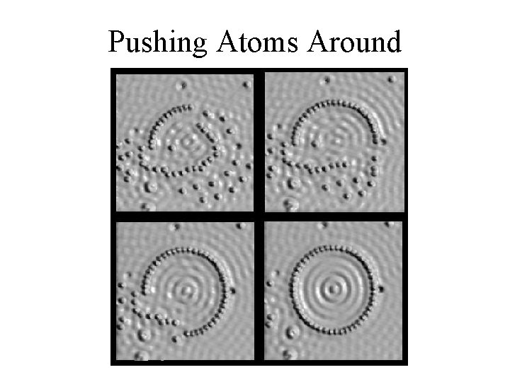
Pushing Atoms Around

The New UMass Nano Center Hierarchical?

Hierarchical Structures Example: google maps Earth -- countries -- states -- cities -- blocks -- houses -- rooms

Hierarchical Structures Examples in Nano: Biological Cell and Computer Chip In nanomanufacturing we are integrating "bottom up" self-assembly with "top down" lithography —Hierarchical Manufacturing!