
Lecture 10 Chemical Engineering for MicroNano Fabrication Minoan
Lecture 10 Chemical Engineering for Micro/Nano Fabrication Minoan Signet Ring From the Bronze Age Ch. E 384 T / 323
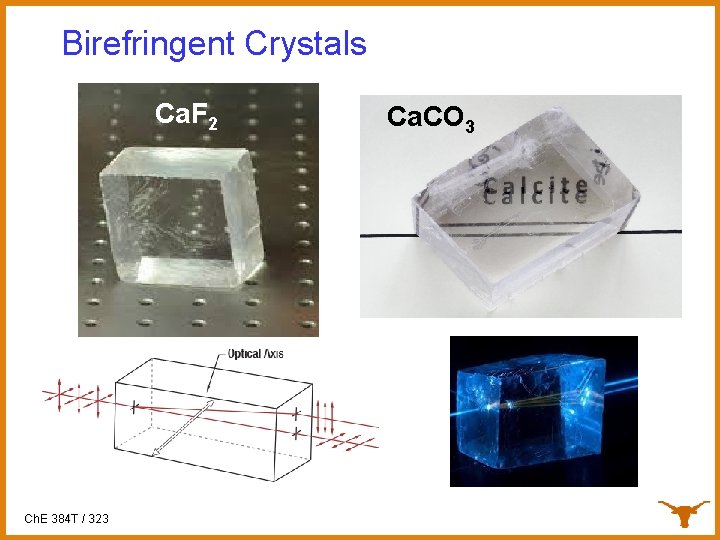
Birefringent Crystals Ca. F 2 Ch. E 384 T / 323 Ca. CO 3

Frogs Ch. E 384 T / 323

Pattern Density Effects Easiest… Easy… Very Difficult! “Residual layer” Ch. E 384 T / 323

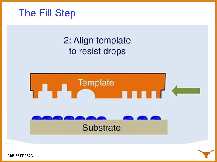
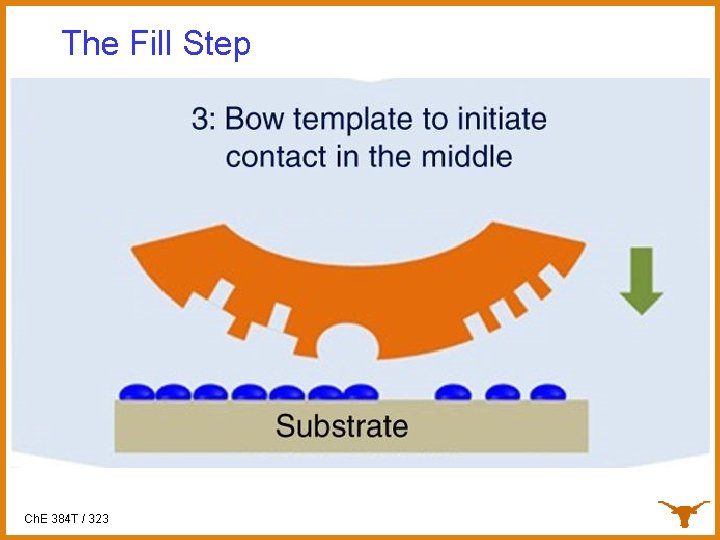
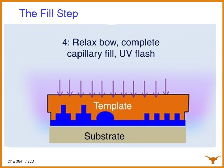
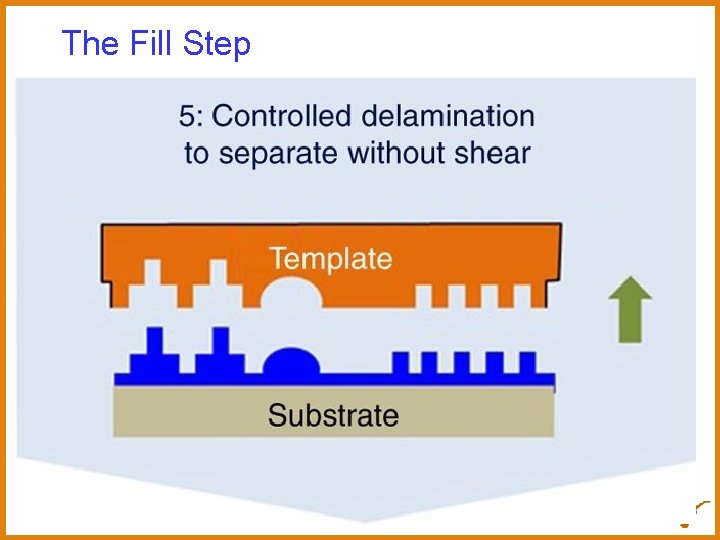
Step and Flash Imprint Lithography Fused silica template, coated with release layer Template Step 1: Dispense drops Step 2: Lower template and fill pattern Step 3: Polymerize S-FIL fluid with UV exposure Step 4: Separate template from substrate Ch. E 384 T / 323 • S-FIL fluid dispenser Planarization layer Substrate Template Planarization layer Substrate • Ink jet system • Template filling driven by capillary action • low imprint pressure and room temperature process Template Planarization layer Substrate Step & Repeat

S-FIL vs. Optical Lithography Schematic Greatly simplified and lower cost process Imprint Lithography Ch. E 384 T / 323 Standard Optical Lithography
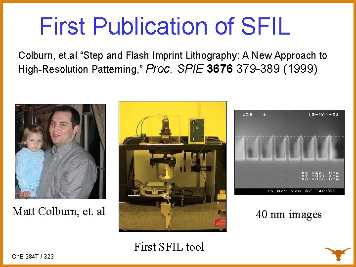
First Publication of SFIL Colburn, et. al “Step and Flash Imprint Lithography: A New Approach to High-Resolution Patterning, ” Proc. SPIE 3676 379 -389 (1999) Matt Colburn, et. al 40 nm images First SFIL tool Ch. E 384 T / 323
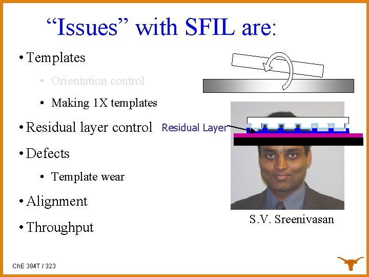
“Issues” with SFIL are: • Templates • Orientation control • Making 1 X templates • Residual layer control Residual Layer • Defects • Template wear • Alignment • Throughput Ch. E 384 T / 323 S. V. Sreenivasan
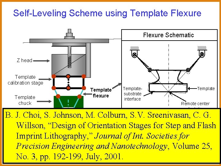
Self-Leveling Scheme using Template Flexure Schematic Z head Template calibration stage Template chuck Template flexure Templatesubstrate interface Template Remote center of rotation B. Template J. Choi, S. Johnson, M. Colburn, S. V. Sreenivasan, C. G. Wafer Willson, “Design of Orientation Stages for Step and Flash stage Imprint Lithography, ” Journal of. Wafer Int. Tip/Tilt Societies for Theta stage Precision Engineering and Nanotechnology, Volume 25, XY stage No. / 3233, pp. 192 -199, July, 2001. Ch. E 384 T
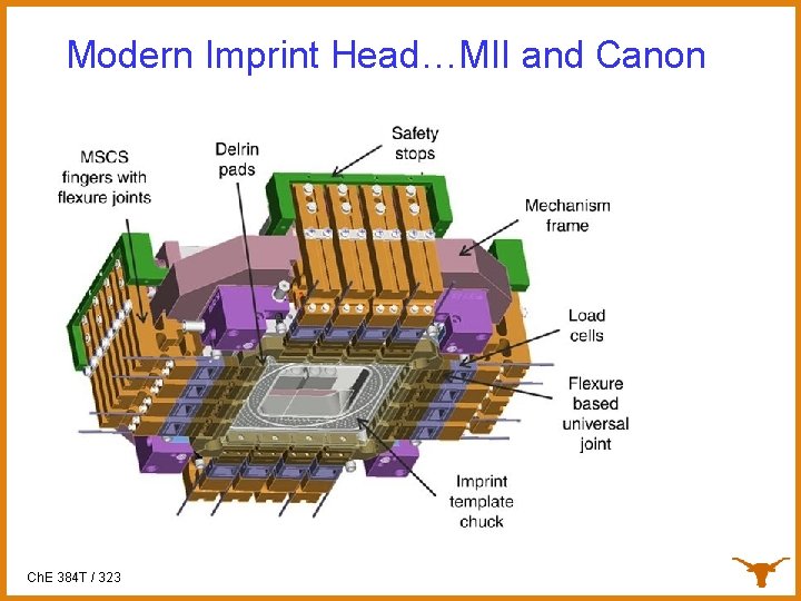
Modern Imprint Head…MII and Canon Ch. E 384 T / 323
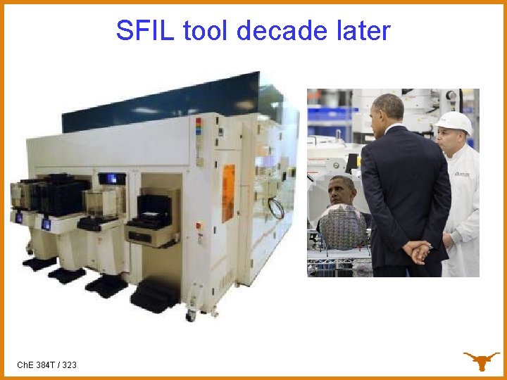
SFIL tool decade later Ch. E 384 T / 323
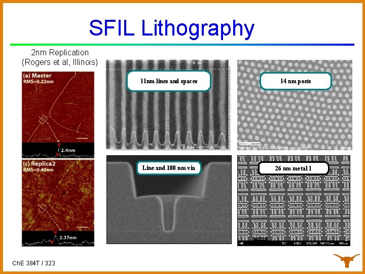
SFIL Lithography 2 nm Replication (Rogers et al, Illinois) 11 nm lines and spaces Line and 100 nm via Ch. E 384 T / 323 14 nm posts 26 nm metal 1
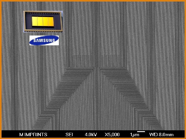
Gate Level: 38 nm Half Pitch Ch. E 384 T / 323
Ch. E 384 T / 323
Claims of competitors and detractors Obviously, you cannot ……. 4 control residual layer thickness 4 manage defects…. no pellicle? ? ? 4 achieve layer to layer alignment 4 achieve workable throughput 4 Abut fields, etc. Ch. E 384 T / 323
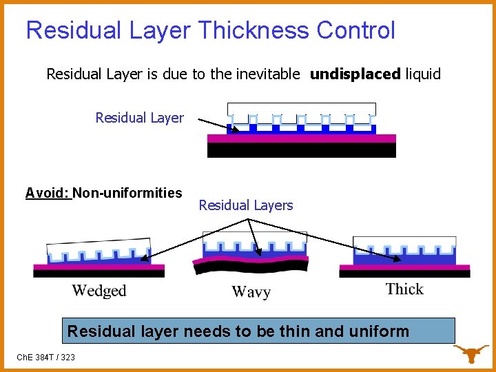
Residual Layer Thickness Control Residual Layer is due to the inevitable undisplaced liquid Residual Layer Avoid: Non-uniformities Residual Layers Residual layer needs to be thin and uniform Ch. E 384 T / 323
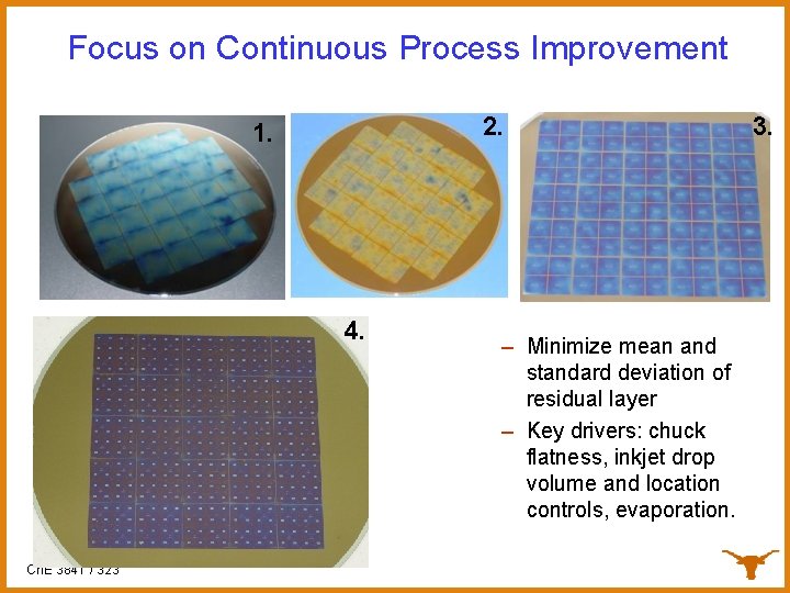
Focus on Continuous Process Improvement 2. 1. 4. Ch. E 384 T / 323 – Minimize mean and standard deviation of residual layer – Key drivers: chuck flatness, inkjet drop volume and location controls, evaporation. 3.
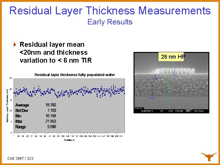
Residual Layer Thickness Measurements Early Results 4 Residual layer mean <20 nm and thickness variation to < 6 nm TIR Residual layer thickness fully populated wafer Ch. E 384 T / 323 28 nm HP
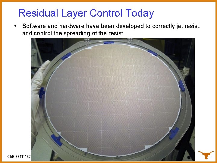
Residual Layer Control Today • Software and hardware have been developed to correctly jet resist, and control the spreading of the resist. Ch. E 384 T / 323

Defects 1) Why do you think 1 X projection lithography replaced contact printing in the early 80’s? ? Don’t you learn from history? ? 2) Do you propose attempt to do lithography without a pellicle? ? !! Ch. E 384 T / 323
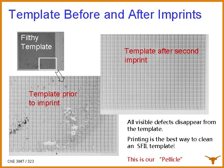
Template Before and After Imprints Filthy Template after second imprint Template prior to imprint All visible defects disappear from the template. Printing is the best way to clean an SFIL template! Ch. E 384 T / 323 This is our “Pellicle”
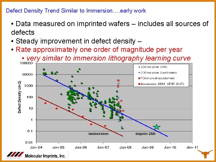
Defect Density Trend Similar to Immersion…. early work • Data measured on imprinted wafers – includes all sources of defects • Steady improvement in defect density – • Rate approximately one order of magnitude per year • very similar to immersion lithography learning curve Ch. E 384 T / 323
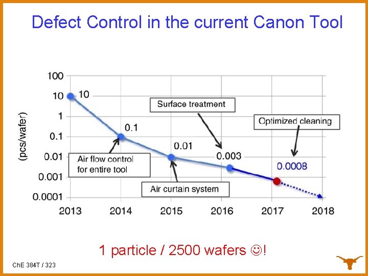
Defect Control in the current Canon Tool 1 particle / 2500 wafers ! Ch. E 384 T / 323
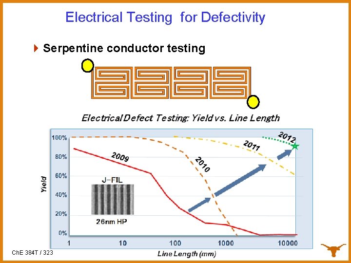
Electrical Testing for Defectivity 4 Serpentine conductor testing Ch. E 384 T / 323
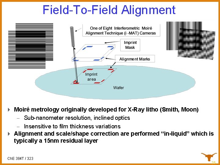
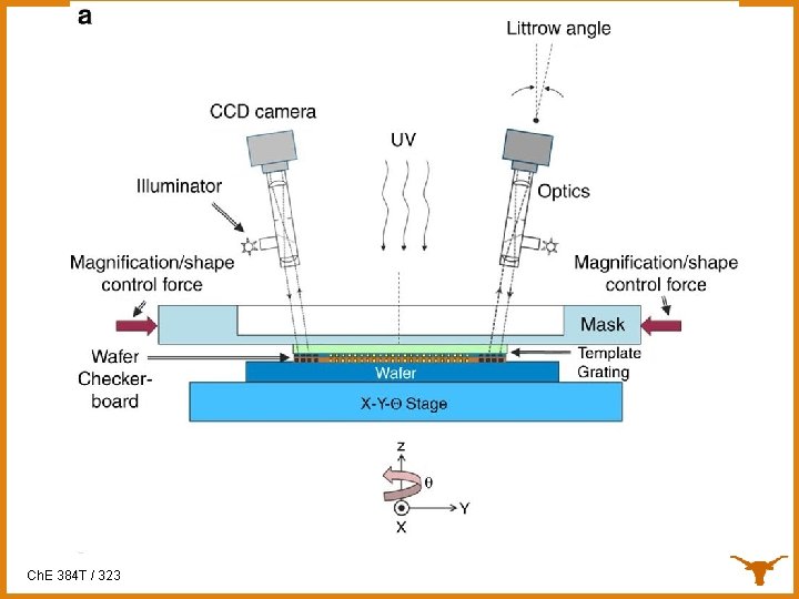
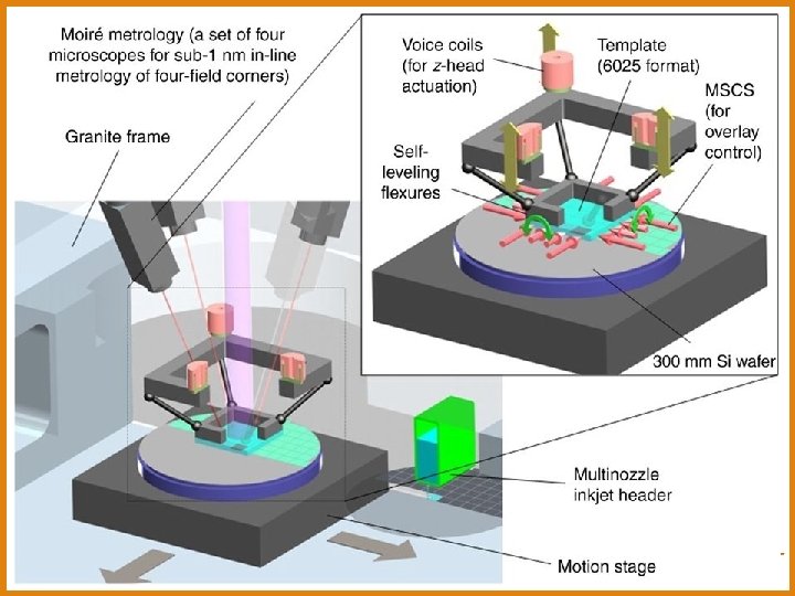
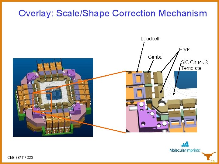
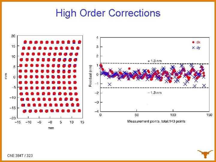
Field-To-Field Alignment 4 Moiré metrology originally developed for X-Ray litho (Smith, Moon) - Sub-nanometer resolution, inclined optics - Insensitive to film thickness variations 4 Alignment and scale/shape correction are performed “in-liquid” which is typically a 15 nm residual layer Ch. E 384 T / 323 25
Ch. E 384 T / 323
Ch. E 384 T / 323
Overlay: Scale/Shape Correction Mechanism Loadcell Pads Gimbal Si. C Chuck & Template Ch. E 384 T / 323 28
High Order Corrections Ch. E 384 T / 323
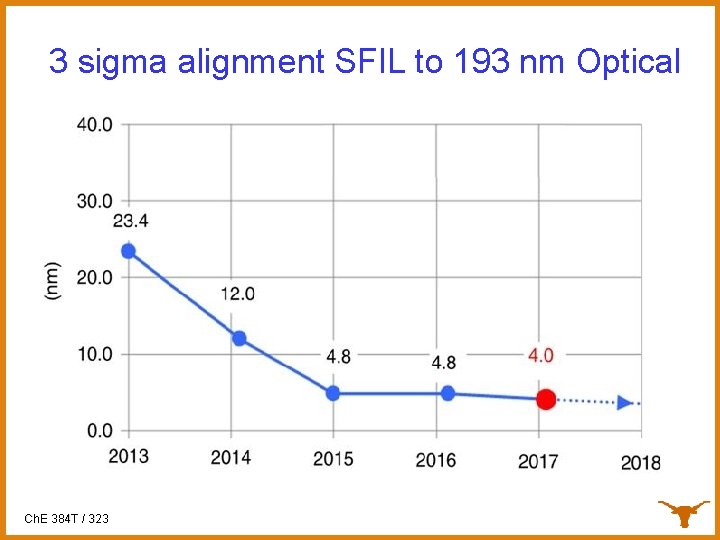
3 sigma alignment SFIL to 193 nm Optical Ch. E 384 T / 323
Ch. E 384 T / 323
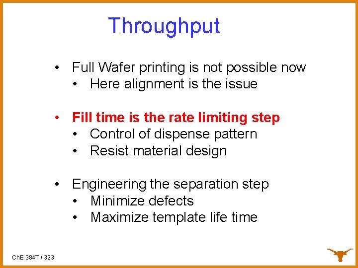
Throughput • Full Wafer printing is not possible now • Here alignment is the issue • Fill time is the rate limiting step • Control of dispense pattern • Resist material design • Engineering the separation step • Minimize defects • Maximize template life time Ch. E 384 T / 323
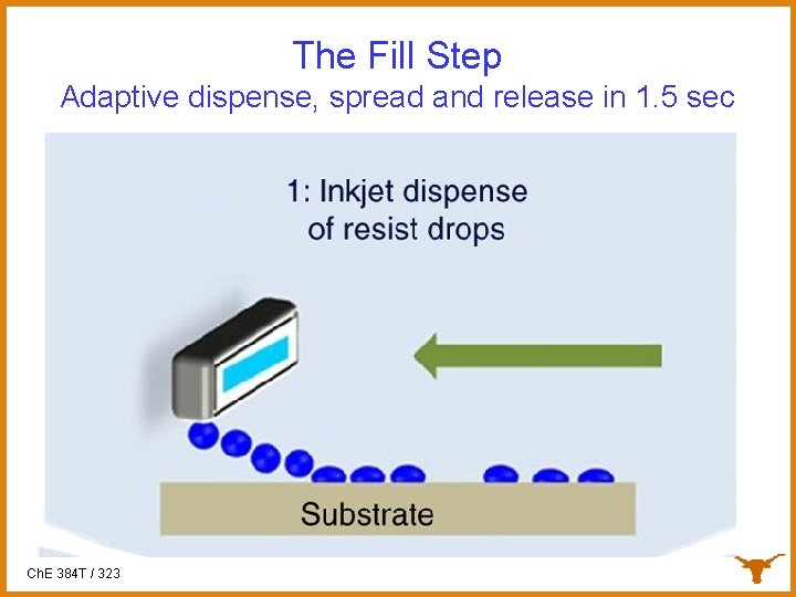
The Fill Step Adaptive dispense, spread and release in 1. 5 sec Ch. E 384 T / 323
The Fill Step Ch. E 384 T / 323
The Fill Step Ch. E 384 T / 323
The Fill Step Ch. E 384 T / 323
The Fill Step Ch. E 384 T / 323
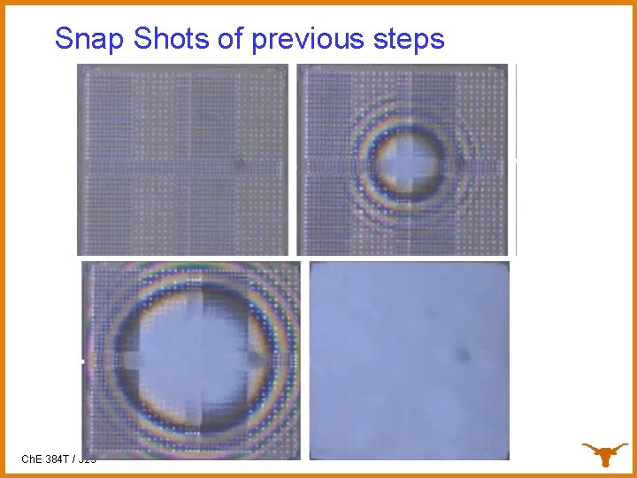
Snap Shots of previous steps Ch. E 384 T / 323
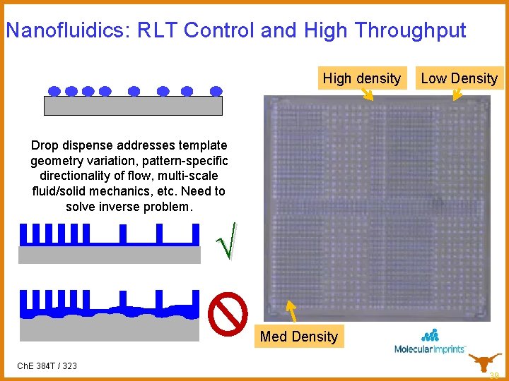
Nanofluidics: RLT Control and High Throughput High density Low Density Drop dispense addresses template geometry variation, pattern-specific directionality of flow, multi-scale fluid/solid mechanics, etc. Need to solve inverse problem. √ Med Density Ch. E 384 T / 323 39
- Slides: 39