Chapter 4 Diodes Diode Simple nonlinear device 2
- Slides: 40

Chapter 4. Diodes

Diode • Simple non-linear device • 2 terminal device, uni- or bi-directional current flow • Semiconductor • Many types – pn-junction diode – Photo diode – Light emitting diode – Zener diode Copyright 2004 by Oxford University Press, Inc.

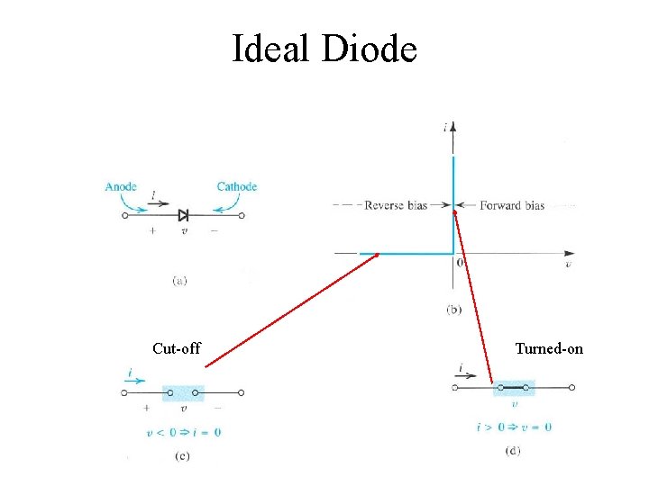
Ideal Diode Cut-off Turned-on Copyright 2004 by Oxford University Press, Inc.

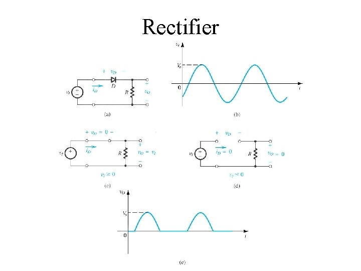
Rectifier Copyright 2004 by Oxford University Press, Inc.

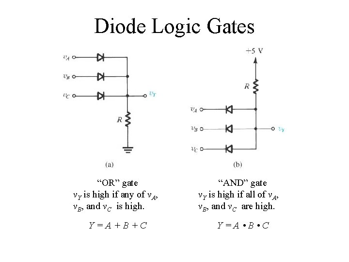
Diode Logic Gates “OR” gate v. Y is high if any of v. A, v. B, and v. C is high. Y=A+B+C “AND” gate v. Y is high if all of v. A, v. B, and v. C are high. Y=A • B • C Copyright 2004 by Oxford University Press, Inc.

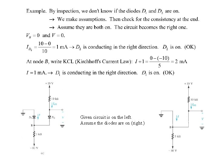
Given circuit is on the left. Assume the diodes are on (right. ) Copyright 2004 by Oxford University Press, Inc.

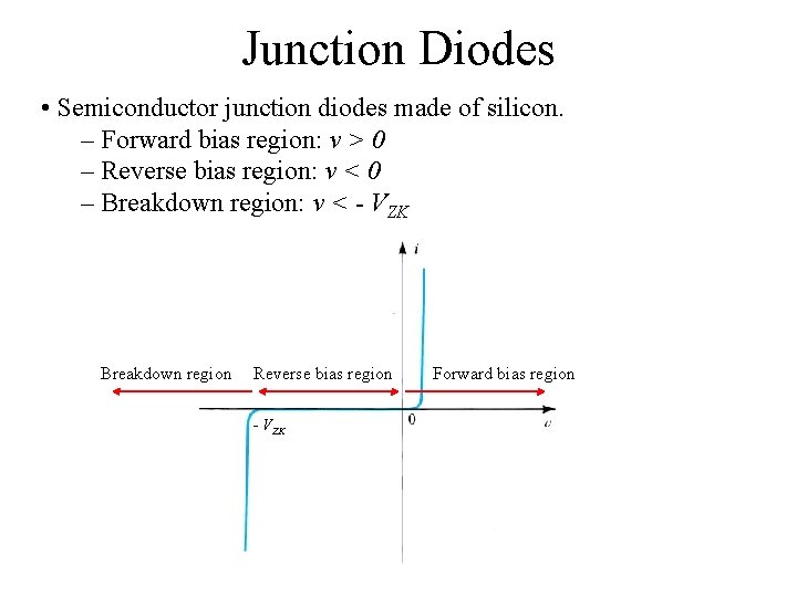
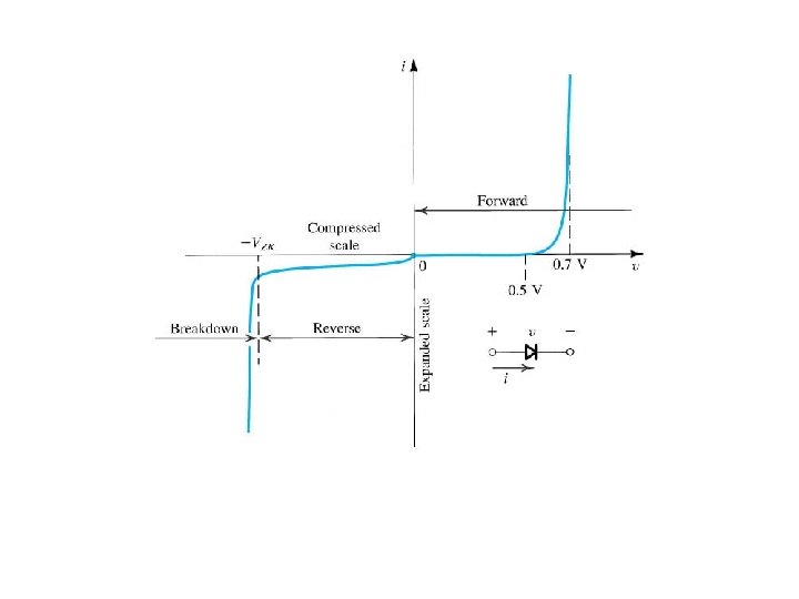
Junction Diodes • Semiconductor junction diodes made of silicon. – Forward bias region: v > 0 – Reverse bias region: v < 0 – Breakdown region: v < - VZK Breakdown region Reverse bias region Forward bias region - VZK Copyright 2004 by Oxford University Press, Inc.

Copyright 2004 by Oxford University Press, Inc.

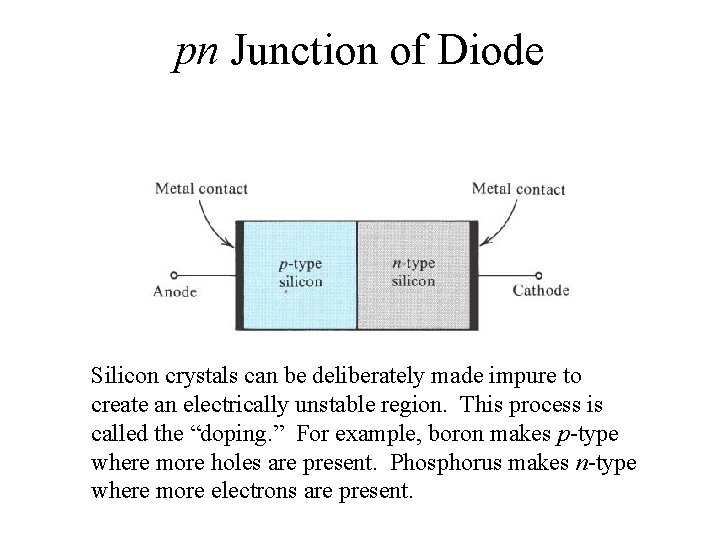
pn Junction of Diode Silicon crystals can be deliberately made impure to create an electrically unstable region. This process is called the “doping. ” For example, boron makes p-type where more holes are present. Phosphorus makes n-type where more electrons are present. Copyright 2004 by Oxford University Press, Inc.

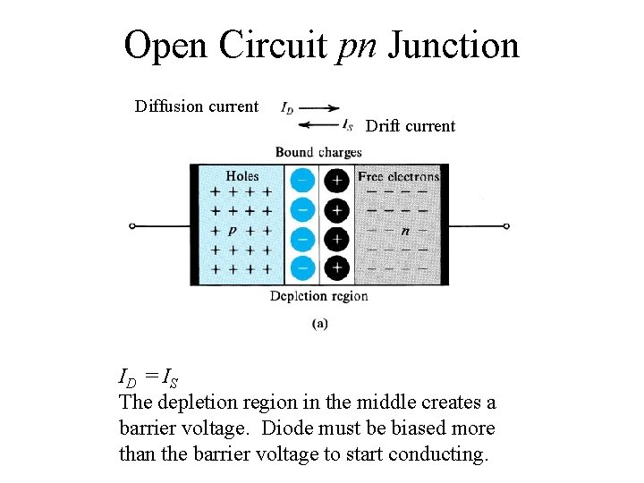
Open Circuit pn Junction Diffusion current Drift current ID = IS The depletion region in the middle creates a barrier voltage. Diode must be biased more than the barrier voltage Copyright to 2004 start by Oxfordconducting. University Press, Inc.

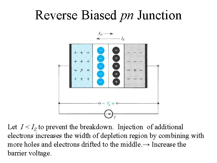
Reverse Biased pn Junction Let I < IS to prevent the breakdown. Injection of additional electrons increases the width of depletion region by combining with more holes and electrons drifted to the middle. → Increase the barrier voltage. Copyright 2004 by Oxford University Press, Inc.

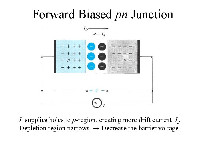
Forward Biased pn Junction I supplies holes to p-region, creating more drift current IS. Depletion region narrows. → Decrease the barrier voltage. Copyright 2004 by Oxford University Press, Inc.

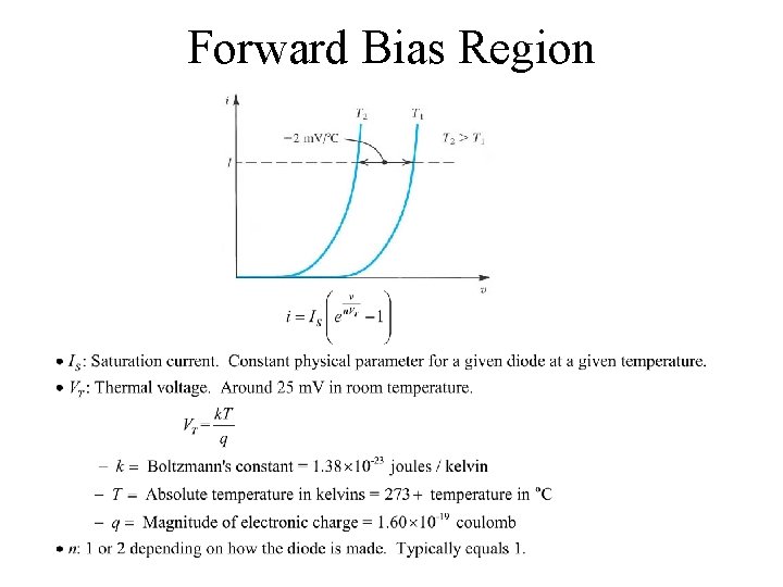
Forward Bias Region Copyright 2004 by Oxford University Press, Inc.

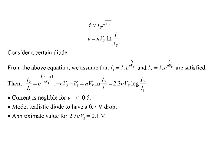
Copyright 2004 by Oxford University Press, Inc.

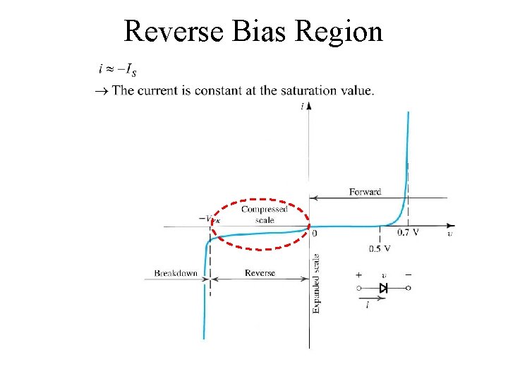
Reverse Bias Region Copyright 2004 by Oxford University Press, Inc.

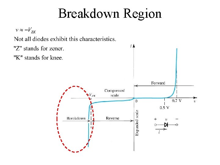
Breakdown Region Copyright 2004 by Oxford University Press, Inc.

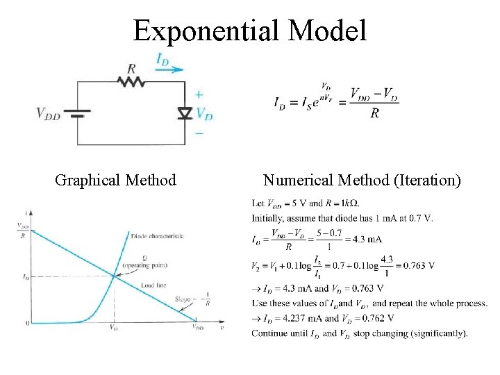
Exponential Model Graphical Method Numerical Method (Iteration) Copyright 2004 by Oxford University Press, Inc.

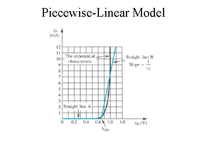
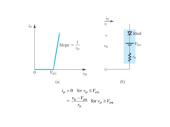
Piecewise-Linear Model Copyright 2004 by Oxford University Press, Inc.

Copyright 2004 by Oxford University Press, Inc.

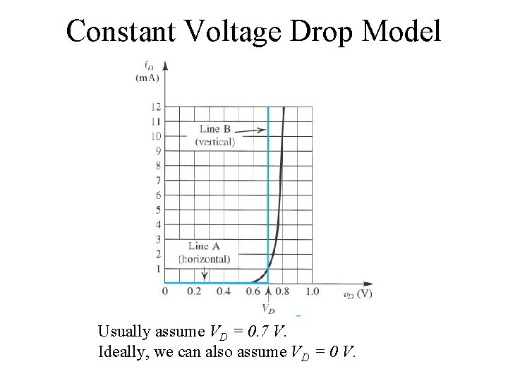
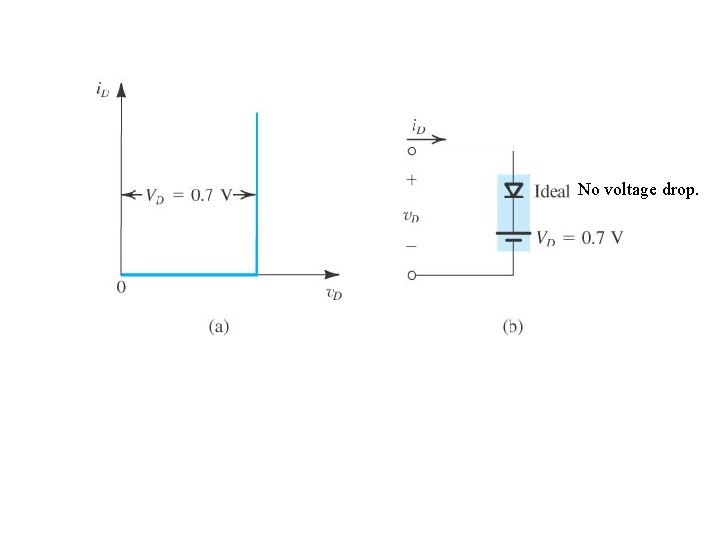
Constant Voltage Drop Model Usually assume VD = 0. 7 V. Ideally, we can also assume VD = 0 V. Copyright 2004 by Oxford University Press, Inc.

No voltage drop. Copyright 2004 by Oxford University Press, Inc.

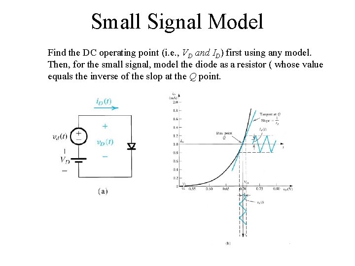
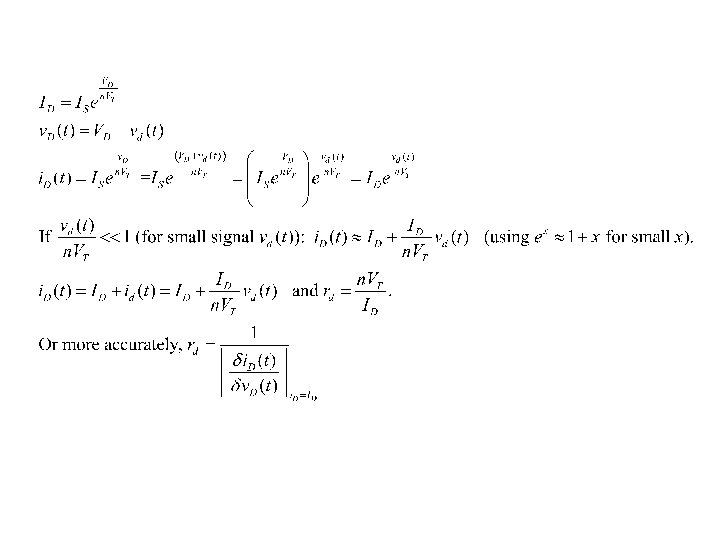
Small Signal Model Find the DC operating point (i. e. , VD and ID) first using any model. Then, for the small signal, model the diode as a resistor ( whose value equals the inverse of the slop at the Q point. Copyright 2004 by Oxford University Press, Inc.

Copyright 2004 by Oxford University Press, Inc.

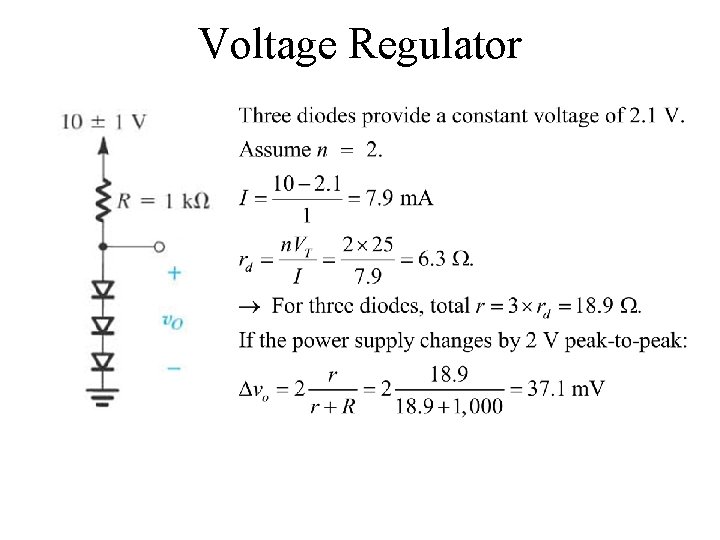
Voltage Regulator Copyright 2004 by Oxford University Press, Inc.

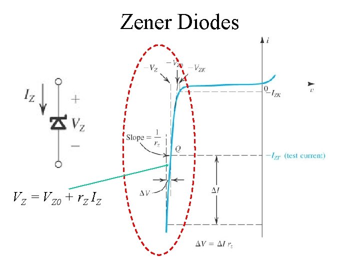
Zener Diodes VZ = VZ 0 + r. Z IZ Copyright 2004 by Oxford University Press, Inc.

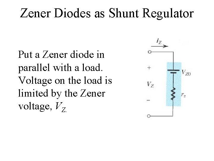
Zener Diodes as Shunt Regulator Put a Zener diode in parallel with a load. Voltage on the load is limited by the Zener voltage, VZ. Copyright 2004 by Oxford University Press, Inc.

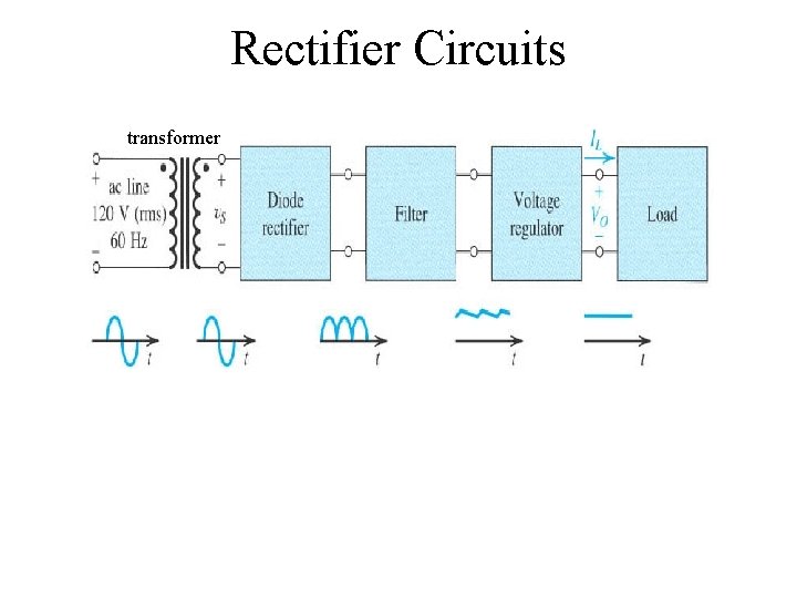
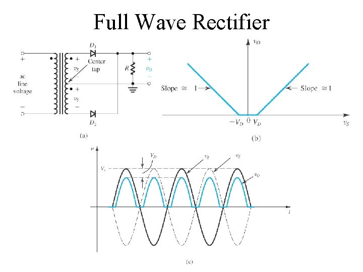
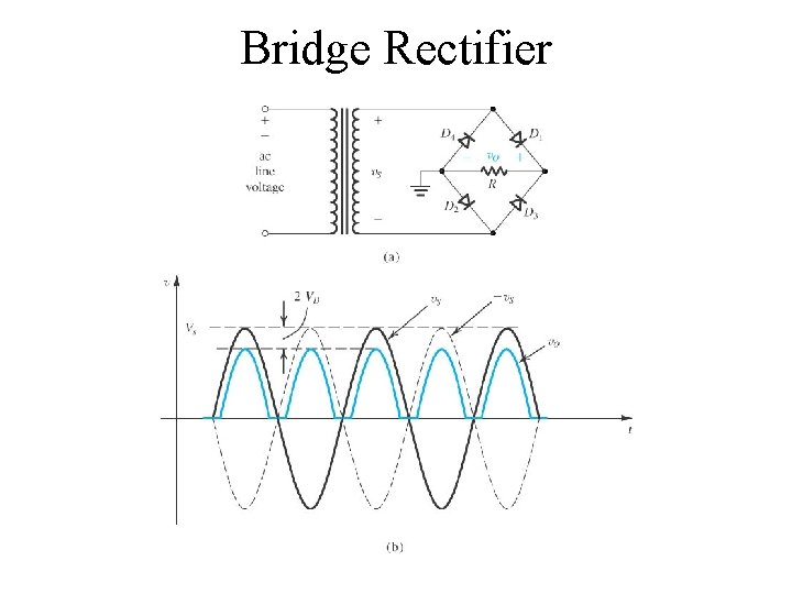
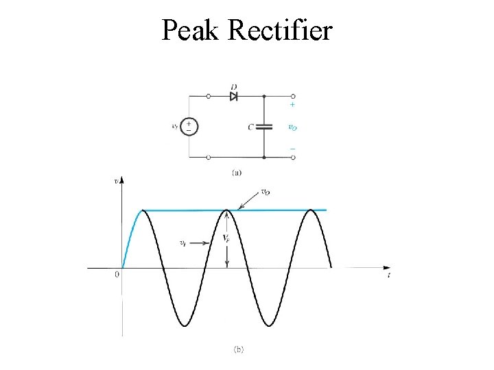
Rectifier Circuits transformer Copyright 2004 by Oxford University Press, Inc.

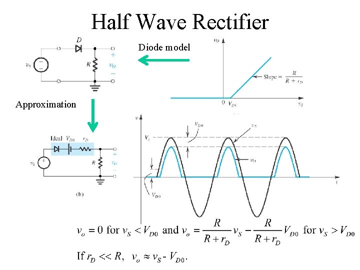
Half Wave Rectifier Diode model Approximation Copyright 2004 by Oxford University Press, Inc.

Full Wave Rectifier Copyright 2004 by Oxford University Press, Inc.

Bridge Rectifier Copyright 2004 by Oxford University Press, Inc.

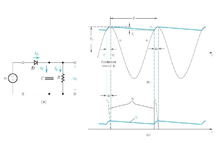
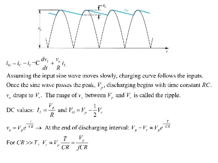
Peak Rectifier Copyright 2004 by Oxford University Press, Inc.

Copyright 2004 by Oxford University Press, Inc.

Copyright 2004 by Oxford University Press, Inc.

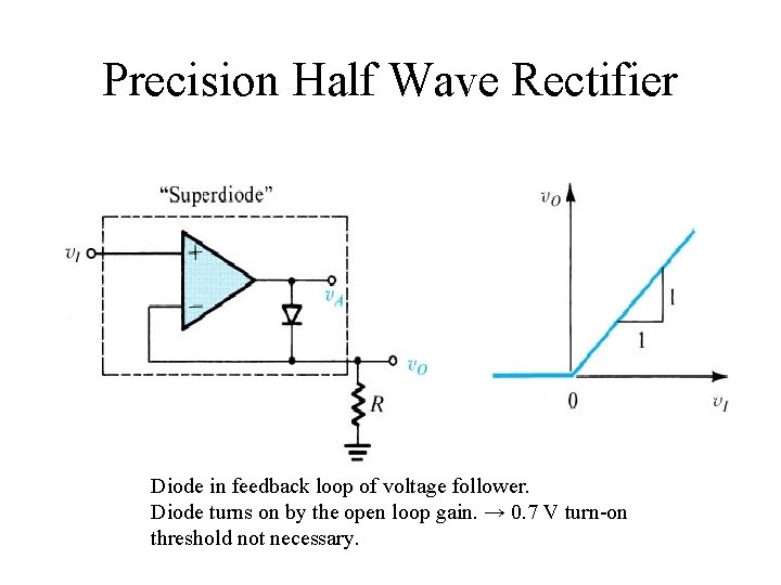
Precision Half Wave Rectifier Diode in feedback loop of voltage follower. Diode turns on by the open loop gain. → 0. 7 V turn-on threshold not necessary. Copyright 2004 by Oxford University Press, Inc.

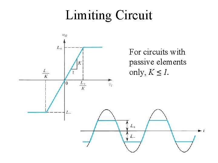
Limiting Circuit For circuits with passive elements only, K ≤ 1. Copyright 2004 by Oxford University Press, Inc.

Copyright 2004 by Oxford University Press, Inc.

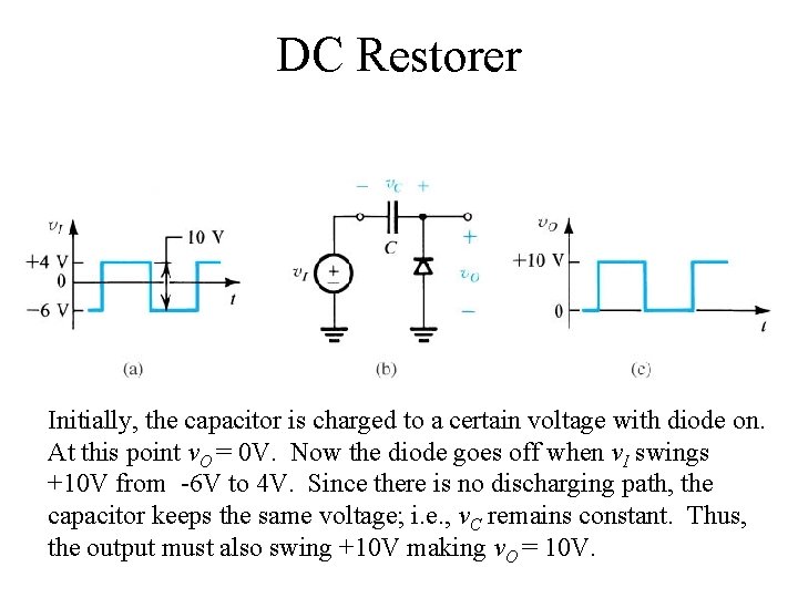
DC Restorer Initially, the capacitor is charged to a certain voltage with diode on. At this point v. O = 0 V. Now the diode goes off when v. I swings +10 V from -6 V to 4 V. Since there is no discharging path, the capacitor keeps the same voltage; i. e. , v. C remains constant. Thus, the output must also swing +10 V making v. O = 10 V. Copyright 2004 by Oxford University Press, Inc.

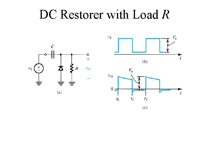
DC Restorer with Load R Copyright 2004 by Oxford University Press, Inc.

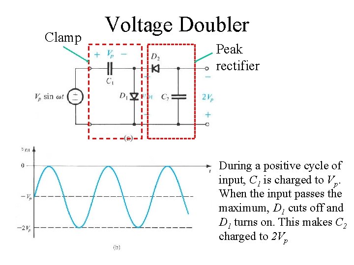
Clamp Voltage Doubler Peak rectifier During a positive cycle of input, C 1 is charged to Vp. When the input passes the maximum, D 1 cuts off and D 1 turns on. This makes C 2 charged to 2 Vp Copyright 2004 by Oxford University Press, Inc.

Special Types of Diodes • Schottky-Barrier Diode: Forward drop of 0. 3 – 0. 5 V • Varactor: Acts as a voltage variable capacitor • Photodiode: Conducts under the light in the reverse direction • Ligh Emitting Diode: Converts the forward currents to lights. Copyright 2004 by Oxford University Press, Inc.