Chapter 3 UHF RFID Antennas Figure 3 1
- Slides: 43

Chapter 3 - UHF RFID Antennas

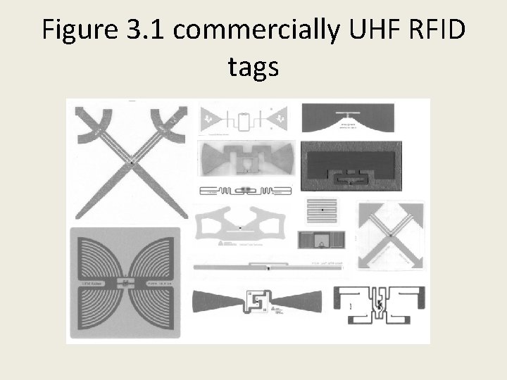
Figure 3. 1 commercially UHF RFID tags

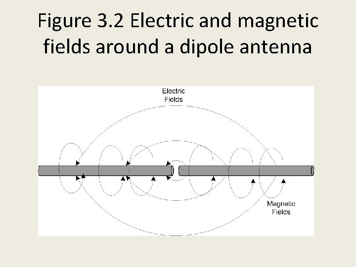
Figure 3. 2 Electric and magnetic fields around a dipole antenna

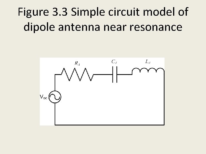
Figure 3. 3 Simple circuit model of dipole antenna near resonance

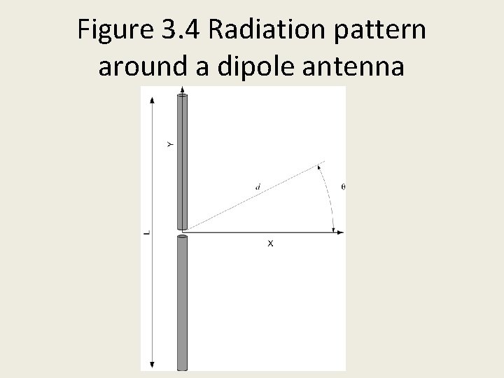
Figure 3. 4 Radiation pattern around a dipole antenna

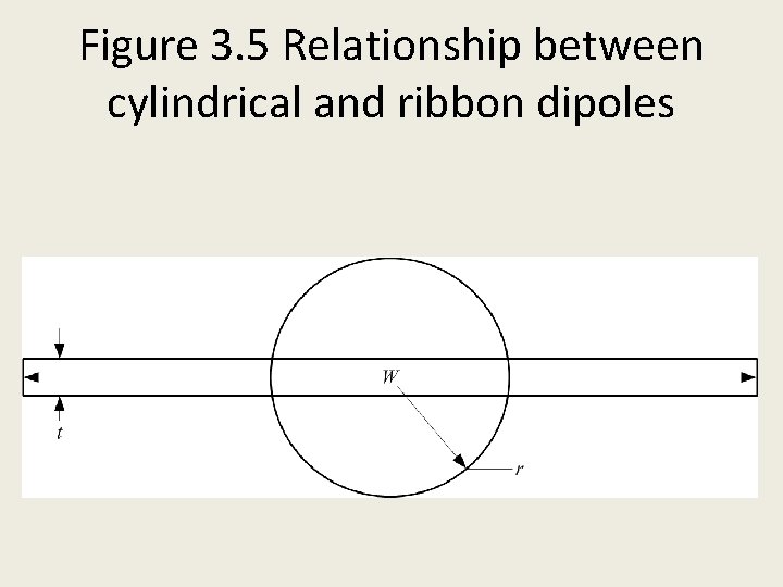
Figure 3. 5 Relationship between cylindrical and ribbon dipoles

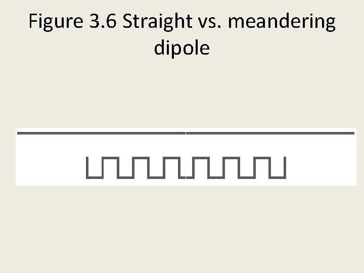
Figure 3. 6 Straight vs. meandering dipole

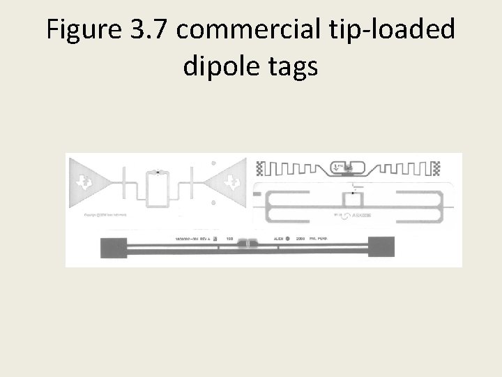
Figure 3. 7 commercial tip-loaded dipole tags

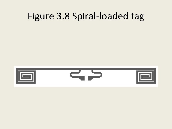
Figure 3. 8 Spiral-loaded tag

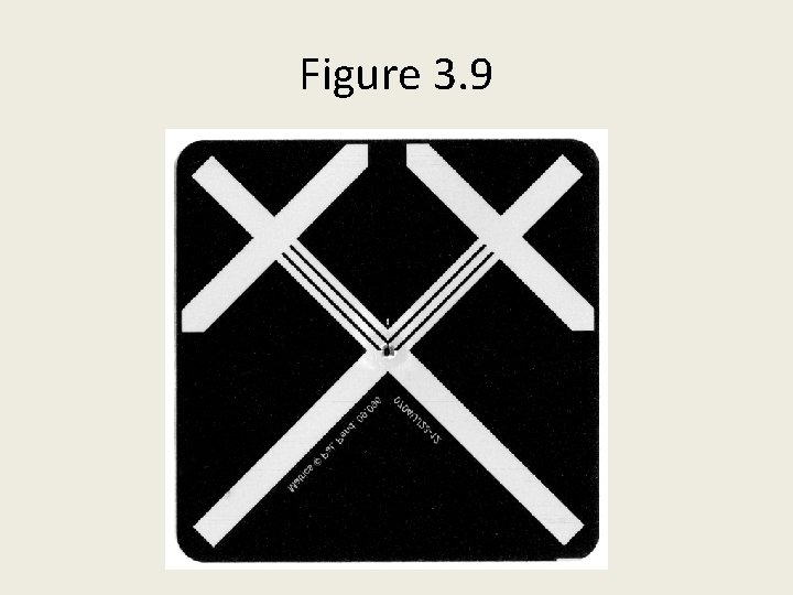
Figure 3. 9

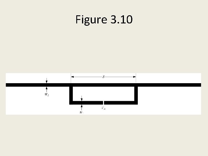
Figure 3. 10

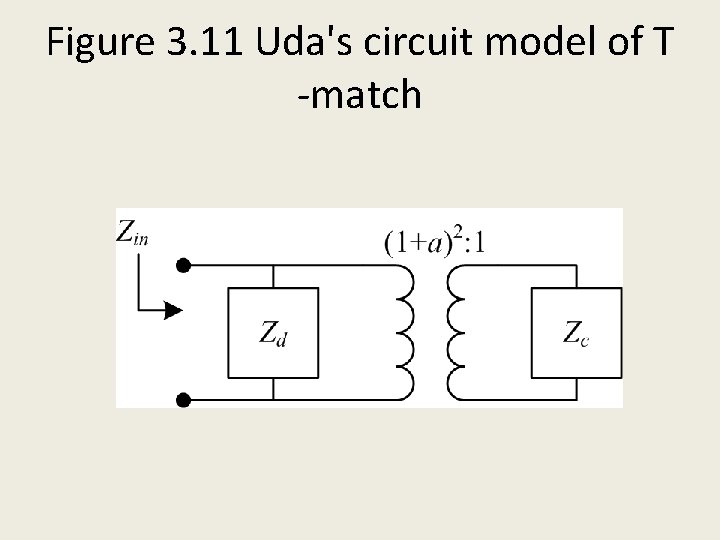
Figure 3. 11 Uda's circuit model of T -match

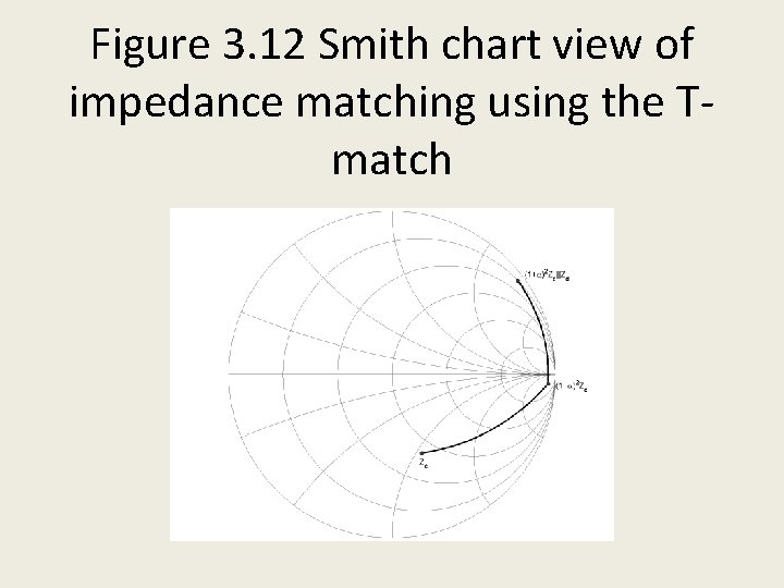
Figure 3. 12 Smith chart view of impedance matching using the Tmatch

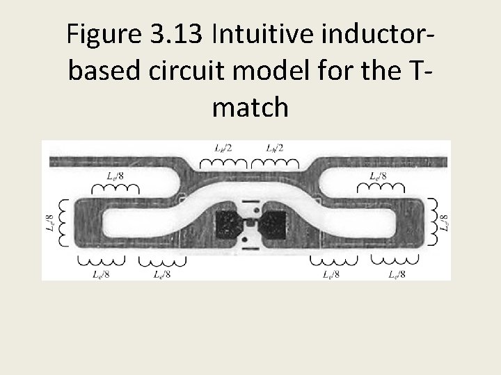
Figure 3. 13 Intuitive inductorbased circuit model for the Tmatch

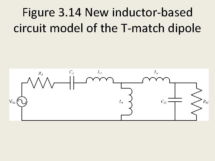
Figure 3. 14 New inductor-based circuit model of the T-match dipole

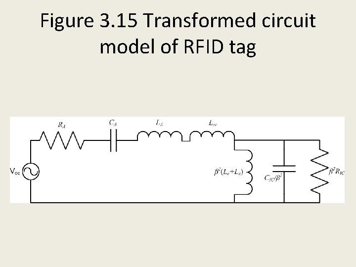
Figure 3. 15 Transformed circuit model of RFID tag

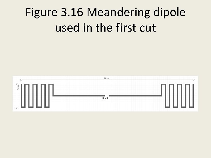
Figure 3. 16 Meandering dipole used in the first cut

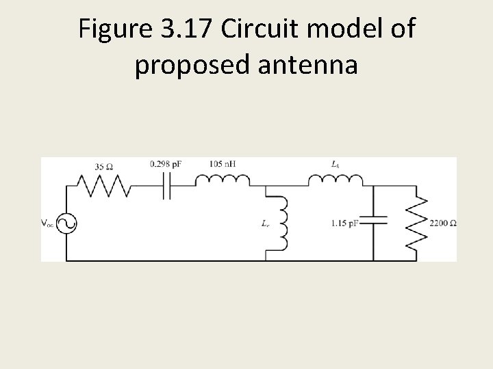
Figure 3. 17 Circuit model of proposed antenna

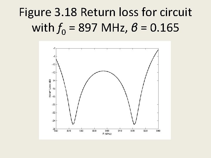
Figure 3. 18 Return loss for circuit with f 0 = 897 MHz, β = 0. 165

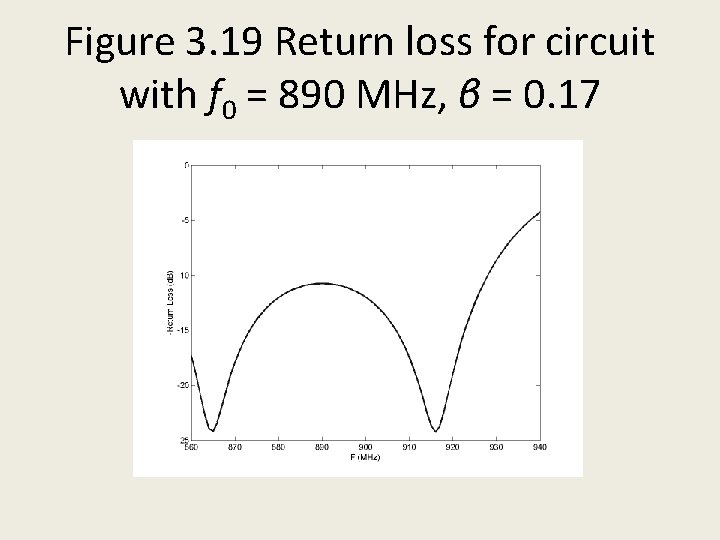
Figure 3. 19 Return loss for circuit with f 0 = 890 MHz, β = 0. 17

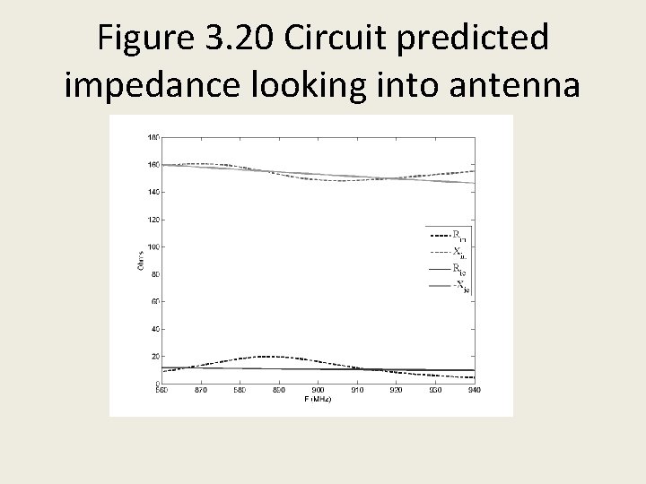
Figure 3. 20 Circuit predicted impedance looking into antenna

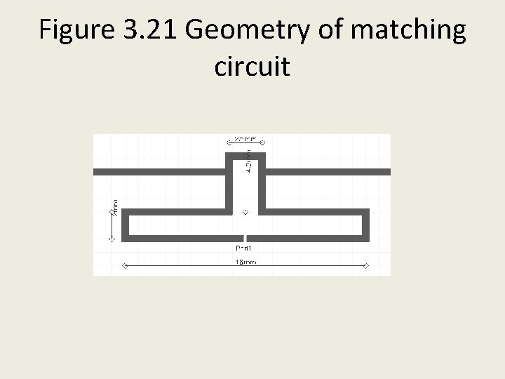
Figure 3. 21 Geometry of matching circuit

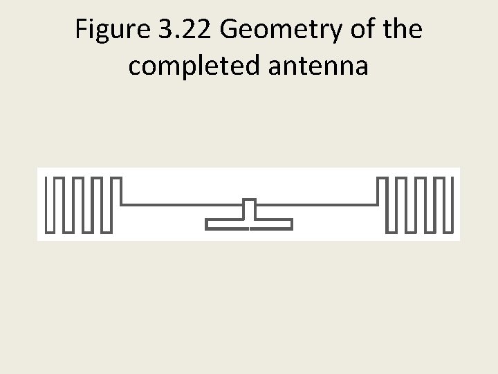
Figure 3. 22 Geometry of the completed antenna

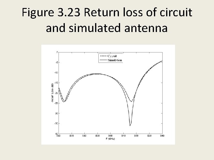
Figure 3. 23 Return loss of circuit and simulated antenna

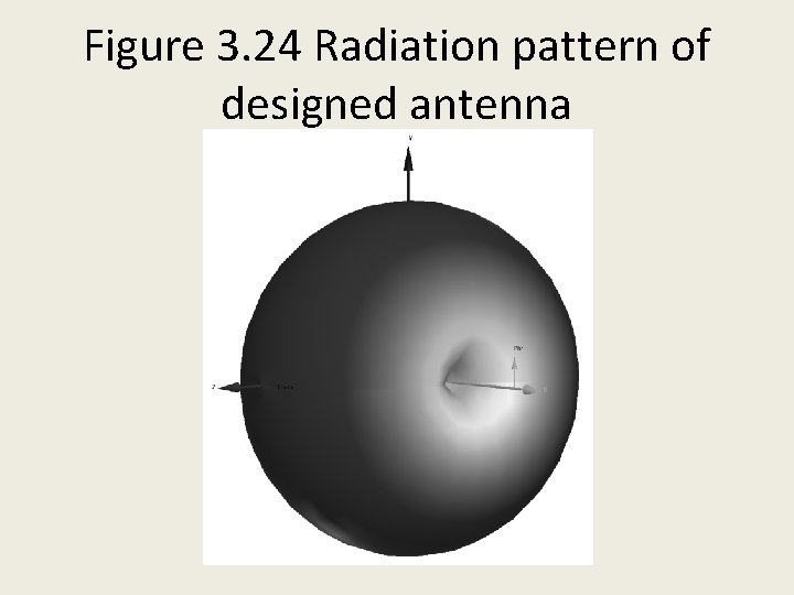
Figure 3. 24 Radiation pattern of designed antenna

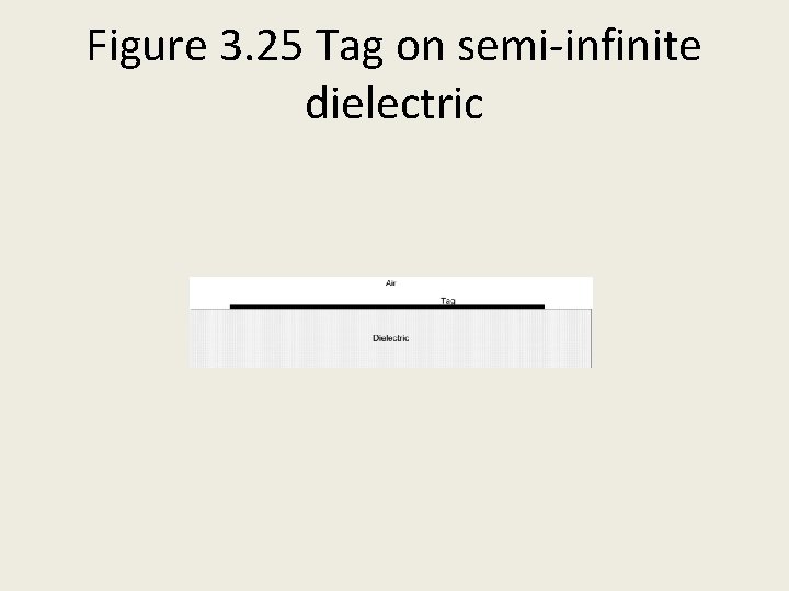
Figure 3. 25 Tag on semi-infinite dielectric

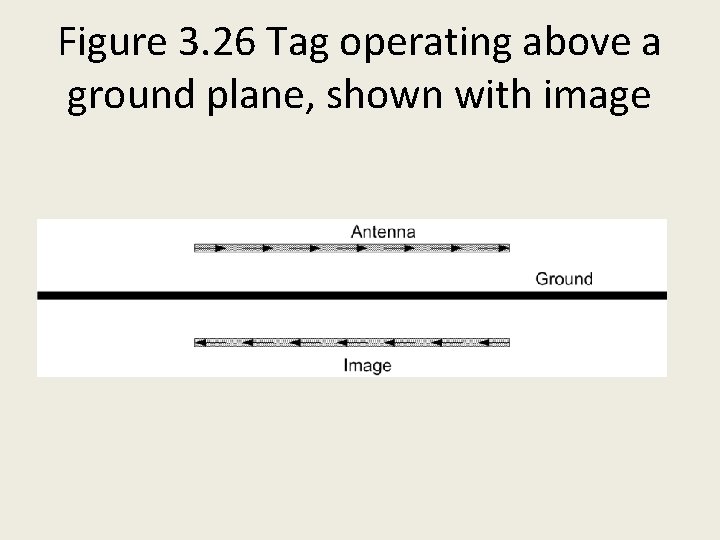
Figure 3. 26 Tag operating above a ground plane, shown with image

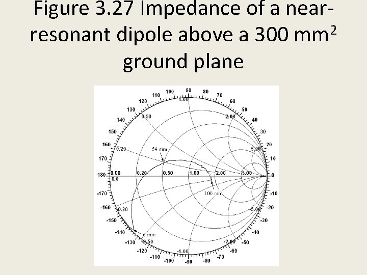
Figure 3. 27 Impedance of a nearresonant dipole above a 300 mm 2 ground plane

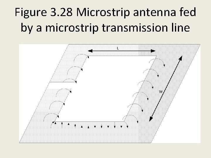
Figure 3. 28 Microstrip antenna fed by a microstrip transmission line

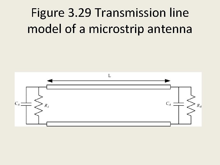
Figure 3. 29 Transmission line model of a microstrip antenna

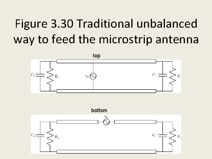
Figure 3. 30 Traditional unbalanced way to feed the microstrip antenna top bottom

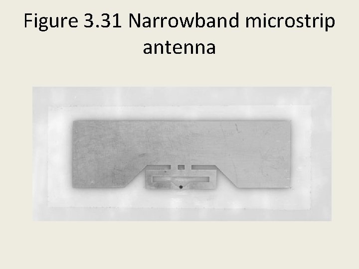
Figure 3. 31 Narrowband microstrip antenna

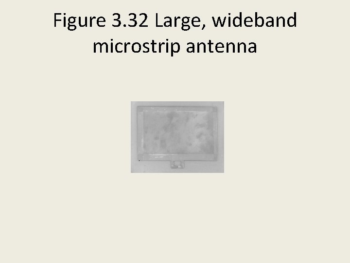
Figure 3. 32 Large, wideband microstrip antenna

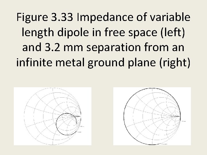
Figure 3. 33 Impedance of variable length dipole in free space (left) and 3. 2 mm separation from an infinite metal ground plane (right)

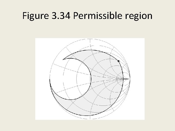
Figure 3. 34 Permissible region

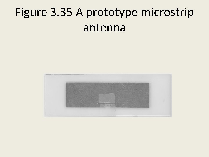
Figure 3. 35 A prototype microstrip antenna

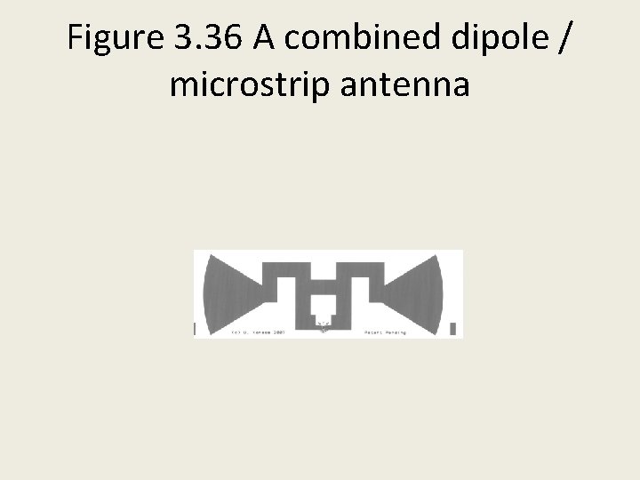
Figure 3. 36 A combined dipole / microstrip antenna

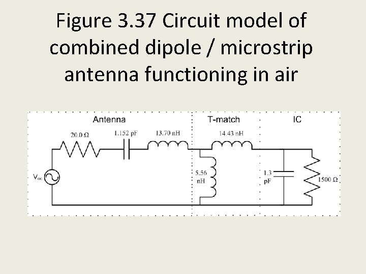
Figure 3. 37 Circuit model of combined dipole / microstrip antenna functioning in air

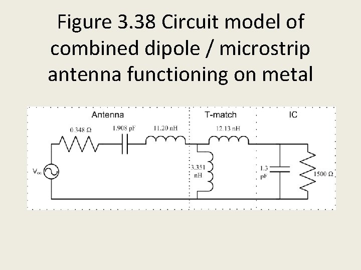
Figure 3. 38 Circuit model of combined dipole / microstrip antenna functioning on metal

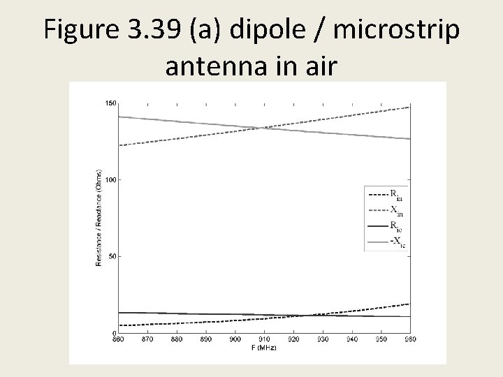
Figure 3. 39 (a) dipole / microstrip antenna in air

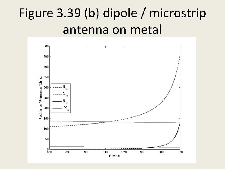
Figure 3. 39 (b) dipole / microstrip antenna on metal

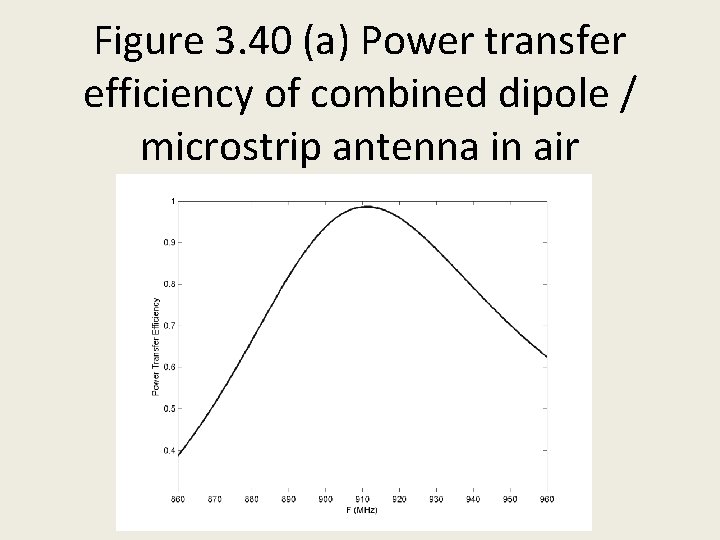
Figure 3. 40 (a) Power transfer efficiency of combined dipole / microstrip antenna in air

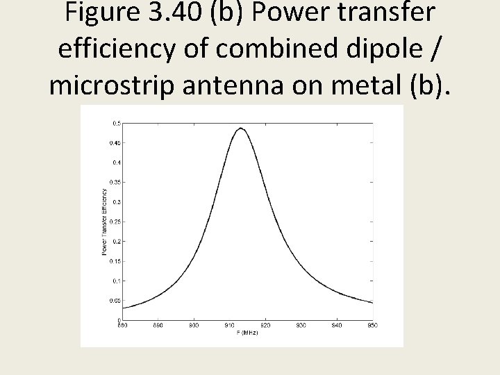
Figure 3. 40 (b) Power transfer efficiency of combined dipole / microstrip antenna on metal (b).