Atomic Force Microscope AFM STM makes use of
 • STM makes use of tunneling current It can only")


 in the SEM, magnification 1, 000 x AFM cantilever (after")


 • Tapping Mode")


- Slides: 33
Atomic Force Microscope (AFM) • STM makes use of tunneling current It can only image conducting or semiconducting surfaces • Binnig, Quate, and Gerber invented the Atomic Force Microscope in 1985 • It can image almost any type of surface, including polymers, ceramics, composites, glass, and biological samples Calvin Quate (1923) Gerd Binnig (1947) Christoph Gerber (1942)
The first Atomic Force Microscope - Science Museum London
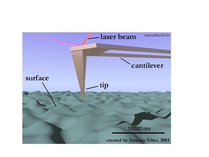
Main Components of an AFM • Cantilever with a sharp tip • Laser beam deflection system (introduced by Meyer and Amer) • Detector and Feedback electronics • Piezoelectric tube • Image display system
How It Works • • • Invented in 1986 Cantilever Tip Surface Laser Multi-segment photodetector Figure 4. Three common types of AFM tip. (a) normal tip (3 µm tall); (b) supertip; (c) Ultralever (also 3 µm tall). Electron micrographs by Jean. Paul Revel, Caltech. Tips from Park Scientific Instruments; supertip made by Jean-Paul Revel. http: //www. molec. com/what_is_afm. html http: //stm 2. nrl. navy. mil/how-afm. html#imaging%20 modes
AFM cantilever (after use) in the SEM, magnification 1, 000 x AFM cantilever (after use) in the SEM, magnification 50, 000 x AFM cantilever (after use) in the SEM, magnification 3, 000 x
The atoms of a Sodium Chloride crystal viewed with an Atomic Force Microscope
How does AFM work? Measure the forces between the sharp tip and sample surface Short-range forces Long-range forces Chemical forces: Van der Waals forces ionic bonds, covalent Capillary forces bonds, metallic bonds Magnetic forces Repulsion forces: Electrostatic force Pauli repulsion, ionic repulsion
How are forces measured? Hooke’s law: F= -ks Laser Beam Deflection Method
Fabrication of Cantilever • Made from Si₃N₄ or Si • As soft as possible to achieve high sensitivity • Spring constant < equivalent spring constant between atoms of sample in order not to dragging the atoms out of its atomic site
Fabrication of Tip • Made from Si₃N₄ or Si • As sharp as possible • The radius of curvature of the tip does not influence the height of a feature but the lateral resolution
Modes of Imaging Constant Height • Cantilever is "dragged" across the surface of the sample • Tip is free to move up and down • Force between tip and sample surface is measured directly using the deflection of the cantilever üNo need to wait for the response of feedback system, scan in high speed üNo signal error x If surface is rough, can cause damage to tip and surface
Modes of Imaging Constant Force • Move the cantilever up and down using the piezoelectric tube • so that the position of laser beam is unchanged • i. e. force between tip and sample surface remain constant üSuited for almost every surface x Scan slowly, need to wait for the response of feedback system x Sensitive to random noise, has signal error
Constant Force Modes • Contact Mode (<0. 5 nm tip-surface separation) • Tapping Mode (0. 5 -2 nm tip-surface separation) • Non-contact Mode (0. 1 -10 nm tip-surface separation)
Topography • Contact Mode – High resolution – Damage to sample – Can measure frictional forces • Non-Contact Mode – Lower resolution – No damage to sample • Tapping Mode – Better resolution – Minimal damage to sample 2. 5 x 2. 5 nm simultaneous topographic and friction image of highly oriented pyrolytic graphic (HOPG). The bumps represent the topographic atomic corrugation, while the coloring reflects the lateral forces on the tip. The scan direction was right to left http: //stm 2. nrl. navy. mil/how-afm. html#imaging%20 modes
Contact Mode • Tip almost touches the surface • Force on the tip is repulsive • Force between the tip and the surface is kept constant during scanning by maintaining a constant deflection Advantages: ü Better resolution than tapping mode and non-contact mode ü Fast scanning ü Good for rough surface Disadvantages: x Force can damage or deform soft samples
Tapping Mode • Cantilever is driven to oscillated up and down at its resonant frequency • Probe slightly taps on the surface during scanning, contacting the surface at the bottom of its swing • Adjust the height of cantilever by the piezoelectric tube to maintain a constant oscillation amplitude i. e. constant force between tip and surface is maintained Advantages: üHigh resolution for the samples that are easily damaged (biological sample) Disadvantages: x Slower scanning speed needed
Non-contact Mode • Tip does not contact the surface • Similar to tapping mode, cantilever is oscillated at its resonant frequency • Adjust height of cantilever to keep constant oscillation amplitude, constant force between tip and surface Advantages: ü Prevent tip from sticking to the surface (Note: all samples unless in a controlled UHV or environmental chamber have some liquid adsorbed on the surface). ü Low force exerted on surface ü No damage to tip and surface Disadvantages: x Lower resolution x Slower speed
Applications • Biological Science : Live cell Human Lung Cancer Scan size: 60 µCell m
Applications • • Materials Science DVD Polymer Science Data Storage : Help in design hard disk drive at nanoscale level Semi conductor Surface topography of Zn. O film Image of polymer blend
Lateral Force Microscopy • The probe is scanned sideways. The degree of torsion of the cantilever is used as a relative measure of surface friction caused by the lateral force exerted on the probe. • Identify transitions between different components in a polymer blend, in composites or other mixtures • This mode can also be used to reveal fine structural details in the sample.
Lateral Force Microscopy Images/photo taken with Nano. Scope® SPM, courtesy Digital Instruments, Santa Barbara , CA Natural rubber/ EDPM blend 20 micron scan Polished polycrystalle silicon carbide film. Grain structures 30 micron scan Magnetic recording head Al oxide grains and contamination
Phase Imaging • Accessible via Tapping. Mode • Oscillate the cantilever at its resonant frequency. The amplitude is used as a feedback signal. The phase lag is dependent on several things, including composition, adhesion, friction and viscoelastic properties. l l l Identify two-phase structure of polymer blends Identify surface contaminants that are not seen in height images Less damaging to soft samples than lateral force microscopy
Phase Imaging Image/photo taken with Nano. Scope® SPM, courtesy Digital Instruments, Santa Barbara , CA Compositepolymer imbedded in a matrix 1 micron scan Bond pad on an integrated circuit Contamination 1. 5 micron scan Mo. O 3 crystallites on a Mo. S 2 substrate 6 micron scan
Magnetic Force Microscopy • Special probes are used for MFM. These are magnetically sensitized by sputter coating with a ferromagnetic material. • The cantilever is oscillated near its resonant frequency (around 100 k. Hz). • The tip is oscillated 10’s to 100’s of nm above the surface • Gradients in the magnetic forces on the tip shift the resonant frequency of the cantilever. • Monitoring this shift, or related changes in oscillation amplitude or phase, produces a magnetic force image. • Many applications for data storage technology
Magnetic Force Microscopy Image/photo taken with Nano. Scope® SPM, courtesy Digital Instruments, Santa Barbara , CA Overwritten tracks on a textured hard disk, 25 micron scan Domains in a 80 micron garnet film
Force Modulation Imaging • Oscillate the cantilever vertically at a rate that is significantly faster than the scan rate. • The amplitude of the oscillations changes in response to the sample stiffness. • Used in conjunction with Lift. Mode to separate topography and elasticity data.
Force Modulation Imaging
Other Techniques Image/photo taken with Nano. Scope® SPM, courtesy Digital Instruments, Santa Barbara , CA • Scanning capacitance microscopy – Apply a constant amplitude sine wave voltage to the sample. The image is then reconstructed from the changes in the amplitude of the capacitance oscillations. – Location of defects in wafers (pinning of electrical carriers) – Image carrier concentration • Scanning thermal microscopy – Uses a temperature sensitive probe with a special holder. – Location of “hot-spot” defects in semiconductor wafers 90 micron scan size
Other Techniques • Nanoindenting and scratching – A diamond tip is mounted on a metal cantilever and scanned either with contact or Tapping. Mode. – Indenting mode presses the tip into the sample – Scratch mode drags the tip across the sample at a specific rate and with a specified force. – The use of Tapping. Mode makes it possible to simultaneously image soft samples. • Imaging of biological samples – cells, DNA (Tapping. Mode in solution)
Reference • • Wikipedia – Scanning Tunneling Microscope http: //en. wikipedia. org/wiki/Scanning_tunneling_microscope Atomic Force Microscope http: //en. wikipedia. org/wiki/Atomic_force_microscope http: //ww. parkafm. com/ Atomic Force Microscopy lecture notes by Hui. Wen Cheng Introduction to Scanning Probe Microscopy (SPM), Basic Theory, Atomic Force Microscopy (AFM) by Robert A. Wilson and Heather A. Bullen, Department of Chemistry, Northern Kentucky University, Highland Heights, KY 41099.