Imaging at nanoscale using AFM and SEM SUBMITTED

Imaging at nano-scale using AFM and SEM SUBMITTED BY: SUPERVISOR: SOUMITA CHAKRABORTY DR. SYED ARSHAD HUSSAIN ASST. PROFESSOR DEPARTMENT OF PHYSICS NABANITA SARKAR

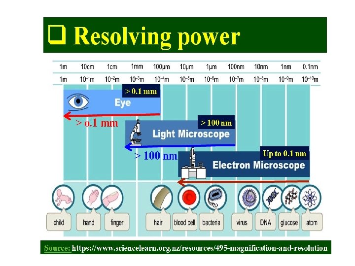
THE SENSE OF SEEING IS VERY IMPORTANT FOR HUMAN BEINGS. WE CAN HAVE A BETTER IDEA ABOUT ANYTHING JUST BY SEEING INSTEAD OF HEARING OR TOUCHING. HERE WE CAN SEE THAT JUST BY SEEING THE PICTURE WE ARE ABLE TO DISTINGUISH WHO THEY ARE WHICH WOULD BE A LITTLE DIFFICULT TO UNDERSTAND BY VERBAL DESCRIPTION. SO WE CAN SAY THAT WE NEED TO SEE THINGS FOR BETTER UNDERSTANDING. BUT HUMAN EYE HAS SOME LIMITATIONS. FOR SEEING OBJECTS MUCH SMALLER THAN THE CAPABILITY OF HUMAN EYE, WE NEED SPECIAL MICROSCOPES.

OPTICAL MICROSCOPE Ø. The magnification of a optical microscope with visible light is about 1250× and theoretical limit of resolution is 250 nanometres. ØAny object which is smaller than the half the wavelength of light which is used in an optical microscope, could not be visible by the optical microscope. Ø. So for an object below the length of 200 nm, the microscope is not useful. To study smaller object less than 200 nm, special arrangement is required. ØAFM and SEM are used for imaging these smaller objects.

PART 1: ATOMIC FORCE MICROSCOPY

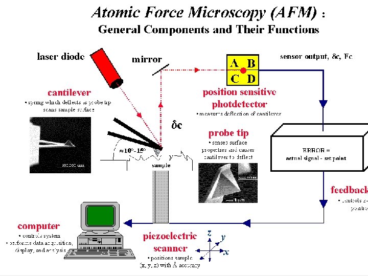
THE PRINCIPLE BEHIND THE MICROSCOPIC TECHNIQUE IS THAT IN THIS METHOD A LASER BEAM IS FOCUSED ON THE BACK OF A CANTILEVER THAT MOVES UP AND DOWN ON THE SURFACE OF A SPECIMEN AND THE DEFLECTIONS OF THE BEAM ARE CAPTURED BY A DIODE.

SCANNING MODES: CONTACT MODE THREE MODES: NON CONTACT MODE TAPPING MODE

CONTACT MODE: Tip always touches the sample Force on the tip is repulsive Force between the tip and the surface is kept constant during scanning by maintaining a constant deflection ADVANTAGES: §Better resolution than tapping mode and non contact mode. §Fast scanning. §Good for rough surface. DISADVANTAGES: §Tip breakage, surface sensitivity. §Not suitable for soft samples

Tip does not contact the surface Cantilever is oscillated at its resonant frequency Adjust height of cantilever to keep constant oscillation amplitude, constant force between tip and surface Advantages: §Prevent tip from sticking to the surface. §Low force exerted on the surface §No damage to tip and surface Disadvantages: §Lower resolution §Slow speed

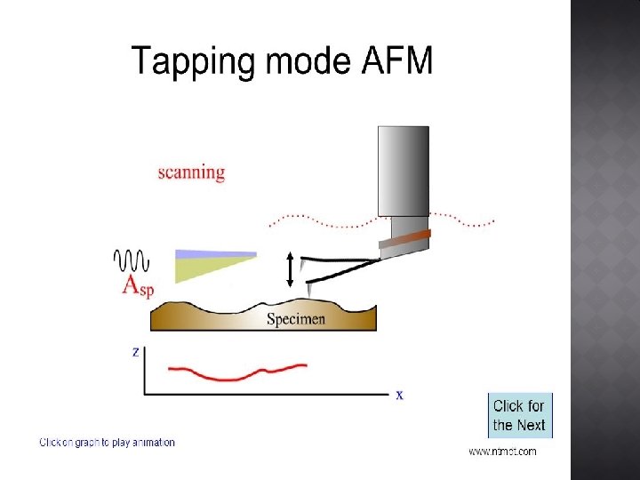
Cantilever is driven to oscillated up and down at its resonant frequency Probe slightly taps on the surface during scanning, contacting the surface at the bottom of the swing. Adjust the height of cantilever by the piezoelectric tube to maintain a constant oscillation amplitude i. e constant force between tip and surface is maintained. Advantages: High resolution for the samples that are easily damaged (biological samples) Disadvantages: Slower scanning speed.

APPLICATIONS Materials investigated: • Thick and thin film coating, ceramics, composites, glasses, synthetic and biological membranes, metals, polymers and semiconductors. Used to study phenomenon of: • Abrasion, adhesion, cleaning, corrosion, , etching, friction, lubricating, plating and polishing Measure : • AFM can image surface of material in atomic resolution and also measure force at a nano Newton scale.
: TYPICALLY USED FOR SCANNING AND STUDING")
ADVANCED IMAGING TECHNIQUES: Ø MAGNETIC FORCE MICROSCOPY (MFM): TYPICALLY USED FOR SCANNING AND STUDING SURFACES WITH MAGNETIC PROPERTIES. Ø ELECTROSTATIC FORCE MICROSCOPY (EFM): USED FOR MEASURING ELECTROSTATIC FORCE BETWEEN THE SURFACE AND THE AFM CANTILEVER. IMAGE GIVES INFORMATION ABOUT SURFACE POTENTIAL AND CHARGE DISTRIBUTION OF A SAMPLE SURFACE. Ø SCANNING THERMAL MICROSCOPE(STh. M): MAPS THE LOCAL TEMPERATURE AND THERMAL CONDUCTIVITY OF AN INTERFACE. Ø CONDUCTIVE AFM(C-AFM): MEASURES THE TOPOGRAPHY OF A MATERIAL AND THE ELECTRIC CURRENT FLOW AT THE CONTACT POINT OF THE TIPWITH THE SURFACE OF THE SAMPLE
 MFM IMAGE OF")
TOPOGRAPHIC AND CURRENT MAPS OF POLYCRYSTALLINE Hf. O 2 STACK (C-AFM) MFM IMAGE OF HARD DISK STh. M IMAGE OF OPTICAL FIBRE IN EPOXY EFM PHASE IMAGE OF THE PZT FILM BY ENHANCED EFM
 v. LIMITED SCANNING AREA(150 X 150")
LIMITATIONS: v. LIMITED VERTICAL RANGE (10 -20 MICROMETERS) v. LIMITED SCANNING AREA(150 X 150 MICROMETERS) v. DATA IS NOT INDEPENDENT OF TIP v. TIP OR SAMPLE CAN BE DAMAGED v. LIMITED SCANNING SPEED

PART 2: SCANNING ELECTRON MICROSCOPE

OVERVIEW A SCANNING ELECTRON MICROSCOPE IS A TYPE OF ELECTRON MICROSCOPE THAT IMAGES A SAMPLE BY SCANNING IT WITH A HIGH ENERGY BEAM OF ELECTRONS IN A RASTER SCAN PATTERN. THE ELECTRONS INTERACT WITH THE ATOMS THAT MAKE UP THE SAMPLE PRODUCING SIGNALS THAT CONTAIN INFORMATION ABOUT THE SAMPLE SURFACE TOPOGRAPHY, COMPOSITION AND OTHER PROPERTIES.

PRINCIPLE: Ø Ø The basic principle is that a beam of electrons is generated by a suitable source, typically a tungsten filament or a field emission gun. The electron beam is accelerated through a high voltage and pass through a system of aperture and electromagnetic lenses to produce a thin beam of electrons. When the accelerated primary electrons strikes the sample, then the surface of the specimen it produces secondary electrons. These secondary electrons are collected by a positive charged electron detector which in turn gives a 3 dimensional image of the sample.

SCHEMATIC DIAGRAM OF A TYPICAL SEM

CONSTRUCTION THE BASIC COMPONENTS ARE AS FOLLOWING: 1. Condenser lenses 2. Electron gun 3. Objective aperture 1. Scan coils 2. Chamber( specimen test) 3. Detector 4. Computer hardware and software

When the beam touches the surface of the sample it produces 1. secondary electrons 2. back scattered electrons 3. X- Rays. v. Secondary electrons are low energy electrons formed by low energy scattering. v Electrons are collected by placing a positive grill on the front of the SE detector. v. The positive grill attracts negative electrons and they go through it into the detector. v. Everhart – Thornley Detector is commonly used
 detects elastically scattered electrons. This BSE are used")
v. A backscatter electron detector (BSD) detects elastically scattered electrons. This BSE are used to form different kind of image. v. Such an image uses contrast to tell us about the average atomic number of the sample. SCHEMETIC OF FOUR QUADRANT BACKSCATTERED ELECTRON DETECTOR v. In scanning electron microscopy, an x-ray is emitted when the electron beam displaces an inner shell electron that is replaced by an outer shell electron. v Because each element has a unique energy difference between outer and inner electron shells, the x-rays that are detected yield an elemental identification over an area.
 scanning electron ― This is the most common type")
1. Conventional microscopy: (high vacuum) scanning electron ― This is the most common type of machine ― It requires a dry, conductive sample ― The sample must be able to withstand high vacuum 2. Variable pressure or low vacuum scanning electron microscopy (LVSEM): ― This type of machine has the advantage of low vacuum mode(LV) that the sample can be adjusted in the sample chamber. ― Used to image the surface of non conductive samples. ― Particularly used for viewing polymers, biological samples, museum samples, particulate samples and geological materials.
: ―Used to view samples in frozen state. ―This")
3. Cryo- scanning electron microscope (Cryo-SEM): ―Used to view samples in frozen state. ―This is particularly useful for viewing hydrated(wet) samples, delicate biological samples, hydrogels, food, biofilms, foams, fats, waxes, suspensions, pharmaceuticals, and nano particles. 4. Environmental scanning electron microscope(ESEM): ―Used to view the sample in its natural state. ―Sample temperature and specimen chamber vapour pressure can both be controlled allowing samples to be heated, cold, wetted or dried. ―Imaging of biological processes, for example pollen tube growth in real time through wetting of pollen.

APPLICATIONS SEM IS ONE OF THE MOST VERSATILE TECHNIQUE AND CAN BE USED TO: 1. IMAGE MORPHOLOGY OF SAMPLES 2. IMAGE COMPOSITIONAL AND SOME BONDING DIFFERENCES 3. EXAMINE WET AND DRY SAMPLES WHILE VIEWING THEM 4. VIEW FROZEN MATERIAL 5. GENERATE X-RAY FROM SAMPLES FOR MICROANALYSIS 6. VIEW/MAP GRAIN ORIENTATION/CRYSTALLOGRAPHIC ORIENTATION AND STUDY RELATED INFORMATION LIKE HETERIGENEITY.
 IN LUNG TISSUE SKIN TISSUE")
BONE OF A BIRD ALVEOLAR MACROPHAGES (GREY) IN LUNG TISSUE SKIN TISSUE

DISADVANTAGES 1. The disadvantages of scanning electron microscope starts with the size and cost. 2. SEMs are expensive, large and must be housed in an area free of possible electric, magnetic or vibration interference. 3. Sample must be made conductive. 4. Special training is required to operate SEM and prepare samples. 5. SEMs carry a small risk of radiation exposure associated with the electrons that scatter from beneath the sample surface.

In this project we have studied about the two imaging instruments AFM & SEM, which is used to observe substances at nano dimension. We have also deposited a thin film of clay-hectorite using spin coating technique and produce images under AFM. As ordinary optical microscope has many limitation on imaging at nano scale so these instruments are so powerful tools in this regime. These are extremely useful for scientists and researchers from all over the world and in many different branches (medical, forensic, biological, industrial work) who wants to measure incredibly small samples with great degree of accuracy.

- Slides: 30