Analytic expressions for time resolution of silicon pixel
- Slides: 38

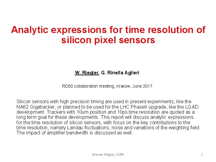
Analytic expressions for time resolution of silicon pixel sensors W. Riegler, G. Rinella Aglieri RD 50 collaboration meeting, Krakow, June 2017 Silicon sensors with high precision timing are used in present experiments, like the NA 62 Gigatracker, or planned to be used for the LHC Phase. II upgrade, like the LGAD development. Trackers with 10 um position and 10 ps time resolution are quoted as a long term goal for these developments. This report will discuss analytic expressions for the time resolution of silicon sensors, with focus on the key contributions to the time resolution, namely Landau fluctuations, noise and variations of the weighting field. The impact of amplifier bandwidth is discussed as well. Werner Riegler, CERN 1

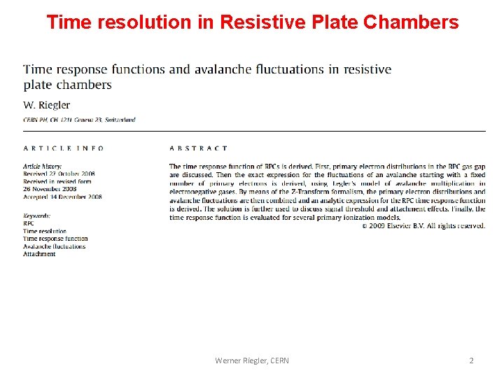
Time resolution in Resistive Plate Chambers Werner Riegler, CERN 2

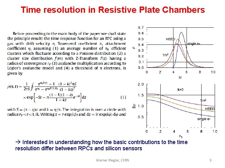
Time resolution in Resistive Plate Chambers Interested in understanding how the basic contributions to the time resolution differ between RPCs and silicon sensors Werner Riegler, CERN 3

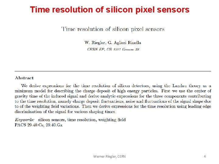
Time resolution of silicon pixel sensors Werner Riegler, CERN 4

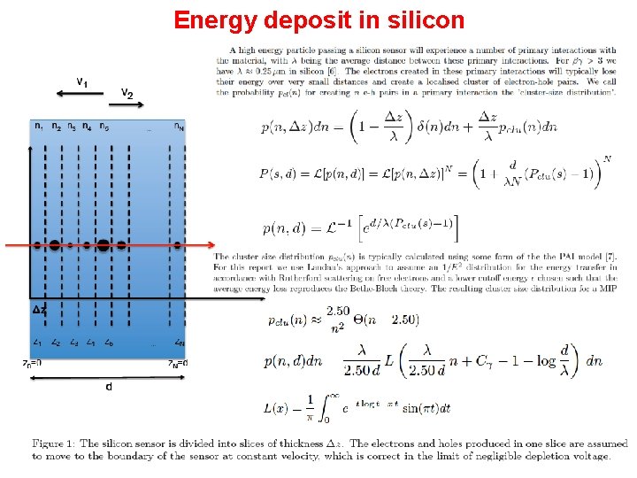
Energy deposit in silicon Werner Riegler, CERN 5

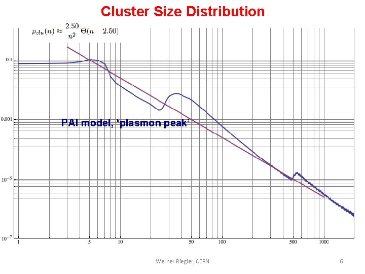
Cluster Size Distribution PAI model, ‘plasmon peak’ Werner Riegler, CERN 6

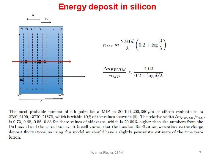
Energy deposit in silicon Werner Riegler, CERN 7

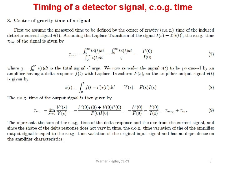
Timing of a detector signal, c. o. g. time Werner Riegler, CERN 8

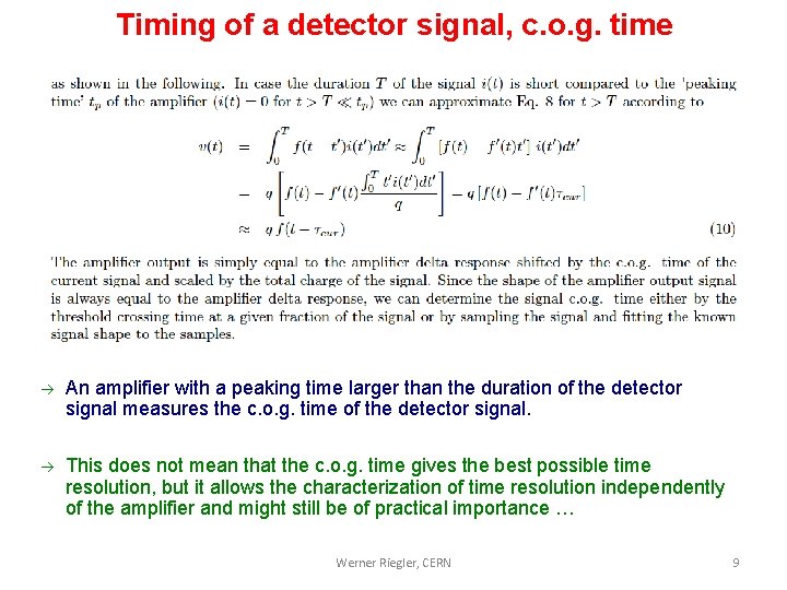
Timing of a detector signal, c. o. g. time An amplifier with a peaking time larger than the duration of the detector signal measures the c. o. g. time of the detector signal. This does not mean that the c. o. g. time gives the best possible time resolution, but it allows the characterization of time resolution independently of the amplifier and might still be of practical importance … Werner Riegler, CERN 9

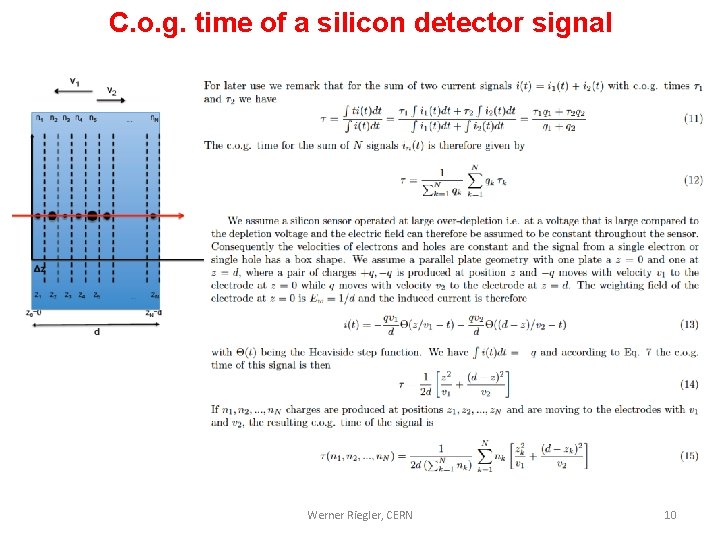
C. o. g. time of a silicon detector signal Werner Riegler, CERN 10

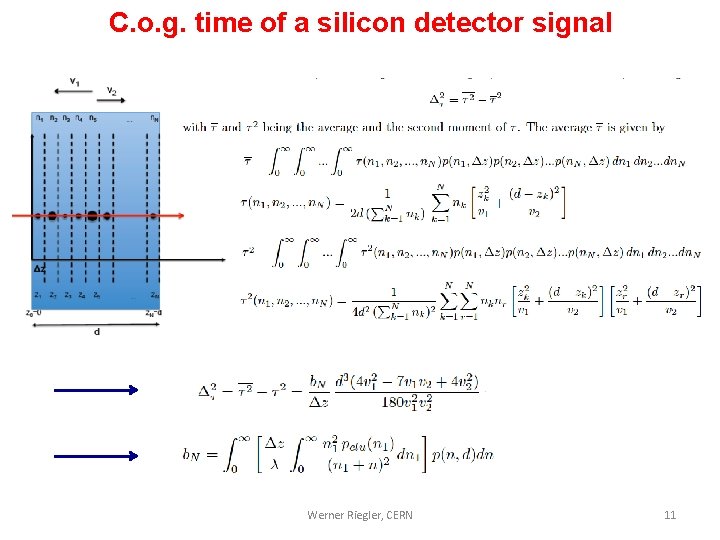
C. o. g. time of a silicon detector signal Werner Riegler, CERN 11

C. o. g. time of a silicon detector signal Werner Riegler, CERN 12

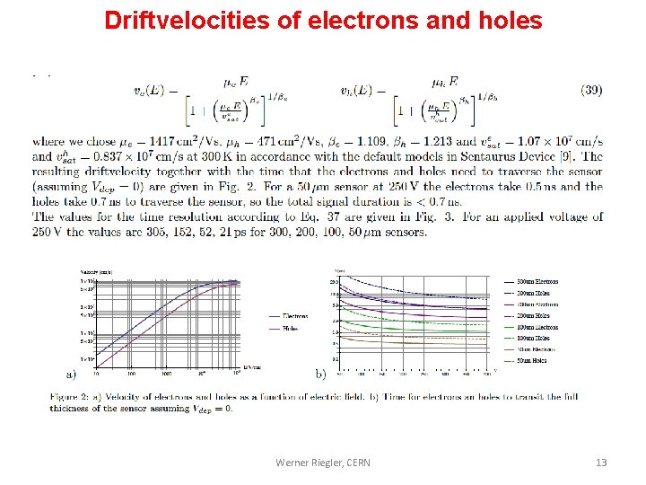
Driftvelocities of electrons and holes Werner Riegler, CERN 13

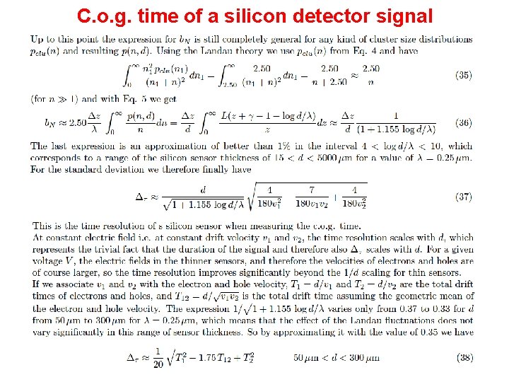
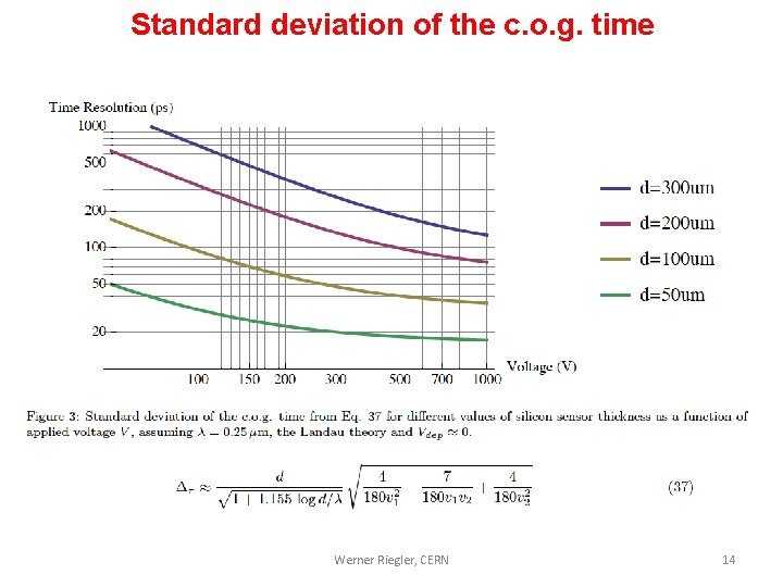
Standard deviation of the c. o. g. time Werner Riegler, CERN 14

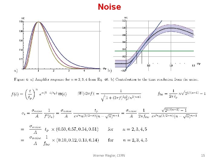
Noise Werner Riegler, CERN 15

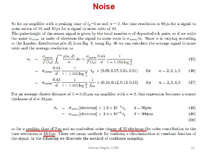
Noise Werner Riegler, CERN 16

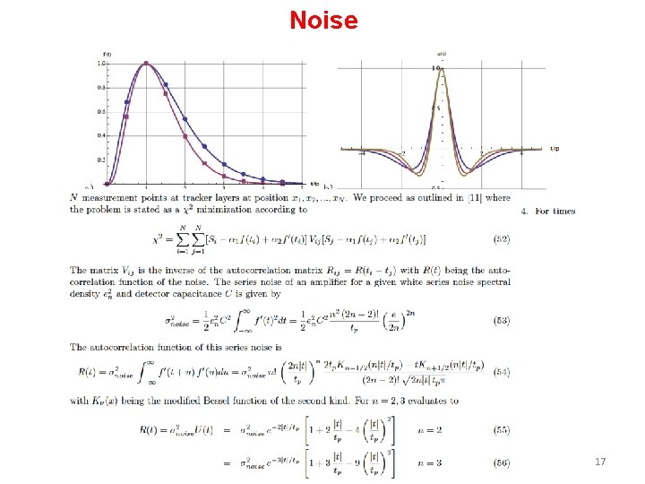
Noise Werner Riegler, CERN 17

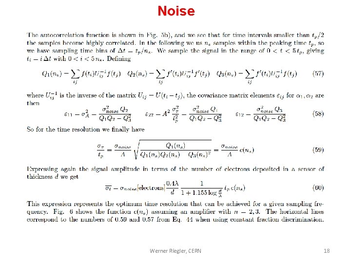
Noise Werner Riegler, CERN 18

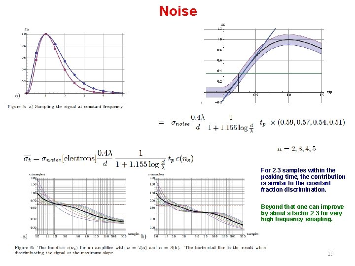
Noise For 2 -3 samples within the peaking time, the contribution is similar to the cosntant fraction discrimination. Beyond that one can improve by about a factor 2 -3 for very high frequency smapling. Werner Riegler, CERN 19

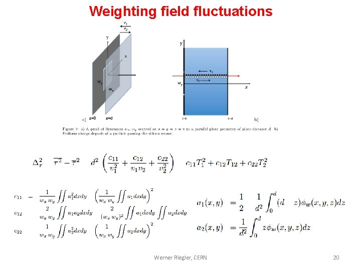
Weighting field fluctuations Werner Riegler, CERN 20

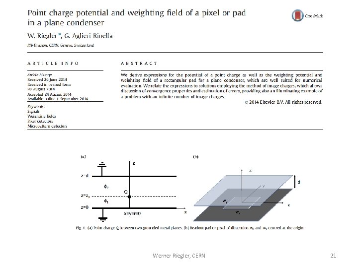
Werner Riegler, CERN 21

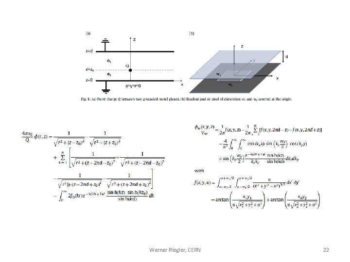
Werner Riegler, CERN 22

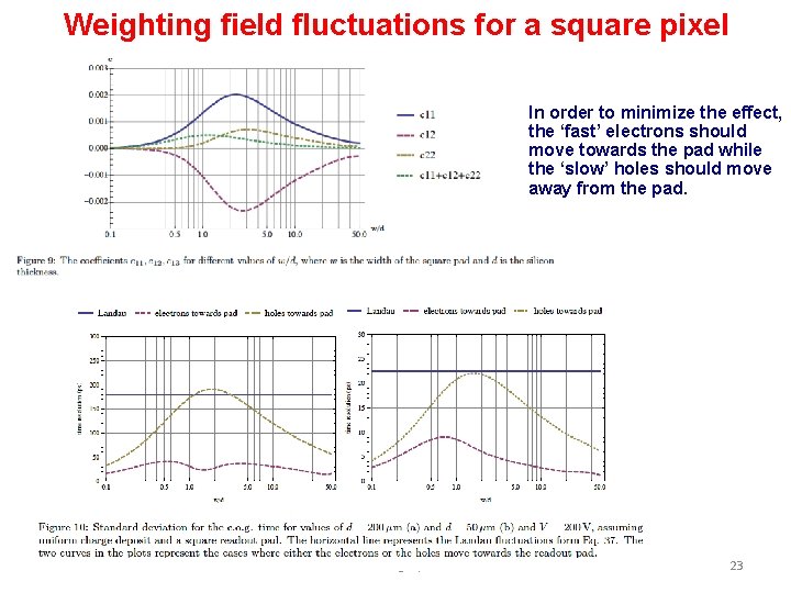
Weighting field fluctuations for a square pixel In order to minimize the effect, the ‘fast’ electrons should move towards the pad while the ‘slow’ holes should move away from the pad. Werner Riegler, CERN 23

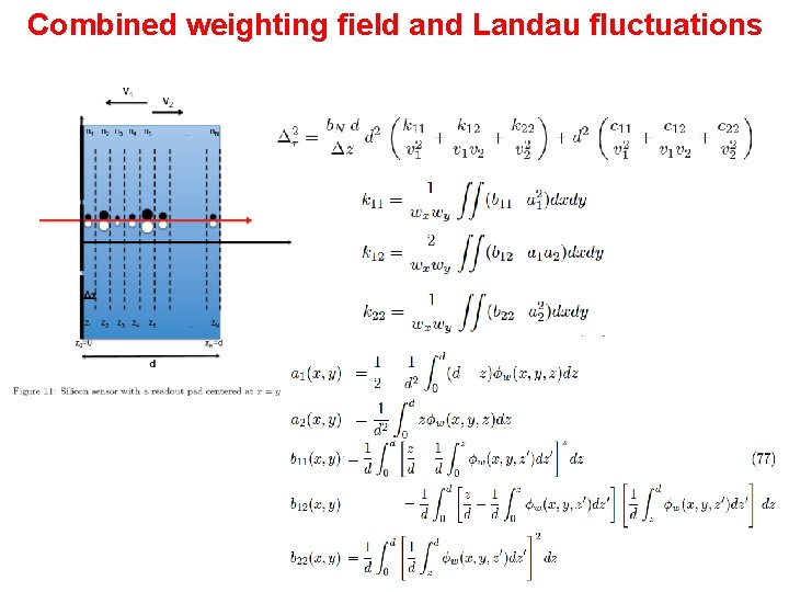
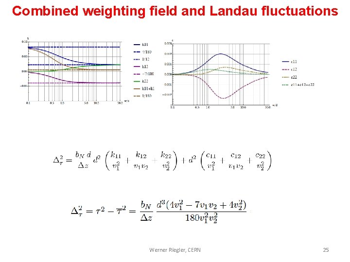
Combined weighting field and Landau fluctuations Werner Riegler, CERN 24

Combined weighting field and Landau fluctuations Werner Riegler, CERN 25

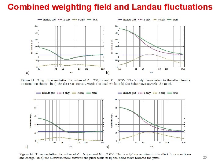
Combined weighting field and Landau fluctuations Werner Riegler, CERN 26

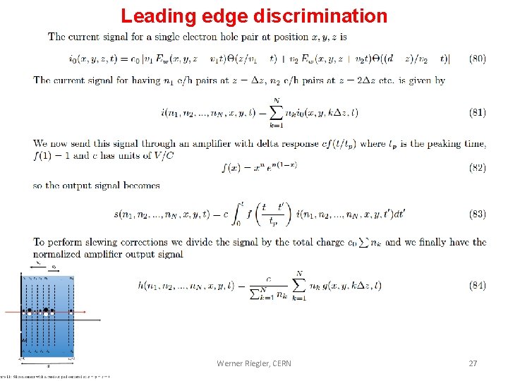
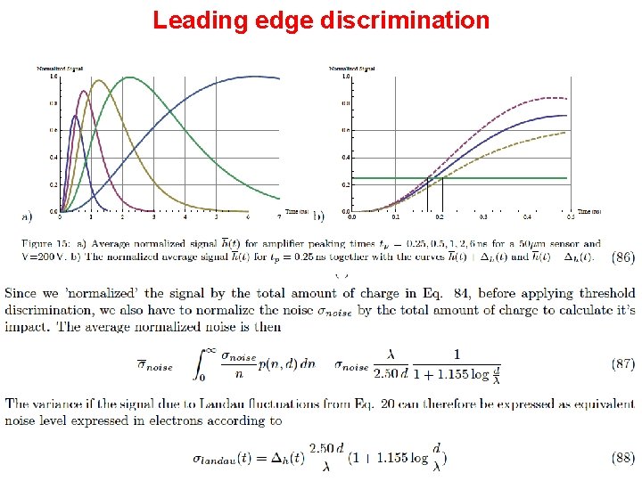
Leading edge discrimination Werner Riegler, CERN 27

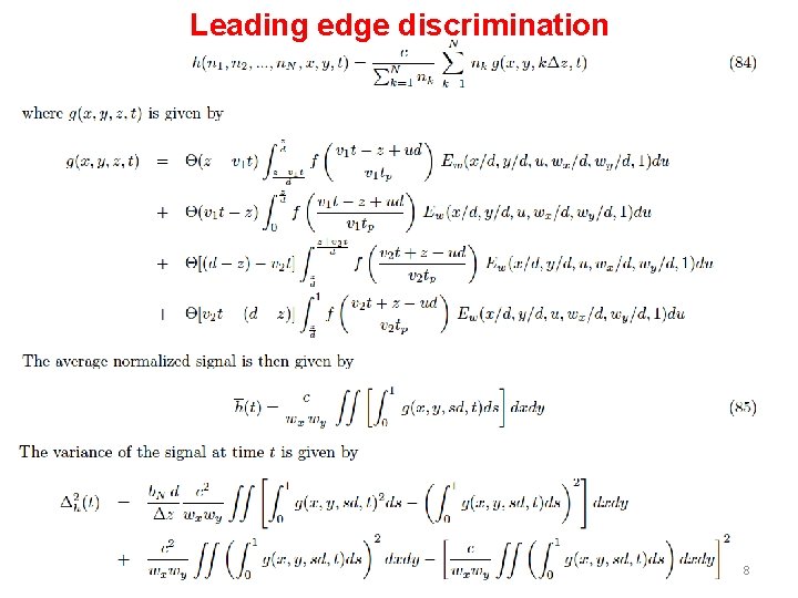
Leading edge discrimination Werner Riegler, CERN 28

Leading edge discrimination Werner Riegler, CERN 29

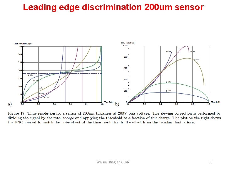
Leading edge discrimination 200 um sensor Werner Riegler, CERN 30

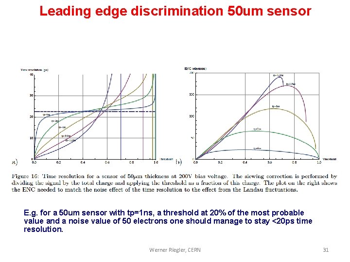
Leading edge discrimination 50 um sensor E. g. for a 50 um sensor with tp=1 ns, a threshold at 20% of the most probable value and a noise value of 50 electrons one should manage to stay <20 ps time resolution. Werner Riegler, CERN 31

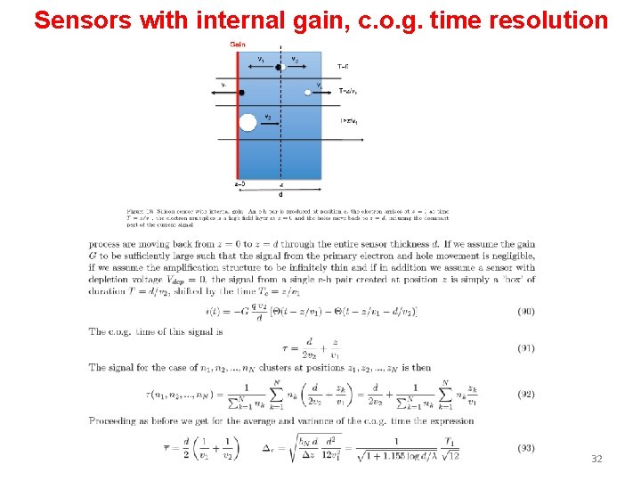
Sensors with internal gain, c. o. g. time resolution Werner Riegler, CERN 32

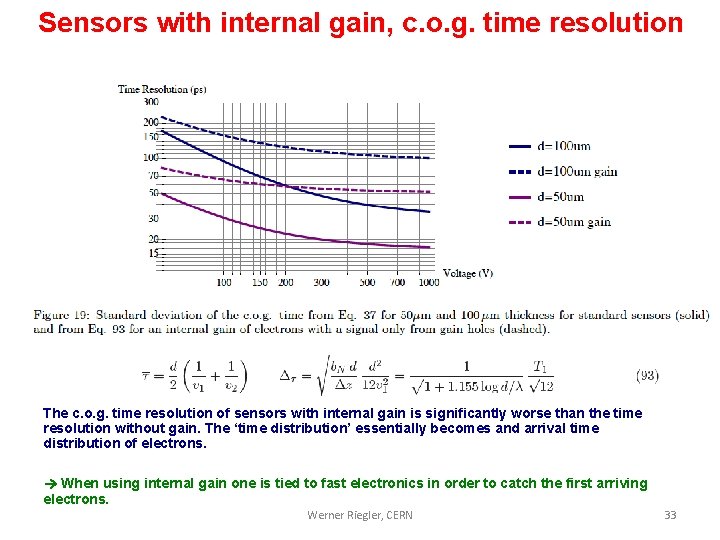
Sensors with internal gain, c. o. g. time resolution The c. o. g. time resolution of sensors with internal gain is significantly worse than the time resolution without gain. The ‘time distribution’ essentially becomes and arrival time distribution of electrons. When using internal gain one is tied to fast electronics in order to catch the first arriving electrons. Werner Riegler, CERN 33

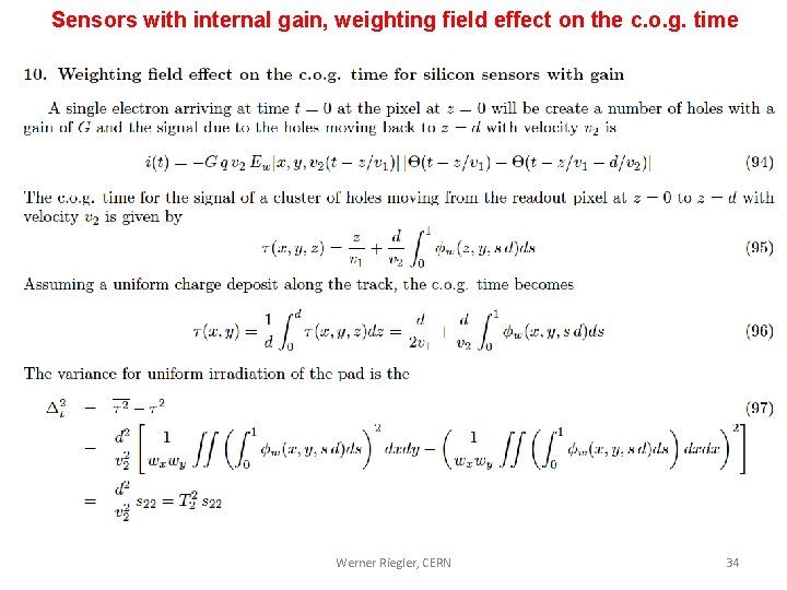
Sensors with internal gain, weighting field effect on the c. o. g. time Werner Riegler, CERN 34

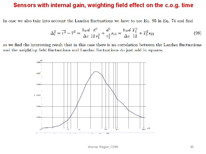
Sensors with internal gain, weighting field effect on the c. o. g. time Werner Riegler, CERN 35

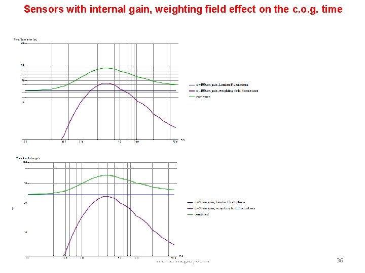
Sensors with internal gain, weighting field effect on the c. o. g. time Werner Riegler, CERN 36

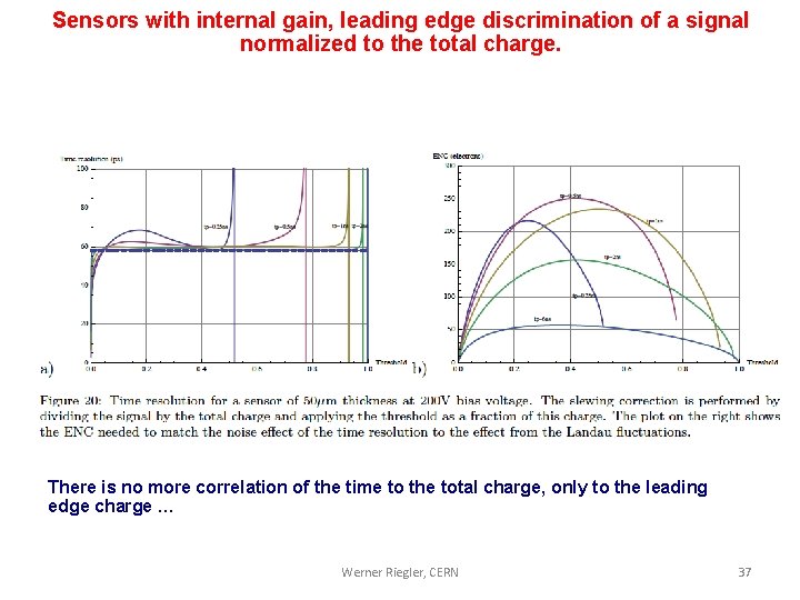
Sensors with internal gain, leading edge discrimination of a signal normalized to the total charge. There is no more correlation of the time to the total charge, only to the leading edge charge … Werner Riegler, CERN 37

Summary The c. o. g. time of a signal is measured by using an amplifier response time (peaking time) that is longer than the signal duration. It might represent an interesting way to measure timing with relatively ‘slow’ electronics – if noise allows. The ‘standard deviation’ of the center of gravity (c. o. g. ) time of a silicon sensor signal of 50/200 um thickness due to Landau fluctuations is 23/180 ps at 200 V, assuming large pads and negligible depletion voltage. To minimize the weighting field effect on the c. o. g. time resolution, the electrons should move towards the pad while the holes move away from the pad. For a 50 um sensor with 50 x 50 um pixels, the weighting field effect should still not destroy the time resolution. N. B. – the formulas hold for perpendicular tracks neglecting diffusion ! Using internal gain, one is tied to fast electronics and leading edge discrimination to catch the first arriving electrons. The slewing (from pulseheight variations) in sensors with gain is not related to the total charge but to the ‘leading edge charge’ i. e. constant fraction techniques using the leading edge. Werner Riegler, CERN 38