A 30 GSsec Track and Hold Amplifier in
![Circuit Comparison fsample [GS/s] Track BW [GHz] THD [d. B @ fin] Supply Power Circuit Comparison fsample [GS/s] Track BW [GHz] THD [d. B @ fin] Supply Power](https://slidetodoc.com/presentation_image_h/2b1e61bd945a09b8254b9fe9bdc3b373/image-32.jpg)
- Slides: 34

A 30 -GS/sec Track and Hold Amplifier in 0. 13 -µm CMOS Technology Shahriar Shahramian Sorin P. Voinigescu Anthony Chan Carusone Department of Electrical & Computer Eng. University of Toronto Canada

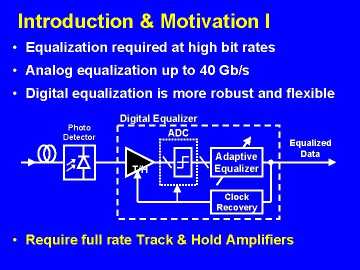
Introduction & Motivation I • Equalization required at high bit rates • Analog equalization up to 40 Gb/s • Digital equalization is more robust and flexible Photo Detector Digital Equalizer ADC T/H Adaptive Equalizer Equalized Data Clock Recovery • Require full rate Track & Hold Amplifiers

Introduction & Motivation II • Demonstrated 40 -GS/sec THA in Si. Ge Bi. CMOS – f. T and f. MAX of 160 GHz • CMOS technologies scaling to nanometre – f. T and f. MAX exceed 200 GHz for in production CMOS • CMOS is a serious contender for implementing DSP based equalizers above 10 Gb/s

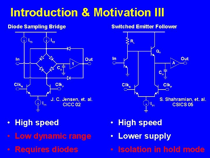
Introduction & Motivation III Diode Sampling Bridge J. C. Jensen, et. al. CICC 02 Switched Emitter Follower S. Shahramian, et. al. CSICS 05 • High speed • Low dynamic range • Lower supply • Requires diodes • Isolation in hold mode

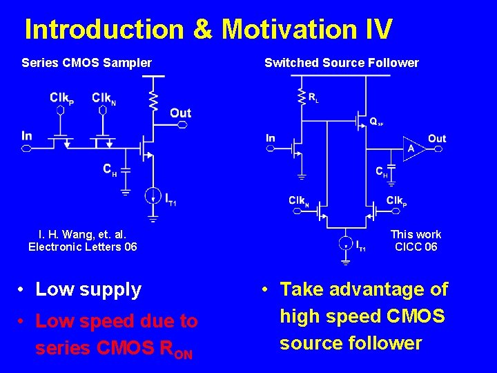
Introduction & Motivation IV Series CMOS Sampler I. H. Wang, et. al. Electronic Letters 06 • Low supply • Low speed due to series CMOS RON Switched Source Follower This work CICC 06 • Take advantage of high speed CMOS source follower

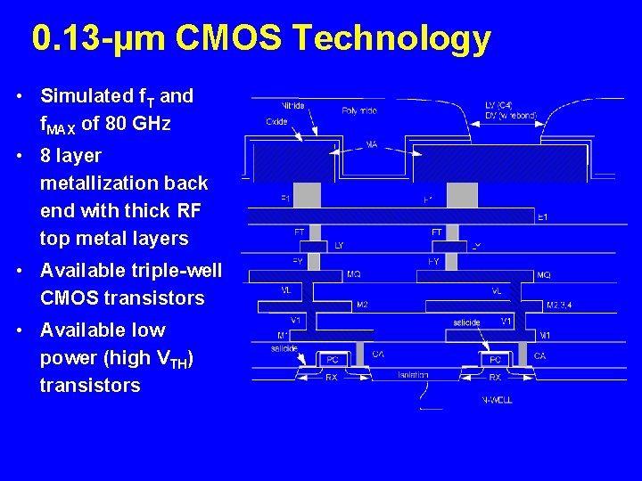
0. 13 -µm CMOS Technology • Simulated f. T and f. MAX of 80 GHz • 8 layer metallization back end with thick RF top metal layers • Available triple-well CMOS transistors • Available low power (high VTH) transistors

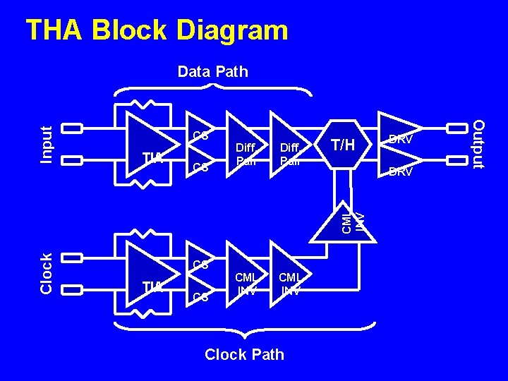
THA Block Diagram CS CS Diff. Pair CML INV T/H Clock CS TIA CS Clock Path DRV CML INV TIA Diff. Pair Output Input Data Path

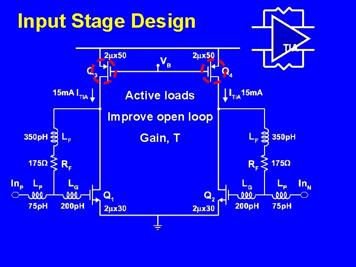
Input Stage Design TIA Active loads Improve open loop Gain, T

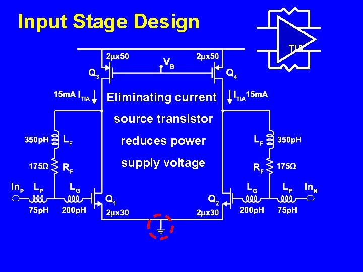
Input Stage Design TIA Eliminating current source transistor reduces power supply voltage

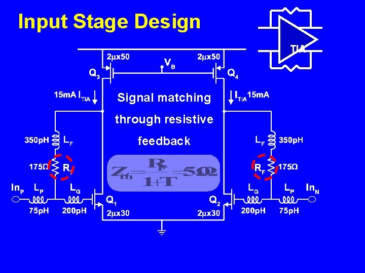
Input Stage Design TIA Signal matching through resistive feedback

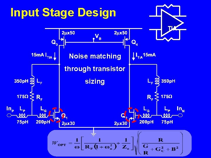
Input Stage Design TIA Noise matching through transistor sizing

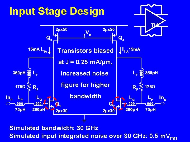
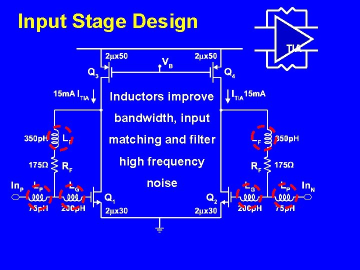
Input Stage Design TIA Transistors biased at J = 0. 25 m. A/µm, increased noise figure for higher bandwidth Simulated bandwidth: 30 GHz Simulated input integrated noise over 30 GHz: 0. 5 m. Vrms

Input Stage Design TIA Inductors improve bandwidth, input matching and filter high frequency noise

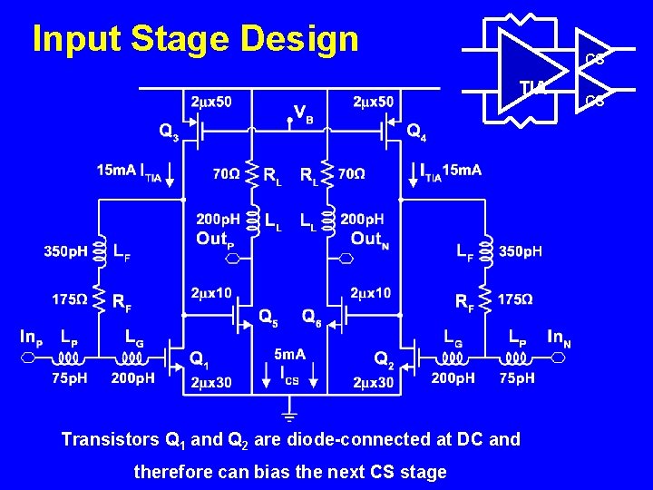
Input Stage Design CS TIA Transistors Q 1 and Q 2 are diode-connected at DC and therefore can bias the next CS stage CS

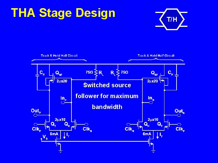
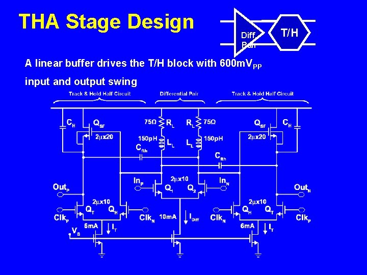
THA Stage Design Switched source follower for maximum bandwidth T/H

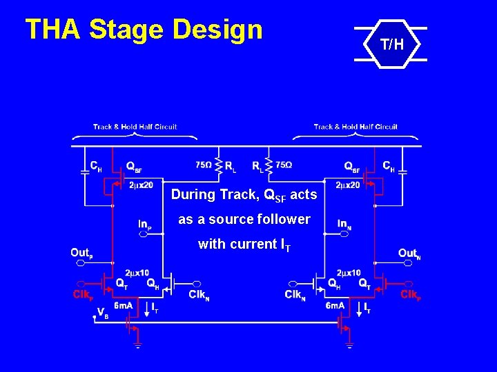
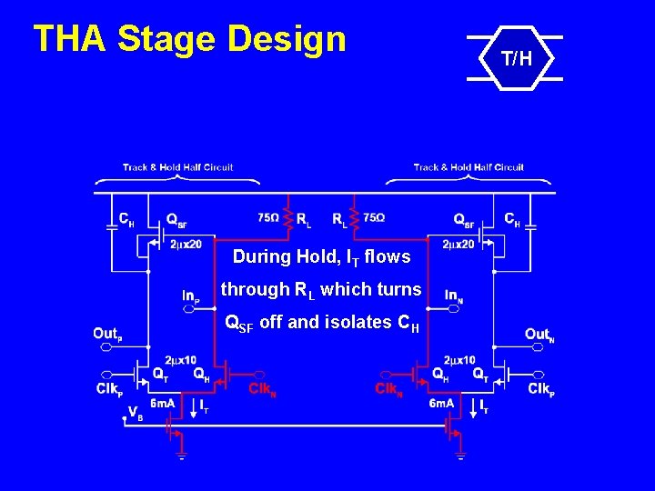
THA Stage Design During Track, QSF acts as a source follower with current IT T/H

THA Stage Design During Hold, IT flows through RL which turns QSF off and isolates CH T/H

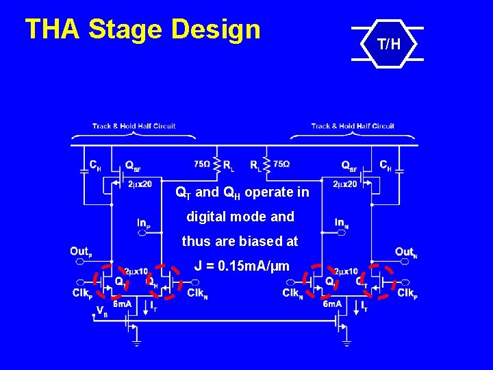
THA Stage Design QT and QH operate in digital mode and thus are biased at J = 0. 15 m. A/µm T/H

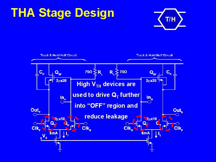
THA Stage Design High VTH devices are used to drive QT further into “OFF” region and reduce leakage T/H

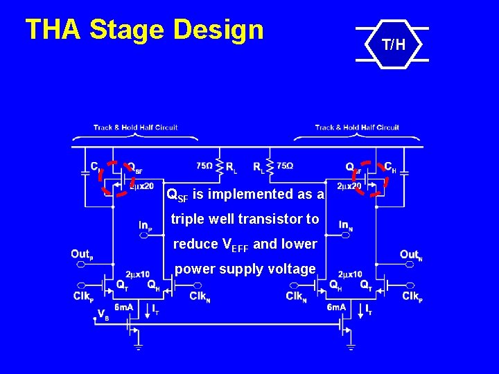
THA Stage Design QSF is implemented as a triple well transistor to reduce VEFF and lower power supply voltage T/H

THA Stage Design Diff. Pair A linear buffer drives the T/H block with 600 m. VPP input and output swing T/H

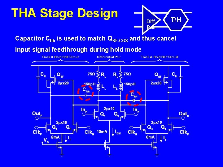
THA Stage Design Diff. Pair T/H Capacitor Cfth is used to match QSF-CGS and thus cancel input signal feedthrough during hold mode

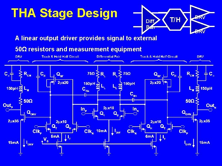
THA Stage Design Diff. Pair A linear output driver provides signal to external 50Ω resistors and measurement equipment T/H DRV

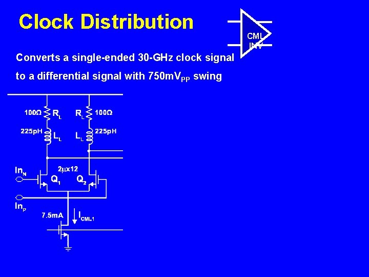
Clock Distribution Converts a single-ended 30 -GHz clock signal to a differential signal with 750 m. VPP swing CML INV

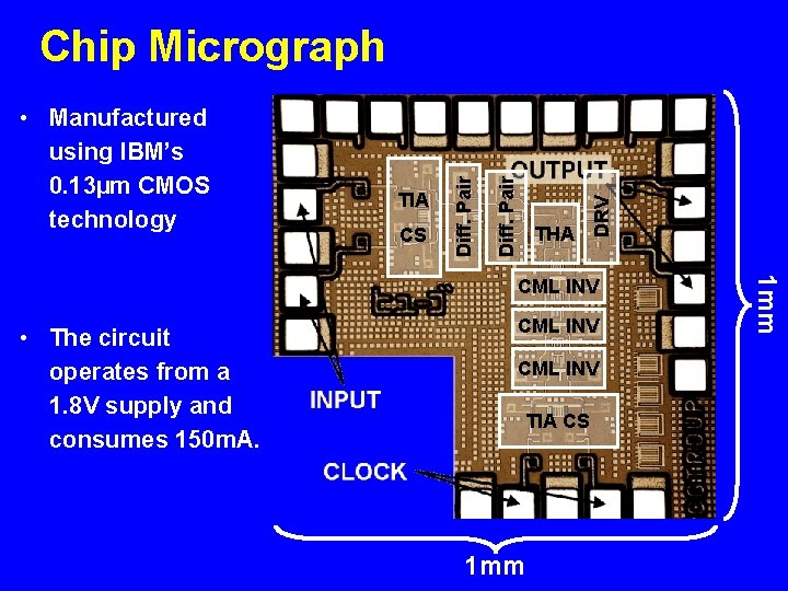
CS THA DRV TIA Diff. Pair • Manufactured using IBM’s 0. 13µm CMOS technology Diff. Pair Chip Micrograph • The circuit operates from a 1. 8 V supply and consumes 150 m. A. CML INV TIA CS 1 mm CML INV

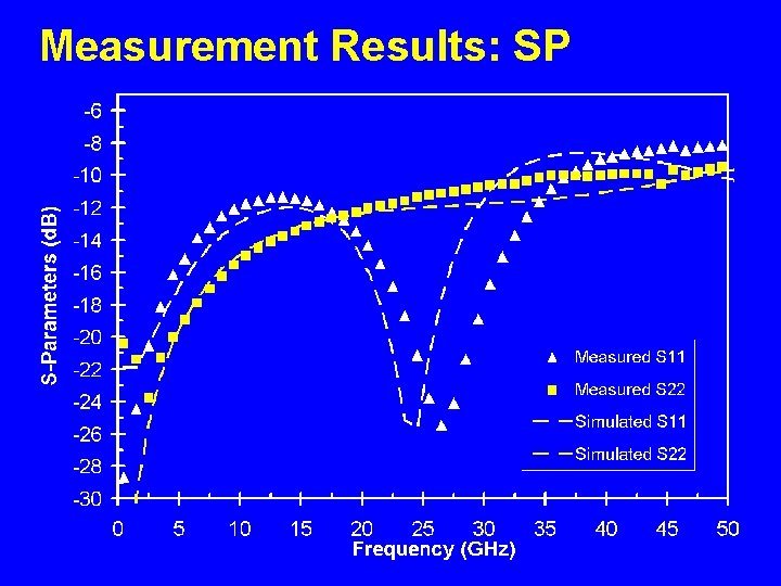
Measurement Results: SP

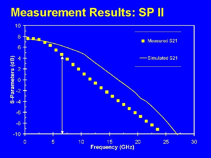
Measurement Results: SP II

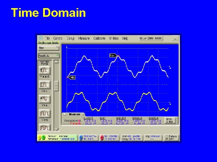
Time Domain

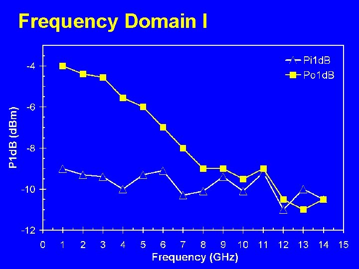
Frequency Domain I

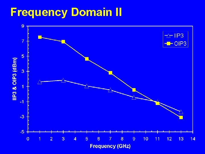
Frequency Domain II

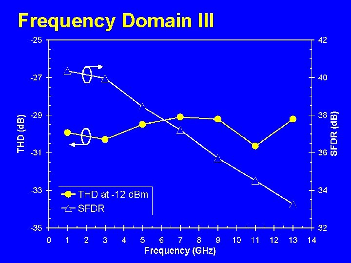
Frequency Domain III
![Circuit Comparison fsample GSs Track BW GHz THD d B fin Supply Power Circuit Comparison fsample [GS/s] Track BW [GHz] THD [d. B @ fin] Supply Power](https://slidetodoc.com/presentation_image_h/2b1e61bd945a09b8254b9fe9bdc3b373/image-32.jpg)
Circuit Comparison fsample [GS/s] Track BW [GHz] THD [d. B @ fin] Supply Power [V] [m. W] Process [N / f. T] This Work 30 7 -30 @ 1 GHz -29 @ 7 GHz 1. 8 270 CMOS 0. 13µm I. H. Wang el. al. Electronic Letters 06 10 N/A -24. 7 @ 5 GHz 1. 8 200 CMOS 0. 18µm J. Lee et. al. JSSC 03 12 14 -23. 3 @ 12 GHz -5. 2 390 In. P 120 GHz S. Shahramian et al. CSICS 05 40 43 -27 @ 20 GHz -29 @ 10 GHz 3. 6 540 Si. Ge 160 GHz Y. Lu et. al. BCTM 05 12 5. 5 -52. 4 @ 1. 5 GHz 3. 5 700 Si. Ge 200 GHz

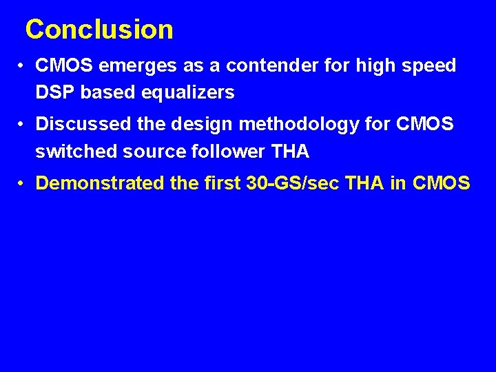
Conclusion • CMOS emerges as a contender for high speed DSP based equalizers • Discussed the design methodology for CMOS switched source follower THA • Demonstrated the first 30 -GS/sec THA in CMOS

Acknowledgement • CMC for chip fabrication and providing CAD tools • NSERC for financial support • OIT and CFI for equipment • ECIT for providing the network analyzer