WARP PROCESSORS ROMAN LYSECKY GREG STITT FRANK VAHID

- Slides: 27

WARP PROCESSORS ROMAN LYSECKY GREG STITT FRANK VAHID Presented by: Xin Guan Mar. 17, 2010

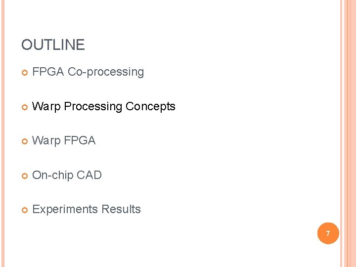
OUTLINE FPGA Co-processing Warp Processing Concepts Warp FPGA On-chip CAD Experiments Results 2

OUTLINE FPGA Co-processing Warp Processing Concepts Warp FPGA On-chip CAD Experiments Results 3

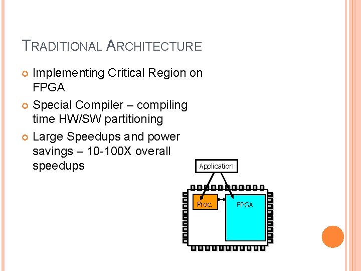
TRADITIONAL ARCHITECTURE Implementing Critical Region on FPGA Special Compiler – compiling time HW/SW partitioning Large Speedups and power savings – 10 -100 X overall Application speedups Proc. FPGA

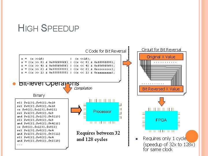
HIGH SPEEDUP Circuit for Bit Reversal C Code for Bit Reversal x x x l = = = (x ((x ((x >>16) >> 8) >> 4) >> 2) >> 1) & & 0 x 00 ff) 0 x 0 f 0 f) 0 x 3333) 0 x 5555) | | | (x ((x ((x <<16); << 8) & << 4) & << 2) & << 1) & X Value Bit. Original Reversed X Value. . . 0 xff 00); 0 xf 0 f 0); 0 xcccc); 0 xaaaa); Bit-level Operations . . . Compilation Bit Reversed XX Value Binary sll $v 1[3], $v 0[2], 0 x 10 srl $v 0[2], 0 x 10 or $v 0[2], $v 1[3], $v 0[2] srl $v 1[3], $v 0[2], 0 x 8 and $v 1[3], $t 5[13] sll $v 0[2], 0 x 8 and $v 0[2], $t 4[12] or $v 0[2], $v 1[3], $v 0[2] srl $v 1[3], $v 0[2], 0 x 4 and $v 1[3], $t 3[11] sll $v 0[2], 0 x 4 and $v 0[2], $t 2[10]. . . Requires between 32 and 128 cycles n Requires only 1 cycle (speedup of 32 x to 128 x) for same clock

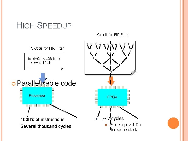
HIGH SPEEDUP Circuit for FIR Filter C Code for FIR Filter * * * + + + for (i=0; i < 128; i++) y += c[i] * x[i]. . + + + Parallelizable code 1000’s of instructions Several thousand cycles n ~ 7 cycles n Speedup > 100 x for same clock

OUTLINE FPGA Co-processing Warp Processing Concepts Warp FPGA On-chip CAD Experiments Results 7

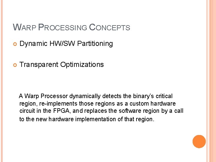
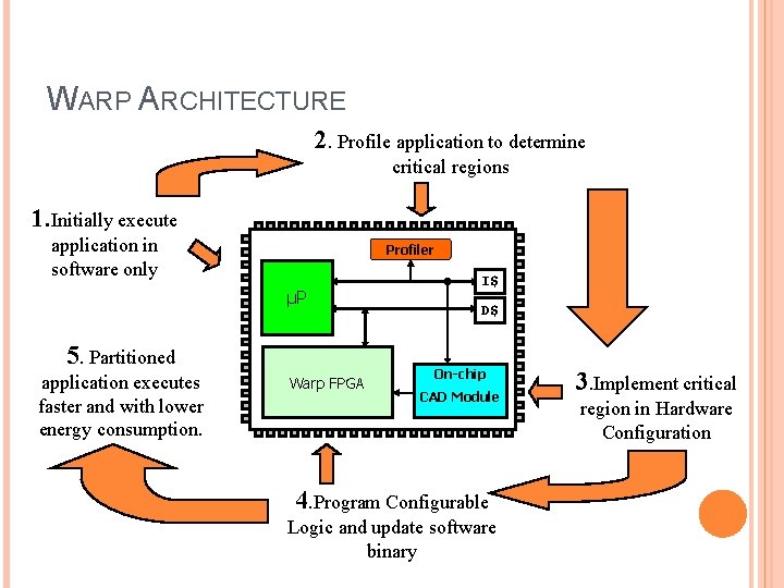
WARP PROCESSING CONCEPTS Dynamic HW/SW Partitioning Transparent Optimizations A Warp Processor dynamically detects the binary’s critical region, re-implements those regions as a custom hardware circuit in the FPGA, and replaces the software region by a call to the new hardware implementation of that region.

WARP ARCHITECTURE 2. Profile application to determine critical regions 1. Initially execute application in software only Profiler µP 5. Partitioned application executes faster and with lower energy consumption. Warp FPGA I$ D$ On-chip CAD Module 4. Program Configurable Logic and update software binary 3. Implement critical region in Hardware Configuration

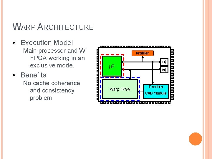
WARP ARCHITECTURE • Execution Model Main processor and WFPGA working in an exclusive mode. Profiler µP • Benefits No cache coherence and consistency problem Warp FPGA I$ D$ On-chip CAD Module

OUTLINE FPGA Co-processing Warp Processing Concepts Warp FPGA On-chip CAD Experiments Results 11

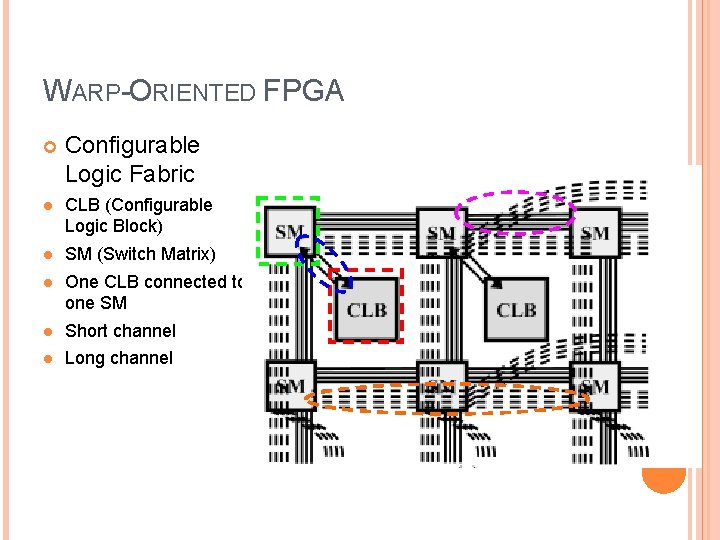
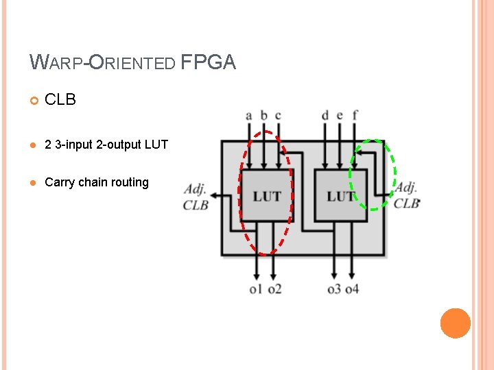
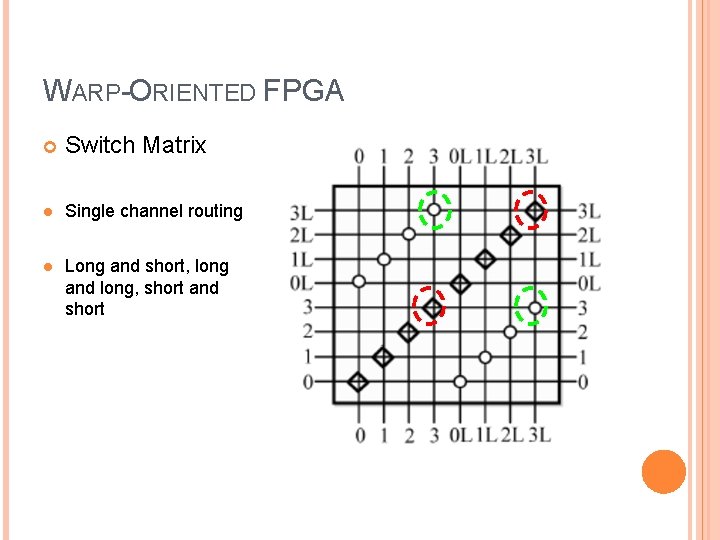
WARP-ORIENTED FPGA Configurable Logic Fabric l CLB (Configurable Logic Block) l SM (Switch Matrix) l One CLB connected to one SM l Short channel l Long channel

WARP-ORIENTED FPGA CLB l 2 3 -input 2 -output LUT l Carry chain routing

WARP-ORIENTED FPGA Switch Matrix l Single channel routing l Long and short, long and long, short and short

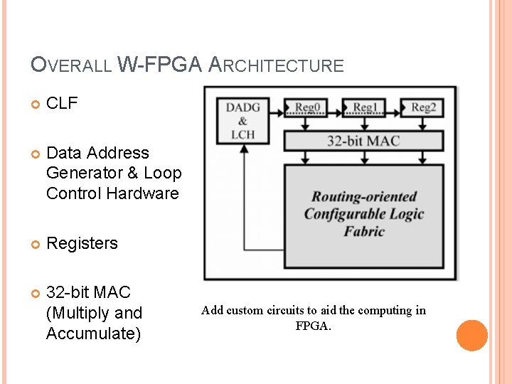
OVERALL W-FPGA ARCHITECTURE CLF Data Address Generator & Loop Control Hardware Registers 32 -bit MAC (Multiply and Accumulate) Add custom circuits to aid the computing in FPGA.

OUTLINE FPGA Co-processing Warp Processing Concepts Warp FPGA On-chip CAD Experiments Results 16

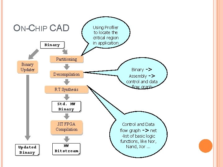
ON-CHIP CAD Binary Using Profiler to locate the critical region in application Partitioning Binary Updater Decompilation RT Synthesis -> Assembly -> Binary control and data flow graph Std. HW Binary JIT FPGA Compilation Updated Binary HW Binary Bitstream Control and Data flow graph -> net -list of basic logic functions, like Nor, Nand, Xor …

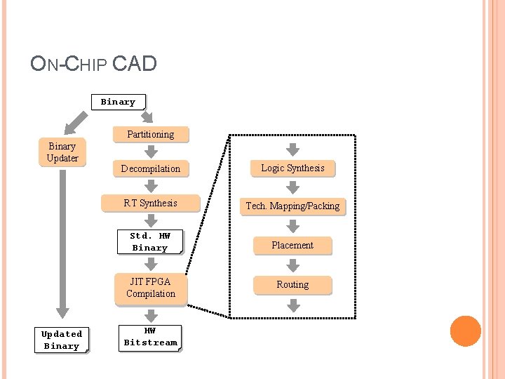
ON-CHIP CAD Binary Partitioning Binary Updater Updated Binary Decompilation Logic Synthesis RT Synthesis Tech. Mapping/Packing Std. HW Binary Placement JIT FPGA Compilation Routing HW Binary Bitstream

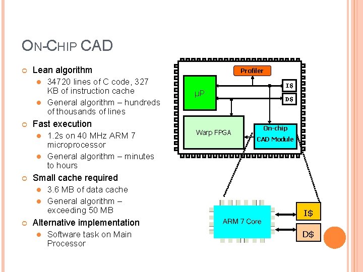
ON-CHIP CAD Lean algorithm 34720 lines of C code, 327 KB of instruction cache l General algorithm – hundreds of thousands of lines Profiler l Fast execution 1. 2 s on 40 MHz ARM 7 microprocessor l General algorithm – minutes to hours l µP Warp FPGA I$ D$ On-chip CAD Module Small cache required 3. 6 MB of data cache l General algorithm – exceeding 50 MB l Alternative implementation l Software task on Main Processor I$ D$

OUTLINE FPGA Co-processing Warp Processing Concepts Warp FPGA On-chip CAD Experiments Results 20

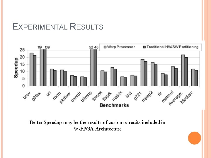
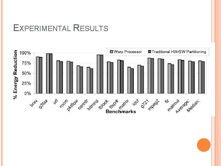
EXPERIMENTAL RESULTS Comparing Warp Processor Implementation and Traditional HW/SW Partition Implementation (Special Complier, and Xilinx FPGA) on embedded benchmarks. Speedups for the same critical region chosen by Profiler in Warp Processor Energy Consumption for the same critical region chosen by Profiler in Warp Processor

EXPERIMENTAL RESULTS Better Speedup may be the results of custom circuits included in W-FPGA Architecture

EXPERIMENTAL RESULTS

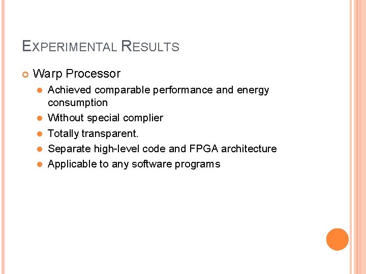
EXPERIMENTAL RESULTS Warp Processor l l l Achieved comparable performance and energy consumption Without special complier Totally transparent. Separate high-level code and FPGA architecture Applicable to any software programs

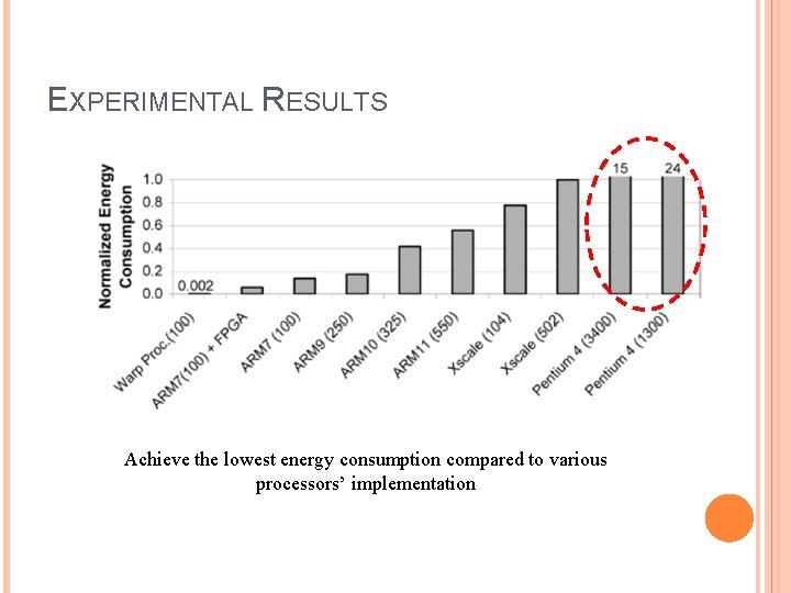
EXPERIMENTAL RESULTS Achieve the lowest energy consumption compared to various processors’ implementation

CONCLUSION Feasibility Improved lean algorithm for partitioning, synthesis, placement and routing Improved Warp FPGA architecture

Questions ?