SingleCycle CPU Datapath Control 1 Review Processor Design
![Summary of the Control Signals (1/2) inst Register Transfer add R[rd] R[rs] + R[rt]; Summary of the Control Signals (1/2) inst Register Transfer add R[rd] R[rs] + R[rt];](https://slidetodoc.com/presentation_image_h/f7d3ecc5a8225c215187fd3d949f9321/image-8.jpg)

- Slides: 34

Single-Cycle CPU Datapath Control 1

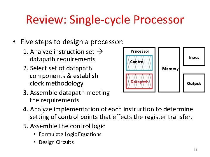
Review: Processor Design 5 steps Step 1: Analyze instruction set to determine datapath requirements – Meaning of each instruction is given by register transfers – Datapath must include storage element for ISA registers – Datapath must support each register transfer Step 2: Select set of datapath components & establish clock methodology Step 3: Assemble datapath components that meet the requirements Step 4: Analyze implementation of each instruction to determine setting of control points that realizes the register transfer Step 5: Assemble the control logic 2

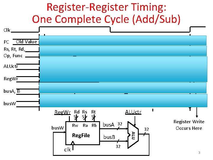
Register-Register Timing: One Complete Cycle (Add/Sub) Clk PC Old Value Rs, Rt, Rd, Op, Func Old Value ALUctr Old Value Reg. Wr Old Value bus. A, B Old Value bus. W Old Value New Value Instruction Memory Access Time New Value Delay through Control Logic New Value Register File Access Time New Value ALU Delay New Value ALUctr Reg. Wr Rd Rs Rt 5 bus. W 5 Rw Ra Rb bus. A Reg. File bus. B 32 ALU clk 5 32 Register Write Occurs Here 32 3

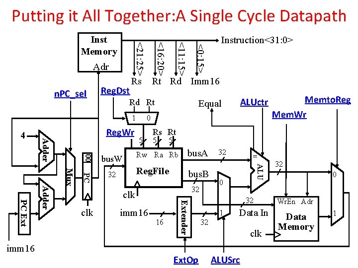
Putting it All Together: A Single Cycle Datapath Reg. Dst 00 32 0 5 5 5 Rw Ra Rb Reg. File bus. A bus. B 32 16 Extender imm 16 Memto. Reg Mem. Wr Rs Rt clk ALUctr Equal Ext. Op 32 = ALU bus. W PC Mux Adder PC Ext imm 16 Reg. Wr Adder 4 Rt Rd Imm 16 Rd Rt 1 Instruction<31: 0> <0: 15> n. PC_sel Rs <11: 15> Adr <16: 20> <21: 25> Inst Memory 0 32 1 32 Data In clk ALUSrc 32 0 Wr. En Adr Data Memory 1

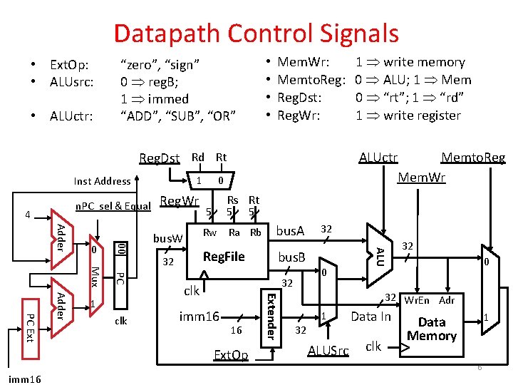
Datapath Control Signals • Ext. Op: • ALUsrc: • ALUctr: • • “zero”, “sign” 0 reg. B; 1 immed “ADD”, “SUB”, “OR” Mem. Wr: Memto. Reg: Reg. Dst: Reg. Wr: ALUctr Memto. Reg Mem. Wr Reg. Dst Rd Rt 1 Inst Address 4 PC Mux clk bus. W 32 Rs Rt 5 5 Rw Ra Rb bus. A Reg. File bus. B 32 clk imm 16 16 Ext. Op imm 16 5 Extender PC Ext Adder 1 Reg. Wr 0 32 0 ALU Adder 0 00 n. PC_sel & Equal 1 write memory 0 ALU; 1 Mem 0 “rt”; 1 “rd” 1 write register 32 0 32 Wr. En Adr 32 1 ALUSrc Data In clk 1 Data Memory 6

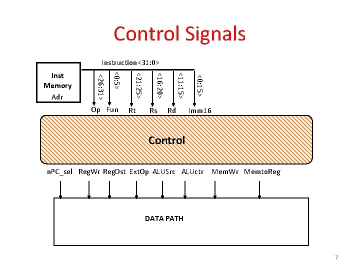
Control Signals Instruction<31: 0> Rd <0: 15> Rs <11: 15> Rt <16: 20> Op Fun <21: 25> <0: 5> <26: 31> Inst Memory Adr Imm 16 Control n. PC_sel Reg. Wr Reg. Dst Ext. Op ALUSrc ALUctr Mem. Wr Memto. Reg DATA PATH 7

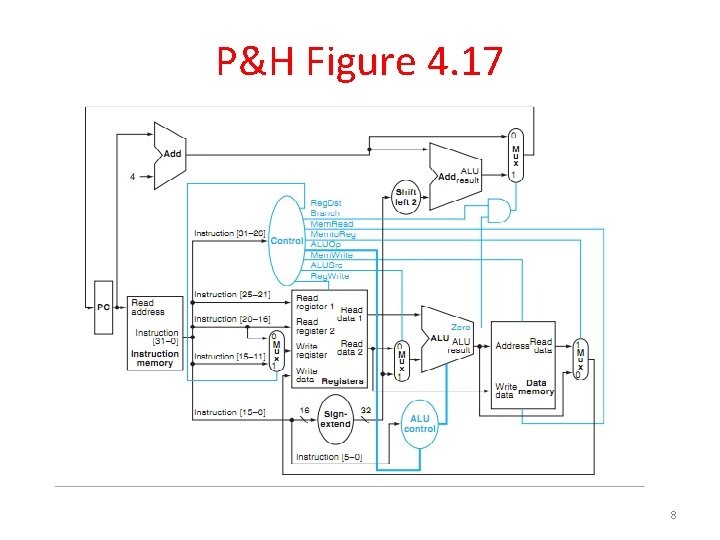
P&H Figure 4. 17 8
![Summary of the Control Signals 12 inst Register Transfer add Rrd Rrs Rrt Summary of the Control Signals (1/2) inst Register Transfer add R[rd] R[rs] + R[rt];](https://slidetodoc.com/presentation_image_h/f7d3ecc5a8225c215187fd3d949f9321/image-8.jpg)
Summary of the Control Signals (1/2) inst Register Transfer add R[rd] R[rs] + R[rt]; PC + 4 ALUsrc=Reg. B, ALUctr=“ADD”, Reg. Dst=rd, Reg. Wr, n. PC_sel=“+4” sub R[rd] R[rs] – R[rt]; PC + 4 ALUsrc=Reg. B, ALUctr=“SUB”, Reg. Dst=rd, Reg. Wr, n. PC_sel=“+4” ori R[rt] R[rs] + zero_ext(Imm 16); PC + 4 ALUsrc=Im, Extop=“Z”, ALUctr=“OR”, Reg. Dst=rt, Reg. Wr, n. PC_sel=“+4” lw R[rt] MEM[ R[rs] + sign_ext(Imm 16)]; PC + 4 ALUsrc=Im, Extop=“sn”, ALUctr=“ADD”, Memto. Reg, Reg. Dst=rt, Reg. Wr, sw n. PC_sel = “+ MEM[ R[rs] + sign_ext(Imm 16)] R[rs]; PC + 4 ALUsrc=Im, Extop=“sn”, ALUctr = “ADD”, Mem. Wr, n. PC_sel = “+4” beq if (R[rs] == R[rt]) then PC + sign_ext(Imm 16)] || 00 else PC + 4 n. PC_sel = “br”, ALUctr = “SUB” 9

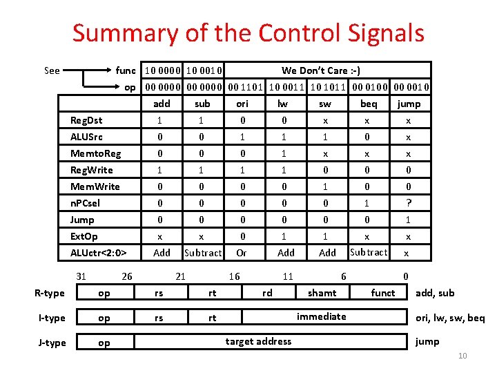
Summary of the Control Signals See func 10 0000 10 0010 We Don’t Care : -) op 00 0000 00 1101 10 0011 10 1011 00 0100 00 0010 Reg. Dst ALUSrc Memto. Reg. Write Mem. Write add 1 0 0 1 0 sub 1 0 0 1 0 ori 0 1 0 lw 0 1 1 1 0 sw x 1 x 0 1 beq x 0 0 jump x x x 0 0 n. PCsel Jump Ext. Op ALUctr<2: 0> 0 0 x Add 0 0 x Subtract 0 0 0 Or 0 0 1 Add 1 0 x Subtract ? 1 x x 31 26 21 16 R-type op rs rt I-type op rs rt J-type op 11 rd 6 shamt immediate target address 0 funct add, sub ori, lw, sw, beq jump 10

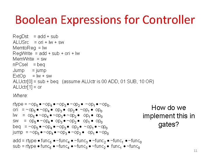
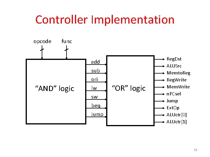
Boolean Expressions for Controller Reg. Dst = add + sub ALUSrc = ori + lw + sw Memto. Reg = lw Reg. Write = add + sub + ori + lw Mem. Write = sw n. PCsel = beq Jump = jump Ext. Op = lw + sw ALUctr[0] = sub + beq (assume ALUctr is 00 ADD, 01 SUB, 10 OR) ALUctr[1] = or Where: rtype = ~op 5 ~op 4 ~op 3 ~op 2 ~op 1 ~op 0, ori = ~op 5 ~op 4 op 3 op 2 ~op 1 op 0 lw = op 5 ~op 4 ~op 3 ~op 2 op 1 op 0 sw = op 5 ~op 4 op 3 ~op 2 op 1 op 0 beq = ~op 5 ~op 4 ~op 3 op 2 ~op 1 ~op 0 jump = ~op 5 ~op 4 ~op 3 ~op 2 op 1 ~op 0 add = rtype func 5 ~func 4 ~func 3 ~func 2 ~func 1 ~func 0 sub = rtype func 5 ~func 4 ~func 3 ~func 2 func 1 ~func 0 How do we implement this in gates? 11

Controller Implementation opcode func “AND” logic add sub ori lw sw beq jump “OR” logic Reg. Dst ALUSrc Memto. Reg. Write Mem. Write n. PCsel Jump Ext. Op ALUctr[0] ALUctr[1] 12

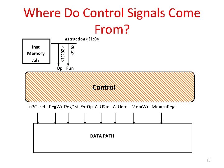
Where Do Control Signals Come From? Instruction<31: 0> Rd <0: 15> Rs <11: 15> Rt <16: 20> Op Fun <21: 25> <0: 5> <26: 31> Inst Memory Adr Imm 16 Control n. PC_sel Reg. Wr Reg. Dst Ext. Op ALUSrc ALUctr Mem. Wr Memto. Reg DATA PATH 13

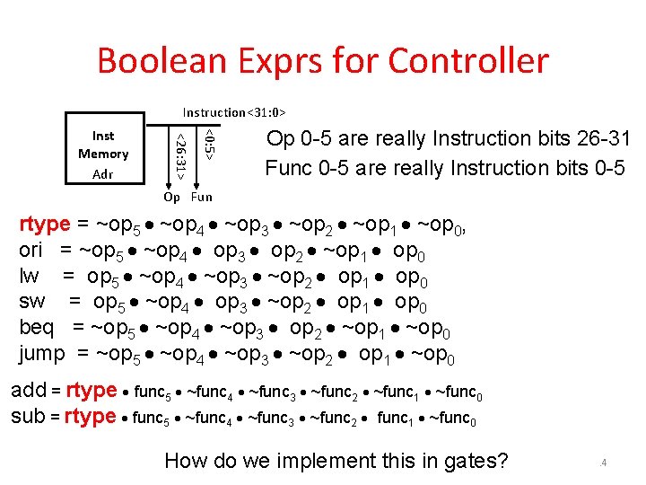
Boolean Exprs for Controller Instruction<31: 0> Rd <0: 15> Rs <11: 15> Rt Op 0 -5 are really Instruction bits 26 -31 Func 0 -5 are really Instruction bits 0 -5 <16: 20> Op Fun <21: 25> <0: 5> <26: 31> Inst Memory Adr Imm 16 rtype = ~op 5 ~op 4 ~op 3 ~op 2 ~op 1 ~op 0, ori = ~op 5 ~op 4 op 3 op 2 ~op 1 op 0 lw = op 5 ~op 4 ~op 3 ~op 2 op 1 op 0 sw = op 5 ~op 4 op 3 ~op 2 op 1 op 0 beq = ~op 5 ~op 4 ~op 3 op 2 ~op 1 ~op 0 jump = ~op 5 ~op 4 ~op 3 ~op 2 op 1 ~op 0 add = rtype func 5 ~func 4 ~func 3 ~func 2 ~func 1 ~func 0 sub = rtype func 5 ~func 4 ~func 3 ~func 2 func 1 ~func 0 How do. Fallwe implement this in gates? 2011 -- Lecture #30 14

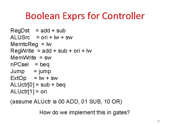
Boolean Exprs for Controller Reg. Dst = add + sub ALUSrc = ori + lw + sw Memto. Reg = lw Reg. Write = add + sub + ori + lw Mem. Write = sw n. PCsel = beq Jump = jump Ext. Op = lw + sw ALUctr[0] = sub + beq ALUctr[1] = ori (assume ALUctr is 00 ADD, 01 SUB, 10 OR) How do we implement this in gates? 15

Controller Implementation opcode func “AND” logic add sub ori lw sw beq jump “OR” logic Reg. Dst ALUSrc Memto. Reg. Write Mem. Write n. PCsel Jump Ext. Op ALUctr[0] ALUctr[1] 16

Review: Single-cycle Processor • Five steps to design a processor: Processor 1. Analyze instruction set Input datapath requirements Control Memory 2. Select set of datapath components & establish Datapath Output clock methodology 3. Assemble datapath meeting the requirements 4. Analyze implementation of each instruction to determine setting of control points that effects the register transfer. 5. Assemble the control logic • Formulate Logic Equations • Design Circuits 17

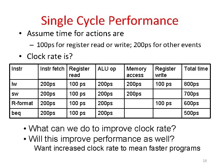
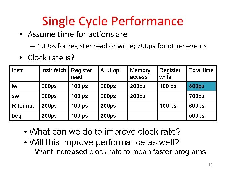
Single Cycle Performance • Assume time for actions are – 100 ps for register read or write; 200 ps for other events • Clock rate is? Instr fetch Register read ALU op Memory access Register write Total time lw 200 ps 100 ps 800 ps sw 200 ps 100 ps 200 ps R-format 200 ps 100 ps 200 ps beq 200 ps 100 ps 200 ps 700 ps 100 ps 600 ps 500 ps • What can we do to improve clock rate? • Will this improve performance as well? Want increased clock rate to mean faster programs 18

Single Cycle Performance • Assume time for actions are – 100 ps for register read or write; 200 ps for other events • Clock rate is? Instr fetch Register read ALU op Memory access Register write Total time lw 200 ps 100 ps 800 ps sw 200 ps 100 ps 200 ps R-format 200 ps 100 ps 200 ps beq 200 ps 100 ps 200 ps 700 ps 100 ps 600 ps 500 ps • What can we do to improve clock rate? • Will this improve performance as well? Want increased clock rate to mean faster programs 19

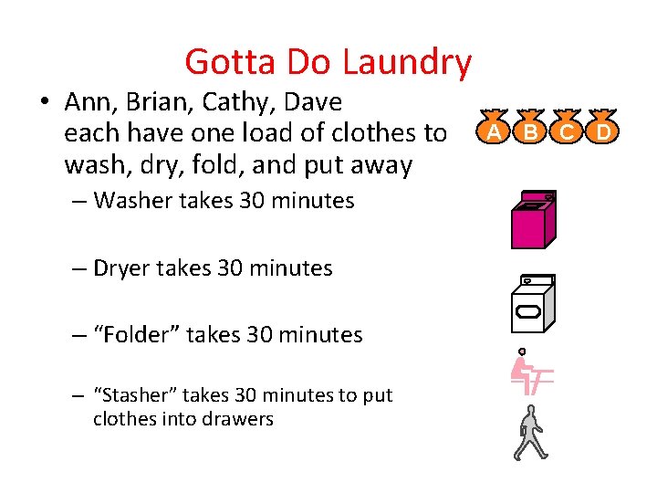
Gotta Do Laundry • Ann, Brian, Cathy, Dave each have one load of clothes to wash, dry, fold, and put away – Washer takes 30 minutes – Dryer takes 30 minutes – “Folder” takes 30 minutes – “Stasher” takes 30 minutes to put clothes into drawers A B C D

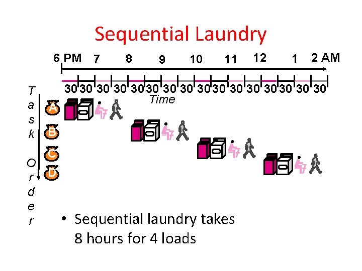
Sequential Laundry 6 PM 7 T a s k O r d e r A 8 9 10 11 12 1 2 AM 30 30 30 30 Time B C D • Sequential laundry takes 8 hours for 4 loads

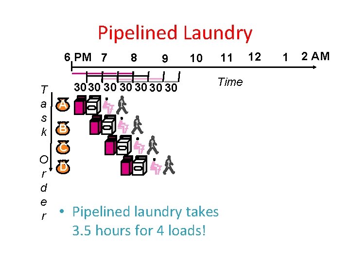
Pipelined Laundry 6 PM 7 T a s k 8 9 3030 30 30 11 10 Time A B C O D r d e r • Pipelined laundry takes 3. 5 hours for 4 loads! 12 1 2 AM

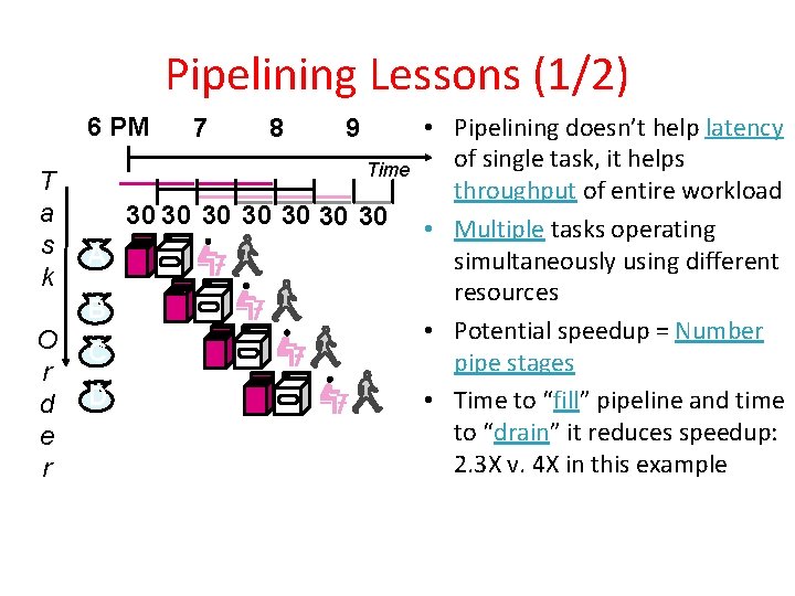
Pipelining Lessons (1/2) 6 PM T a s k 8 9 Time 30 30 A B O r d e r 7 C D • Pipelining doesn’t help latency of single task, it helps throughput of entire workload • Multiple tasks operating simultaneously using different resources • Potential speedup = Number pipe stages • Time to “fill” pipeline and time to “drain” it reduces speedup: 2. 3 X v. 4 X in this example

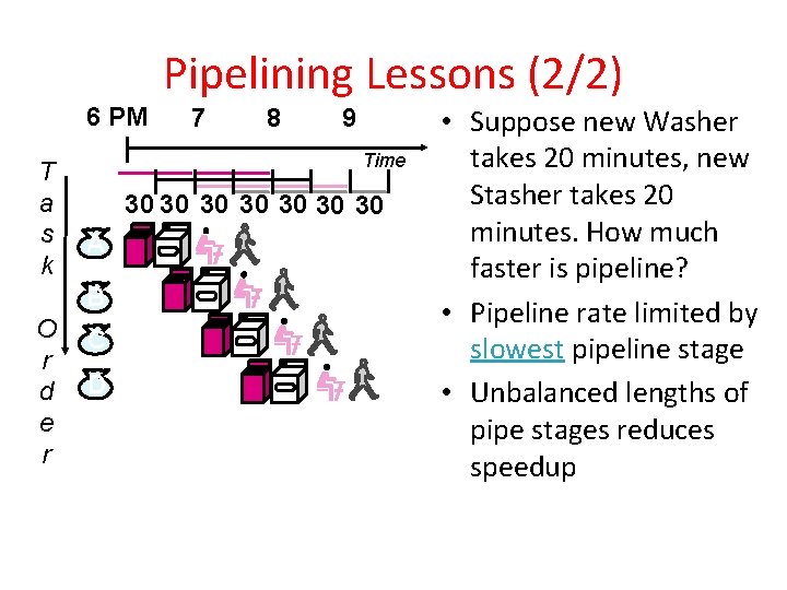
Pipelining Lessons (2/2) 6 PM T a s k 8 9 Time 30 30 A B O r d e r 7 C D • Suppose new Washer takes 20 minutes, new Stasher takes 20 minutes. How much faster is pipeline? • Pipeline rate limited by slowest pipeline stage • Unbalanced lengths of pipe stages reduces speedup

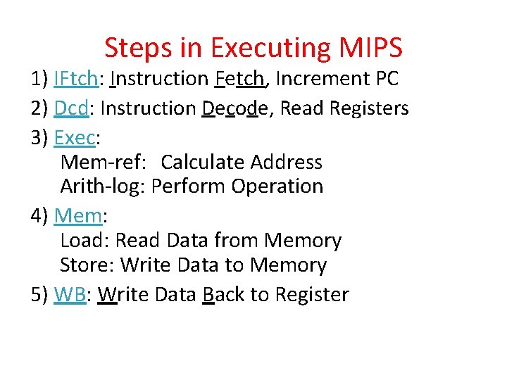
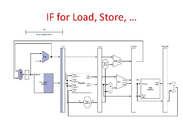
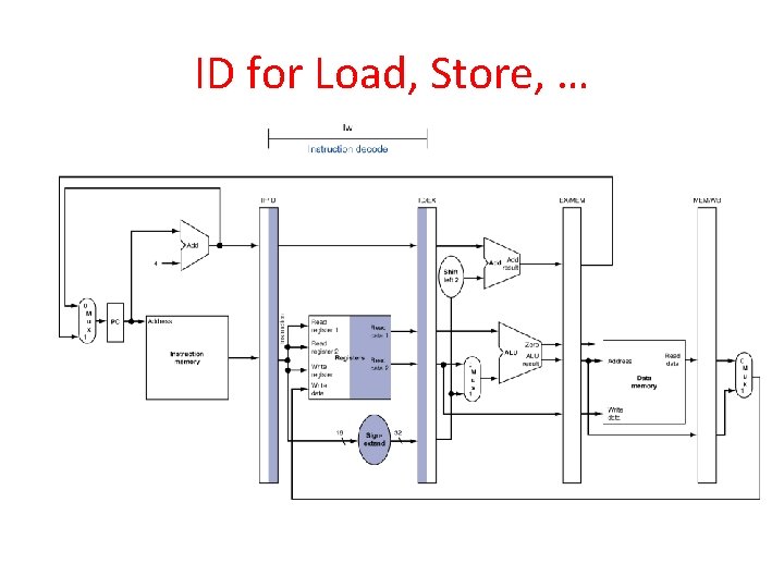
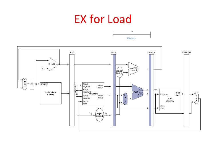
Steps in Executing MIPS 1) IFtch: Instruction Fetch, Increment PC 2) Dcd: Instruction Decode, Read Registers 3) Exec: Mem-ref: Calculate Address Arith-log: Perform Operation 4) Mem: Load: Read Data from Memory Store: Write Data to Memory 5) WB: Write Data Back to Register

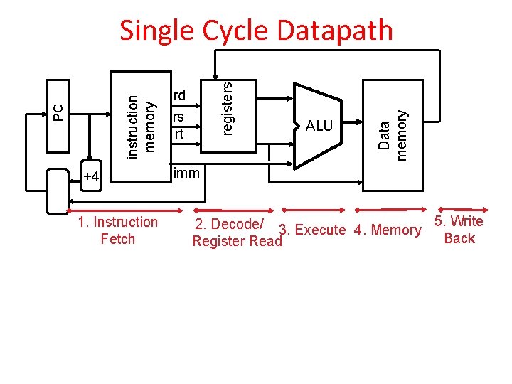
+4 1. Instruction Fetch rd rs rt ALU Data memory registers PC instruction memory Single Cycle Datapath imm 2. Decode/ 3. Execute 4. Memory 5. Write Back Register Read

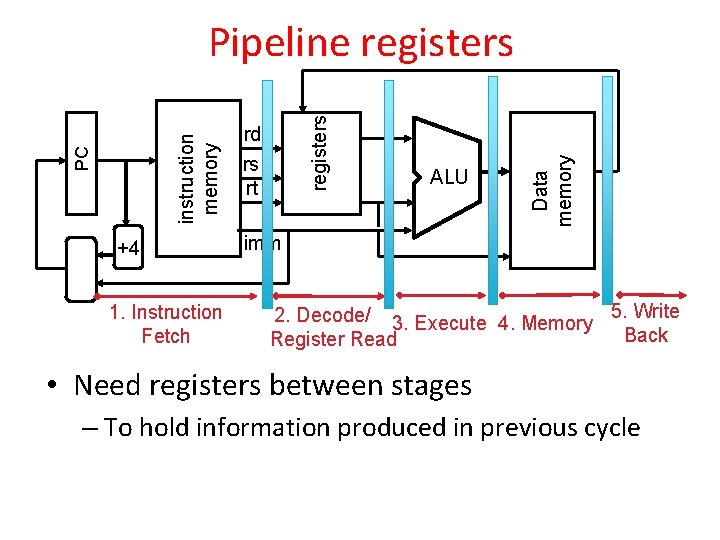
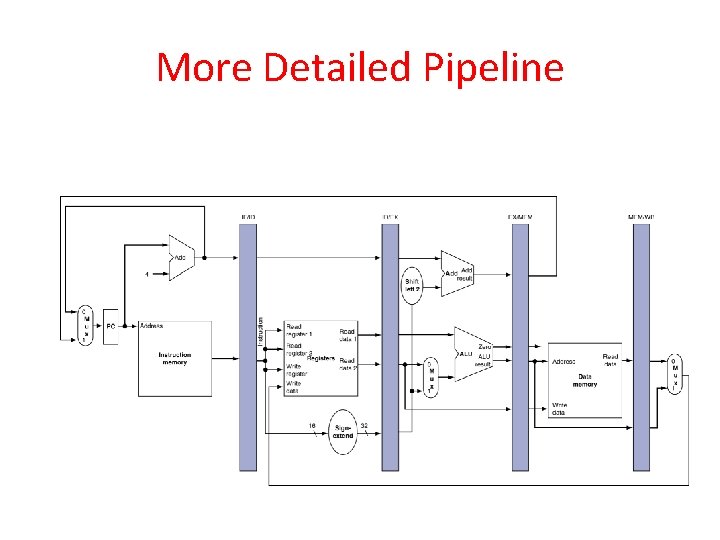
+4 1. Instruction Fetch rd rs rt ALU Data memory registers PC instruction memory Pipeline registers imm 2. Decode/ 3. Execute 4. Memory 5. Write Back Register Read • Need registers between stages – To hold information produced in previous cycle

More Detailed Pipeline

IF for Load, Store, …

ID for Load, Store, …

EX for Load

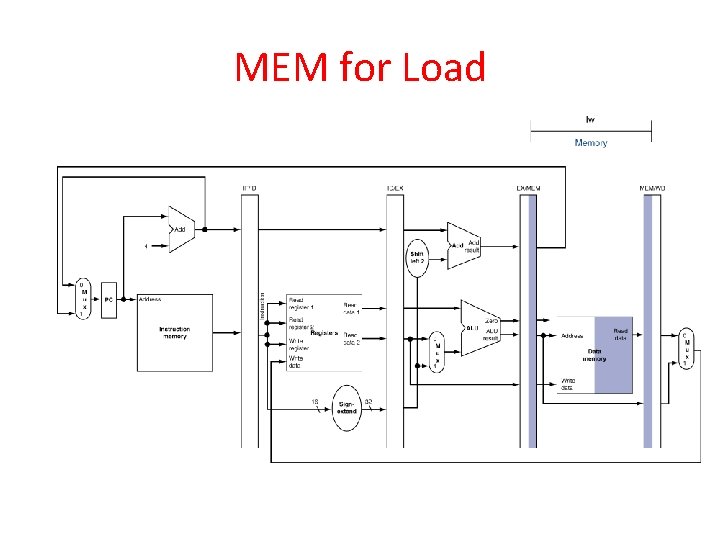
MEM for Load

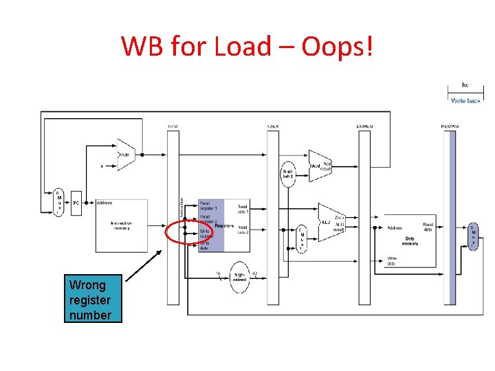
WB for Load – Oops! Wrong register number

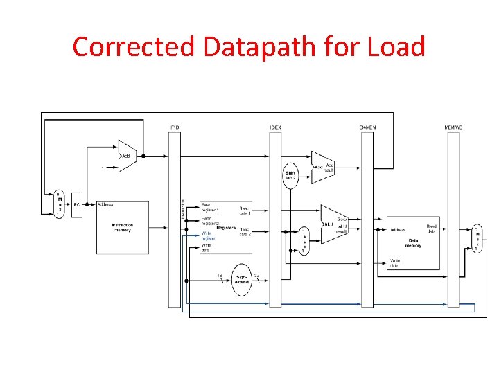
Corrected Datapath for Load

So, in conclusion • You now know how to implement the control logic for the single-cycle CPU. – (actually, you already knew it!) • Pipelining improves performance by increasing instruction throughput: exploits ILP – Executes multiple instructions in parallel – Each instruction has the same latency • Next: hazards in pipelining: – Structure, data, control 35