Semiconductor Device Physics Lecture 2 Dr Ing Erwin
- Slides: 33

Semiconductor Device Physics Lecture 2 Dr. -Ing. Erwin Sitompul President University http: //zitompul. wordpress. com President University Erwin Sitompul SDP 2/1

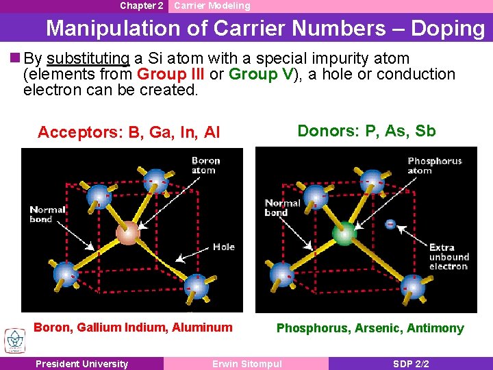
Chapter 2 Carrier Modeling Manipulation of Carrier Numbers – Doping n By substituting a Si atom with a special impurity atom (elements from Group III or Group V), a hole or conduction electron can be created. Donors: P, As, Sb Acceptors: B, Ga, In, Al Boron, Gallium Indium, Aluminum President University Phosphorus, Arsenic, Antimony Erwin Sitompul SDP 2/2

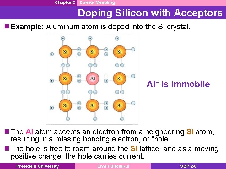
Chapter 2 Carrier Modeling Doping Silicon with Acceptors n Example: Aluminum atom is doped into the Si crystal. Al– is immobile n The Al atom accepts an electron from a neighboring Si atom, resulting in a missing bonding electron, or “hole”. n The hole is free to roam around the Si lattice, and as a moving positive charge, the hole carries current. President University Erwin Sitompul SDP 2/3

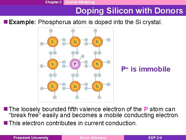
Chapter 2 Carrier Modeling Doping Silicon with Donors n Example: Phosphorus atom is doped into the Si crystal. P+ is immobile n The loosely bounded fifth valence electron of the P atom can “break free” easily and becomes a mobile conducting electron. n This electron contributes in current conduction. President University Erwin Sitompul SDP 2/4

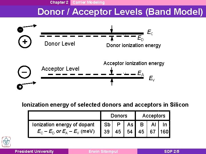
Chapter 2 Carrier Modeling Donor / Acceptor Levels (Band Model) ▬ + ▬ ED Donor Level Ec Donor ionization energy Acceptor Level EA Ev + Ionization energy of selected donors and acceptors in Silicon Donors Ionization energy of dopant EC – ED or EA – EV (me. V) President University Sb P 39 45 Erwin Sitompul Acceptors As B 54 45 Al In 67 160 SDP 2/5

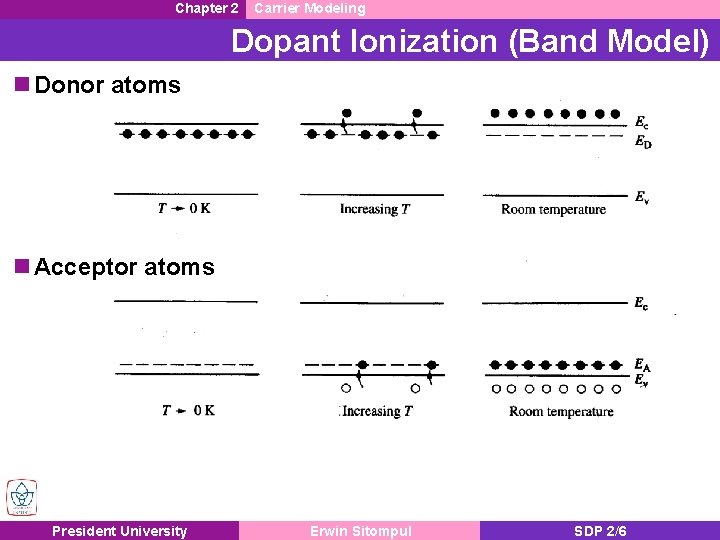
Chapter 2 Carrier Modeling Dopant Ionization (Band Model) n Donor atoms n Acceptor atoms President University Erwin Sitompul SDP 2/6

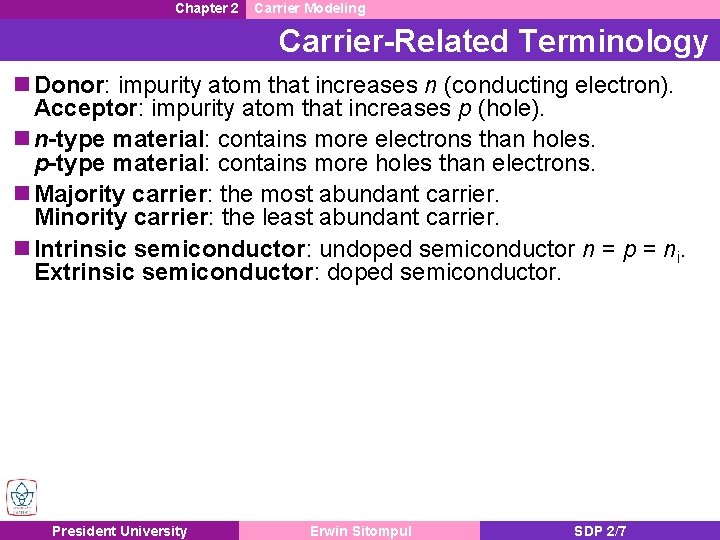
Chapter 2 Carrier Modeling Carrier-Related Terminology n Donor: impurity atom that increases n (conducting electron). Acceptor: impurity atom that increases p (hole). n n-type material: contains more electrons than holes. p-type material: contains more holes than electrons. n Majority carrier: the most abundant carrier. Minority carrier: the least abundant carrier. n Intrinsic semiconductor: undoped semiconductor n = p = ni. Extrinsic semiconductor: doped semiconductor. President University Erwin Sitompul SDP 2/7

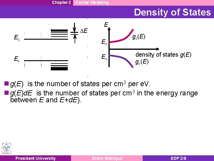
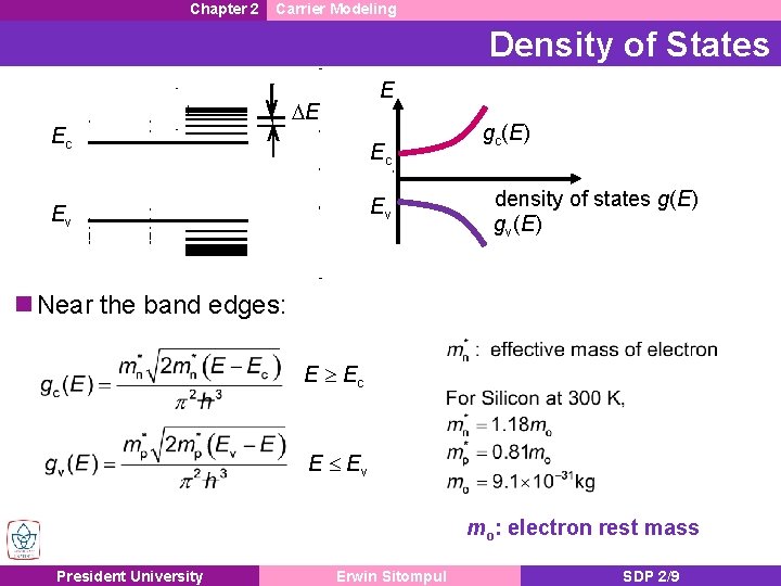
Chapter 2 Carrier Modeling Density of States Ec Ev DE E Ec Ev gc(E) density of states g(E) gv(E) n g(E) is the number of states per cm 3 per e. V. n g(E)d. E is the number of states per cm 3 in the energy range between E and E+d. E). President University Erwin Sitompul SDP 2/8

Chapter 2 Carrier Modeling Density of States Ec E DE Ec Ev Ev gc(E) density of states g(E) gv(E) n Near the band edges: E Ec E Ev mo: electron rest mass President University Erwin Sitompul SDP 2/9

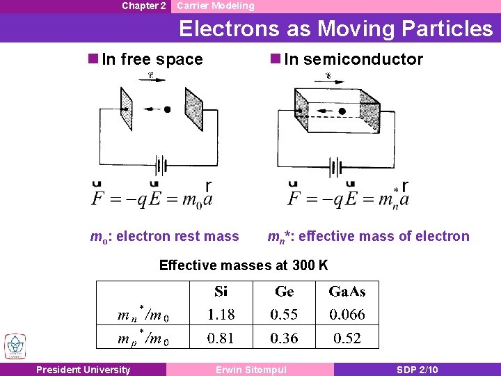
Chapter 2 Carrier Modeling Electrons as Moving Particles n In free space n In semiconductor mo: electron rest mass mn*: effective mass of electron Effective masses at 300 K President University Erwin Sitompul SDP 2/10

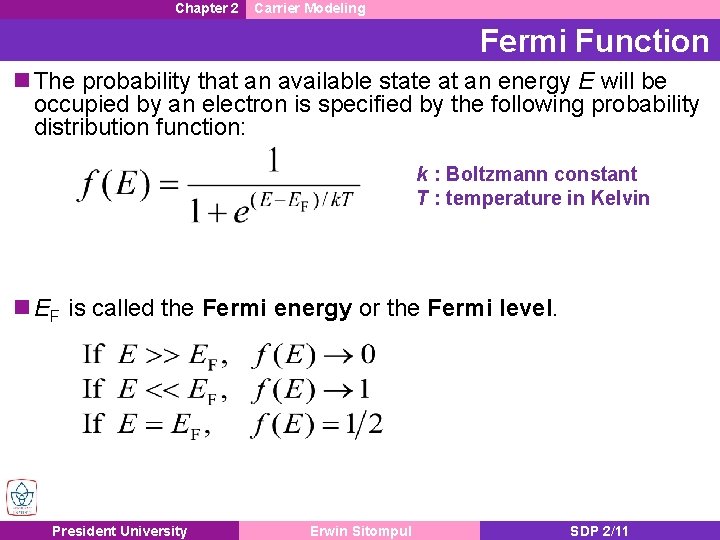
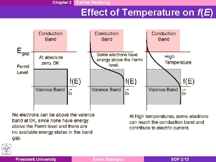
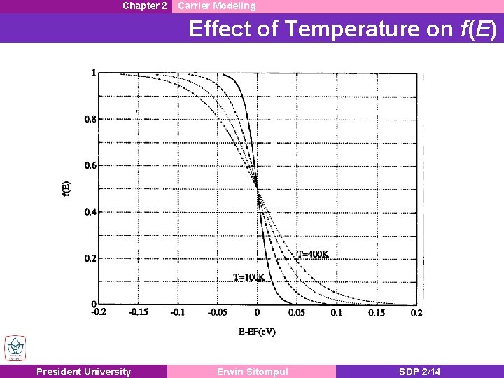
Chapter 2 Carrier Modeling Fermi Function n The probability that an available state at an energy E will be occupied by an electron is specified by the following probability distribution function: k : Boltzmann constant T : temperature in Kelvin n EF is called the Fermi energy or the Fermi level. President University Erwin Sitompul SDP 2/11

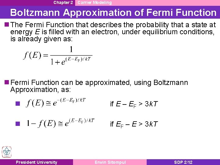
Chapter 2 Carrier Modeling Boltzmann Approximation of Fermi Function n The Fermi Function that describes the probability that a state at energy E is filled with an electron, under equilibrium conditions, is already given as: n Fermi Function can be approximated, using Boltzmann Approximation, as: n if E – EF > 3 k. T n if EF – E > 3 k. T President University Erwin Sitompul SDP 2/12

Chapter 2 Carrier Modeling Effect of Temperature on f(E) President University Erwin Sitompul SDP 2/13

Chapter 2 Carrier Modeling Effect of Temperature on f(E) President University Erwin Sitompul SDP 2/14

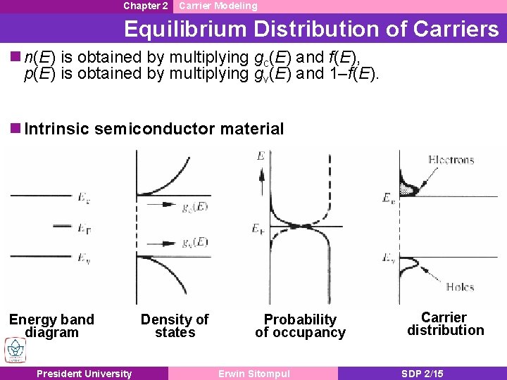
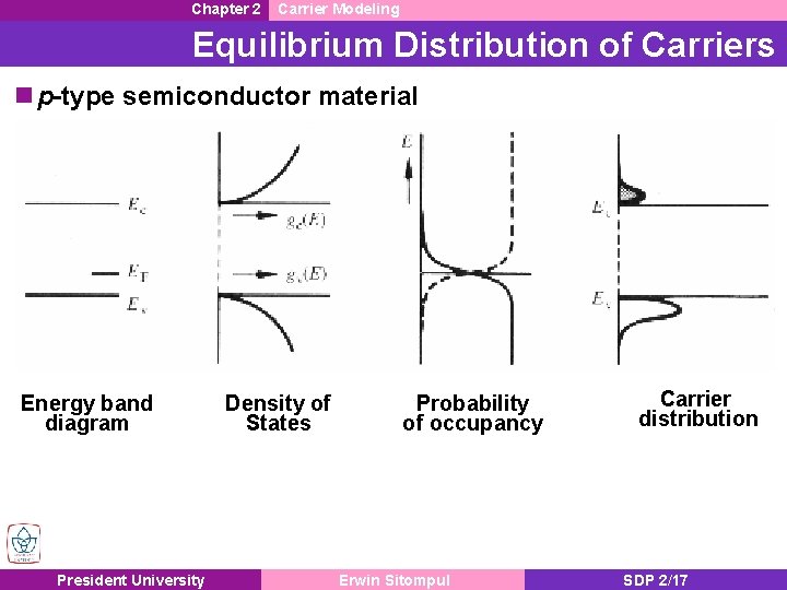
Chapter 2 Carrier Modeling Equilibrium Distribution of Carriers n n(E) is obtained by multiplying gc(E) and f(E), p(E) is obtained by multiplying gv(E) and 1–f(E). n Intrinsic semiconductor material Energy band diagram President University Density of states Probability of occupancy Erwin Sitompul Carrier distribution SDP 2/15

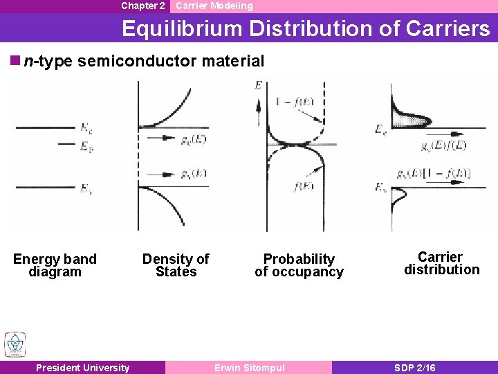
Chapter 2 Carrier Modeling Equilibrium Distribution of Carriers n n-type semiconductor material Energy band diagram President University Density of States Probability of occupancy Erwin Sitompul Carrier distribution SDP 2/16

Chapter 2 Carrier Modeling Equilibrium Distribution of Carriers n p-type semiconductor material Energy band diagram President University Density of States Probability of occupancy Erwin Sitompul Carrier distribution SDP 2/17

Chapter 2 Carrier Modeling Important Constants n Electronic charge, q = 1. 6 10– 19 C n Permittivity of free space, εo = 8. 854 10– 12 F/m n Boltzmann constant, k = 8. 62 10– 5 e. V/K n Planck constant, h = 4. 14 10– 15 e. V s n Free electron mass, mo = 9. 1 10– 31 kg n Thermal energy, k. T = 0. 02586 e. V (at 300 K) n Thermal voltage, k. T/q = 0. 02586 V (at 300 K) President University Erwin Sitompul SDP 2/18

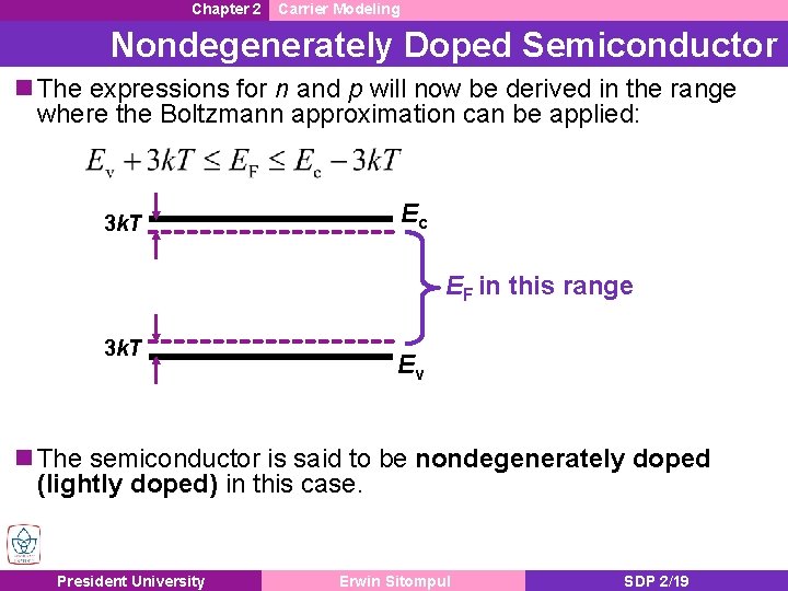
Chapter 2 Carrier Modeling Nondegenerately Doped Semiconductor n The expressions for n and p will now be derived in the range where the Boltzmann approximation can be applied: 3 k. T Ec EF in this range 3 k. T Ev n The semiconductor is said to be nondegenerately doped (lightly doped) in this case. President University Erwin Sitompul SDP 2/19

Chapter 2 Carrier Modeling Degenerately Doped Semiconductor n If a semiconductor is very heavily doped, the Boltzmann approximation is not valid. n For Si at T = 300 K, Ec-EF < 3 k. T if ND > 1. 6 1018 cm– 3 EF-Ev < 3 k. T if NA > 9. 1 1017 cm– 3 n The semiconductor is said to be degenerately doped (heavily doped) in this case. • ND = total number of donor atoms/cm 3 • NA = total number of acceptor atoms/cm 3 President University Erwin Sitompul SDP 2/20

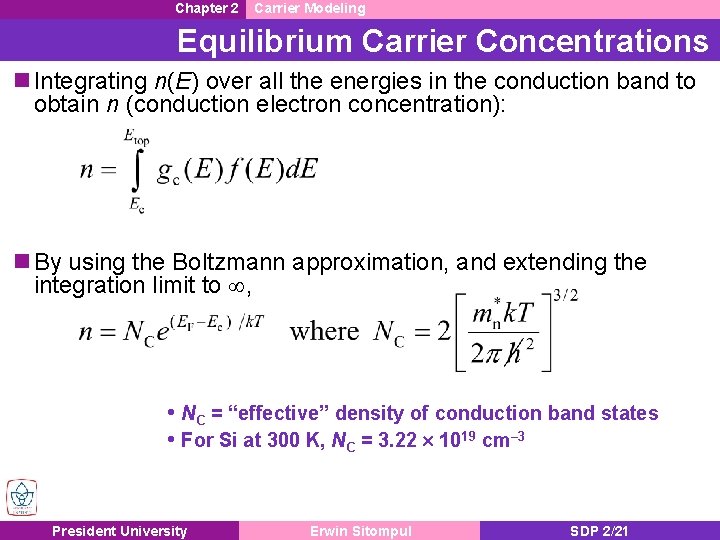
Chapter 2 Carrier Modeling Equilibrium Carrier Concentrations n Integrating n(E) over all the energies in the conduction band to obtain n (conduction electron concentration): n By using the Boltzmann approximation, and extending the integration limit to , • NC = “effective” density of conduction band states • For Si at 300 K, NC = 3. 22 1019 cm– 3 President University Erwin Sitompul SDP 2/21

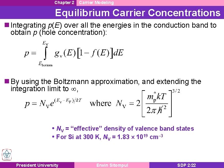
Chapter 2 Carrier Modeling Equilibrium Carrier Concentrations n Integrating p(E) over all the energies in the conduction band to obtain p (hole concentration): n By using the Boltzmann approximation, and extending the integration limit to , • NV = “effective” density of valence band states • For Si at 300 K, NV = 1. 83 1019 cm– 3 President University Erwin Sitompul SDP 2/22

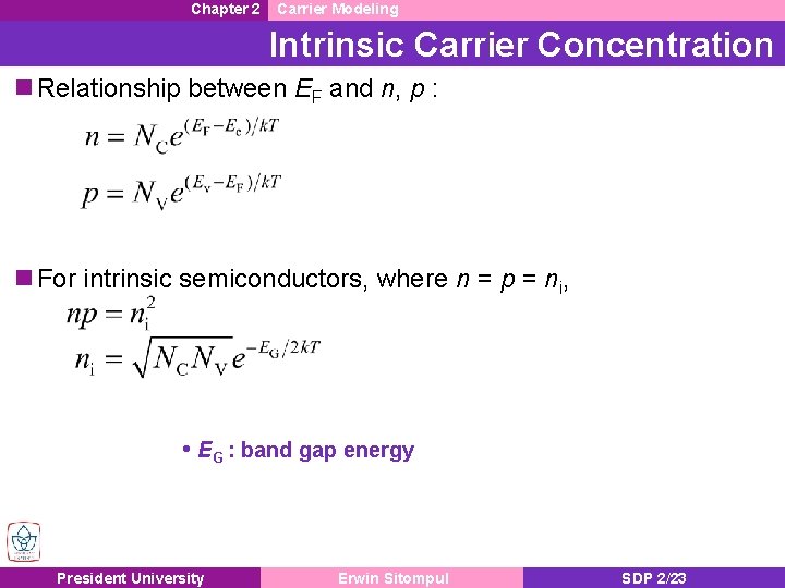
Chapter 2 Carrier Modeling Intrinsic Carrier Concentration n Relationship between EF and n, p : n For intrinsic semiconductors, where n = p = ni, • EG : band gap energy President University Erwin Sitompul SDP 2/23

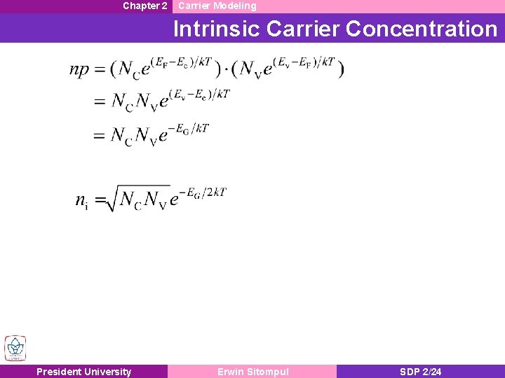
Chapter 2 Carrier Modeling Intrinsic Carrier Concentration President University Erwin Sitompul SDP 2/24

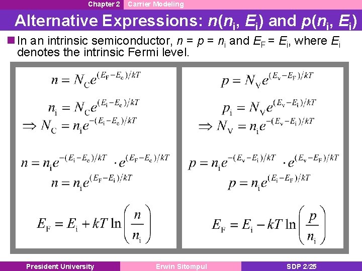
Chapter 2 Carrier Modeling Alternative Expressions: n(ni, Ei) and p(ni, Ei) n In an intrinsic semiconductor, n = p = ni and EF = Ei, where Ei denotes the intrinsic Fermi level. President University Erwin Sitompul SDP 2/25

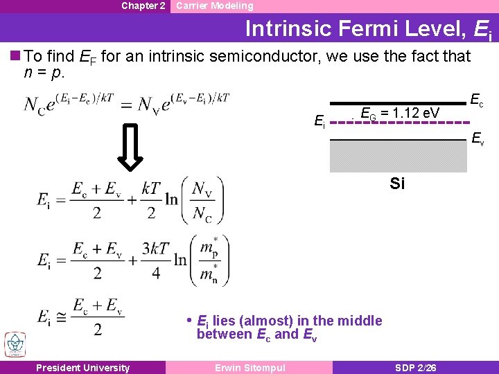
Chapter 2 Carrier Modeling Intrinsic Fermi Level, Ei n To find EF for an intrinsic semiconductor, we use the fact that n = p. Ei EG = 1. 12 e. V Ev Si • Ei lies (almost) in the middle between Ec and Ev President University Erwin Sitompul Ec SDP 2/26

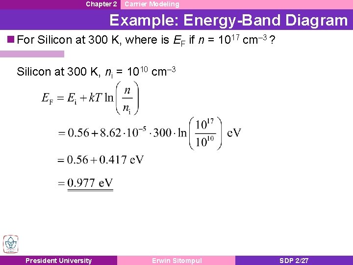
Chapter 2 Carrier Modeling Example: Energy-Band Diagram n For Silicon at 300 K, where is EF if n = 1017 cm– 3 ? Silicon at 300 K, ni = 1010 cm– 3 President University Erwin Sitompul SDP 2/27

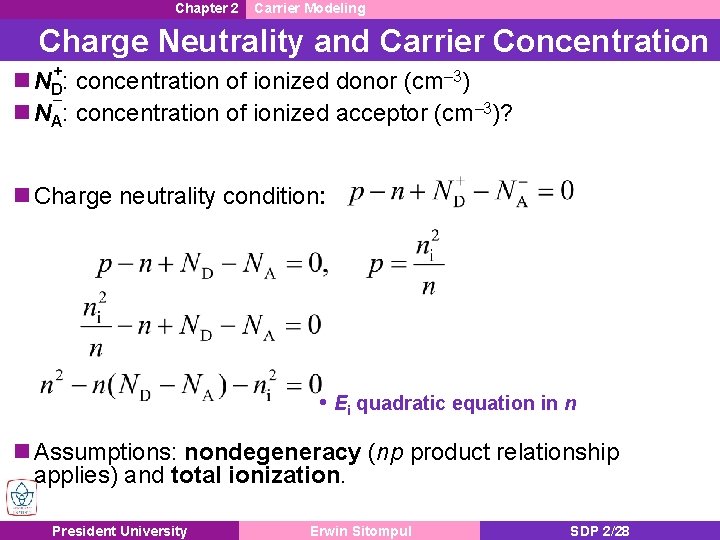
Chapter 2 Carrier Modeling Charge Neutrality and Carrier Concentration + n ND: concentration of ionized donor (cm– 3) – n NA: concentration of ionized acceptor (cm– 3)? n Charge neutrality condition: • Ei quadratic equation in n n Assumptions: nondegeneracy (np product relationship applies) and total ionization. President University Erwin Sitompul SDP 2/28

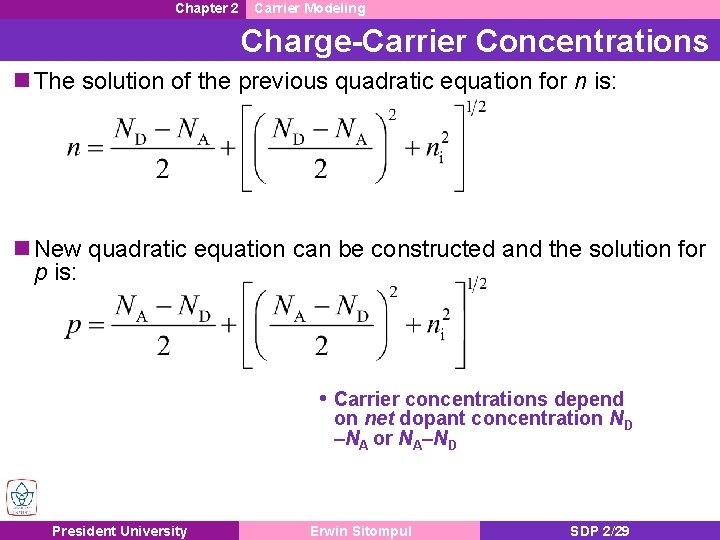
Chapter 2 Carrier Modeling Charge-Carrier Concentrations n The solution of the previous quadratic equation for n is: n New quadratic equation can be constructed and the solution for p is: • Carrier concentrations depend on net dopant concentration ND –NA or NA–ND President University Erwin Sitompul SDP 2/29

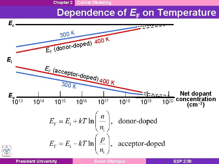
Chapter 2 Carrier Modeling Dependence of EF on Temperature Ec 300 K EF 00 K 4 ) d dope r o n o d ( Ei EF (ac ceptor -dope d) 40 0 K 300 K Ev 1013 1014 1015 President University 1016 1017 1018 Erwin Sitompul 1019 1020 Net dopant concentration (cm– 3) SDP 2/30

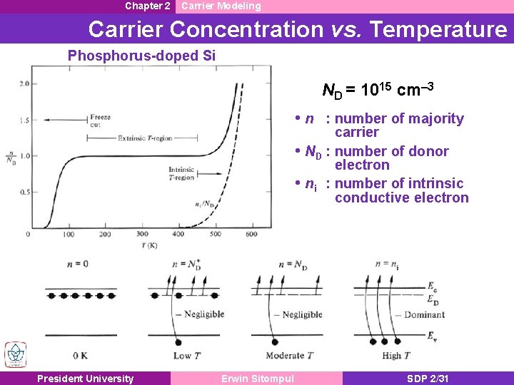
Chapter 2 Carrier Modeling Carrier Concentration vs. Temperature Phosphorus-doped Si ND = 1015 cm– 3 • n : number of majority • • President University Erwin Sitompul carrier ND : number of donor electron ni : number of intrinsic conductive electron SDP 2/31

Chapter 2 Carrier Modeling Homework 1 n 1. (Problem 2. 6 in Pierret) (4. 2) a) Under equilibrium condition at T > 0 K, what is the probability of an electron state being occupied if it is located at the Fermi level? b) If EF is positioned at Ec, determine (numerical answer required) the probability of finding electrons in states at Ec + k. T. c) The probability a state is filled at Ec + k. T is equal to the probability a state is empty at Ec + k. T. Where is the Fermi level located? n 2. (2. 36) a) Determine for what energy above EF (in terms of k. T) the Boltzmann approximation is within 1 percent of the exact Fermi probability function. b) Give the value of the exact probability function at this energy. President University Erwin Sitompul SDP 2/32

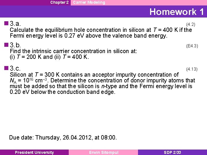
Chapter 2 Carrier Modeling Homework 1 n 3. a. (4. 2) n 3. b. (E 4. 3) n 3. c. (4. 13) Calculate the equilibrium hole concentration in silicon at T = 400 K if the Fermi energy level is 0. 27 e. V above the valence band energy. Find the intrinsic carrier concentration in silicon at: (i) T = 200 K and (ii) T = 400 K. Silicon at T = 300 K contains an acceptor impurity concentration of NA = 1016 cm– 3. Determine the concentration of donor impurity atoms that must be added so that the silicon is n-type and the Fermi energy level is 0. 20 e. V below the conduction band edge. Due date: Thursday, 26. 04. 2012, at 08: 00. President University Erwin Sitompul SDP 2/33