Semiconductor Device Physics Lecture 8 Dr Ing Erwin



- Slides: 20

Semiconductor Device Physics Lecture 8 Dr. -Ing. Erwin Sitompul President University http: //zitompul. wordpress. com 2 President University 0 1 9 Erwin Sitompul SDP 8/1

Semiconductor Device Physics Chapter 7 pn Junction Diodes: Small-Signal Admittance President University Erwin Sitompul SDP 8/2

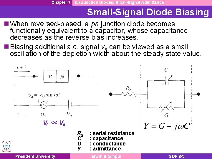
Chapter 7 pn Junction Diodes: Small-Signal Admittance Small-Signal Diode Biasing When reversed-biased, a pn junction diode becomes functionally equivalent to a capacitor, whose capacitance decreases as the reverse bias increases. Biasing additional a. c. signal va can be viewed as a small oscillation of the depletion width about the steady state value. V 0 << VA RS C G Y President University : serial resistance : capacitance : conductance : admittance Erwin Sitompul SDP 8/3

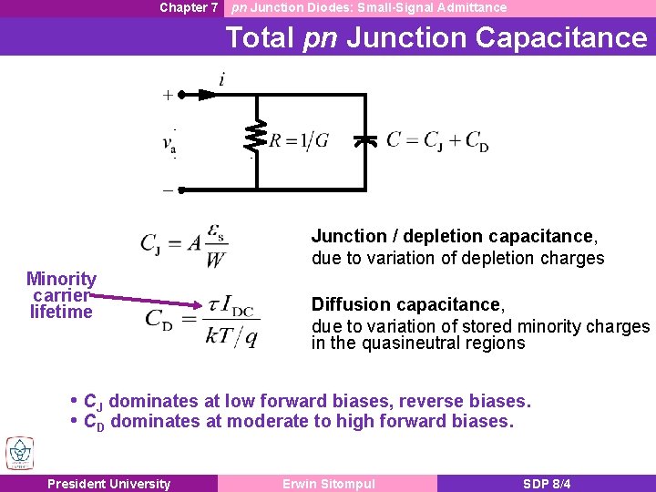
Chapter 7 pn Junction Diodes: Small-Signal Admittance Total pn Junction Capacitance Junction / depletion capacitance, due to variation of depletion charges Minority carrier lifetime Diffusion capacitance, due to variation of stored minority charges in the quasineutral regions • CJ dominates at low forward biases, reverse biases. • CD dominates at moderate to high forward biases. President University Erwin Sitompul SDP 8/4

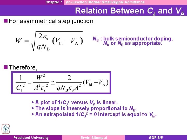
Chapter 7 pn Junction Diodes: Small-Signal Admittance Relation Between CJ and VA For asymmetrical step junction, NB : bulk semiconductor doping, NA or ND as appropriate. Therefore, • A plot of 1/CJ 2 versus VA is linear. • The slope is inversely proportional to NB. • An extrapolated 1/CJ 2 = 0 intercept is equal to Vbi. President University Erwin Sitompul SDP 8/5

Semiconductor Device Physics Chapter 8 pn Junction Diodes: Transient Response President University Erwin Sitompul SDP 8/6

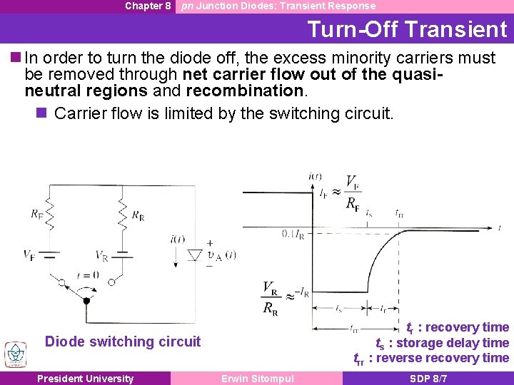
Chapter 8 pn Junction Diodes: Transient Response Turn-Off Transient In order to turn the diode off, the excess minority carriers must be removed through net carrier flow out of the quasineutral regions and recombination. Carrier flow is limited by the switching circuit. tr : recovery time ts : storage delay time trr : reverse recovery time Diode switching circuit President University Erwin Sitompul SDP 8/7

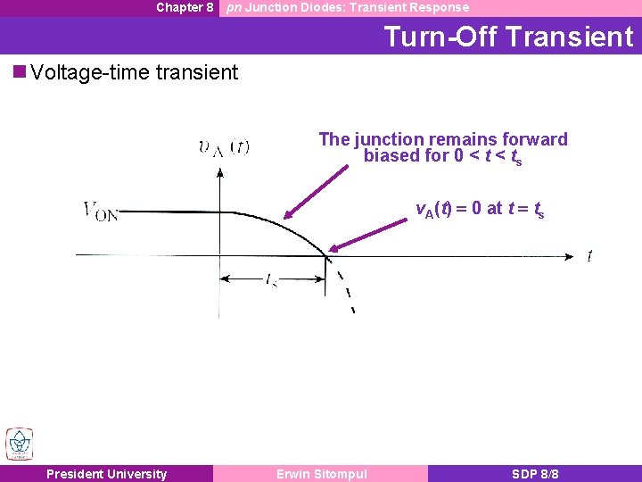
Chapter 8 pn Junction Diodes: Transient Response Turn-Off Transient Voltage-time transient The junction remains forward biased for 0 < ts v. A(t) = 0 at t = ts President University Erwin Sitompul SDP 8/8

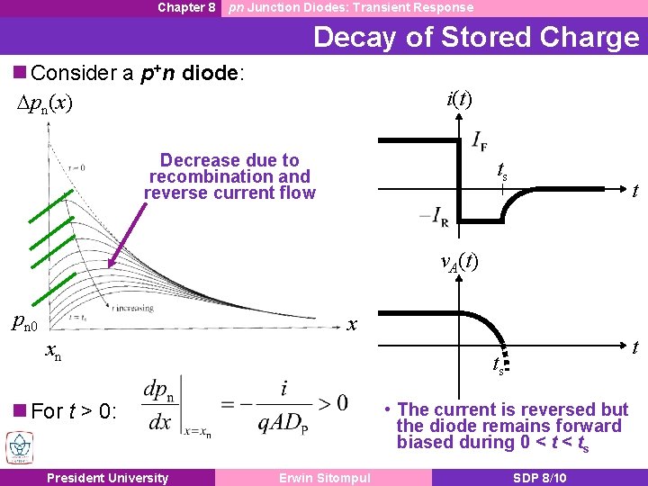
Chapter 8 pn Junction Diodes: Transient Response of pn Diode Suppose a pn diode is forward biased, then suddenly turned off at time t = 0. The excess minority carrier will be removed through recombination and reverse current flow. Because of CD, the voltage across the pn junction depletion region cannot be changed instantaneously. The delay in switching between the ON and OFF states is due to the time required to change the amount of excess minority carriers stored in the quasi-neutral regions. President University Erwin Sitompul SDP 8/9

Chapter 8 pn Junction Diodes: Transient Response Decay of Stored Charge Consider a p+n diode: Dpn(x) i(t) Decrease due to recombination and reverse current flow ts t v. A(t) pn 0 x xn ts For t > 0: President University t • The current is reversed but the diode remains forward biased during 0 < ts Erwin Sitompul SDP 8/10

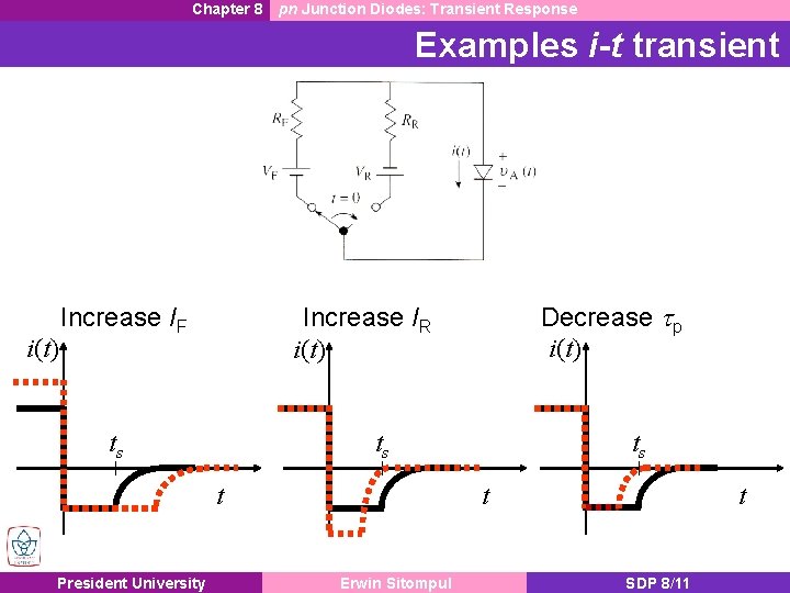
Chapter 8 pn Junction Diodes: Transient Response Examples i-t transient i(t) Increase IF ts ts t President University Decrease tp i(t) Increase IR i(t) ts t Erwin Sitompul t SDP 8/11

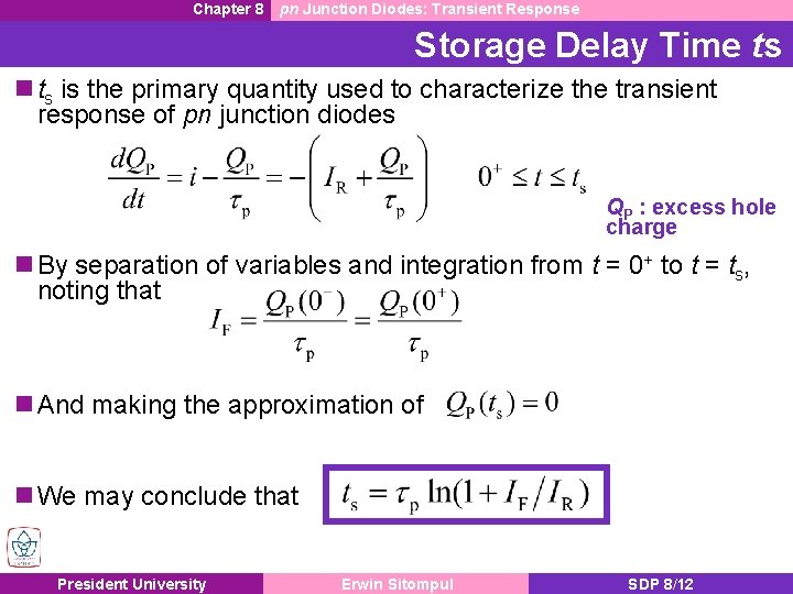
Chapter 8 pn Junction Diodes: Transient Response Storage Delay Time ts is the primary quantity used to characterize the transient response of pn junction diodes QP : excess hole charge By separation of variables and integration from t = 0+ to t = ts, noting that And making the approximation of We may conclude that President University Erwin Sitompul SDP 8/12

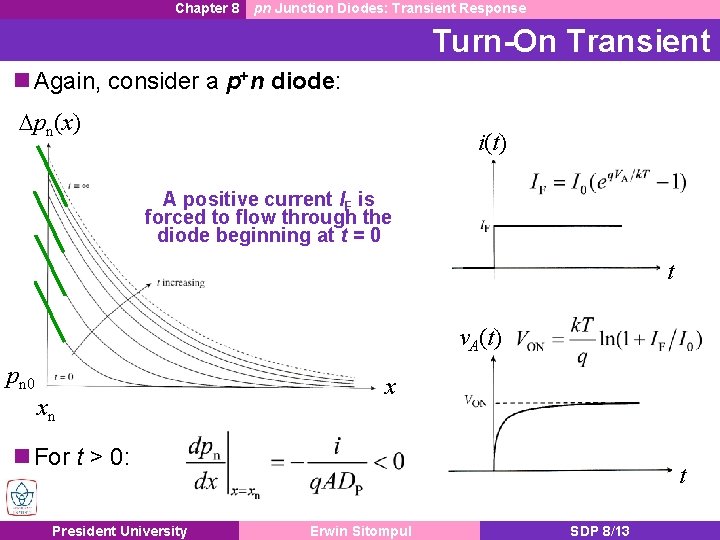
Chapter 8 pn Junction Diodes: Transient Response Turn-On Transient Again, consider a p+n diode: Dpn(x) i(t) A positive current IF is forced to flow through the diode beginning at t = 0 t v. A(t) pn 0 xn x For t > 0: President University t Erwin Sitompul SDP 8/13

Chapter 8 pn Junction Diodes: Transient Response Turn-On Transient Rewriting for turn-on characteristics, By separation of variables and integration, we have • Can you sketch QP(t)? The stored hole charge in an ideal diode is given by Steady state Finally, by assuming that the build-up of stored charge occurs quasistatically, VA v. A President University Erwin Sitompul SDP 8/14

Semiconductor Device Physics Chapter 9 Optoelectronic Diodes President University Erwin Sitompul SDP 8/15

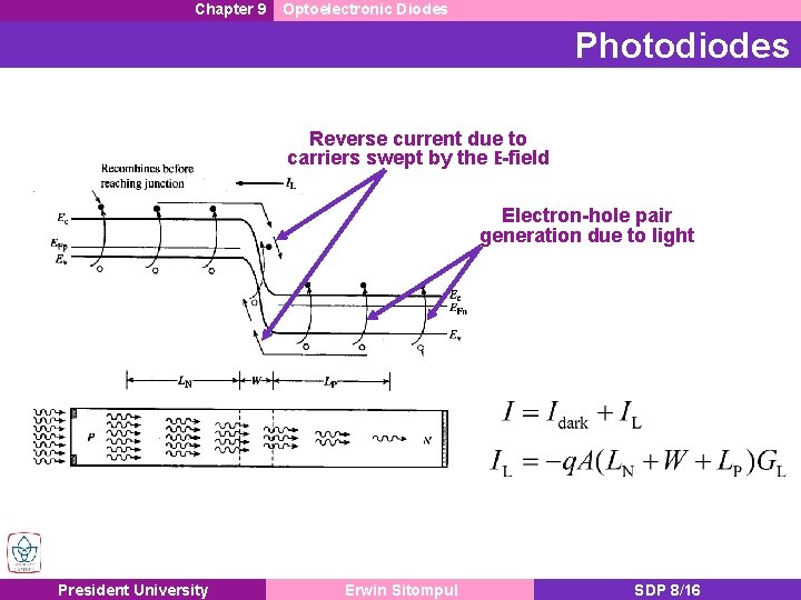
Chapter 9 Optoelectronic Diodes Photodiodes Reverse current due to carriers swept by the E-field Electron-hole pair generation due to light President University Erwin Sitompul SDP 8/16

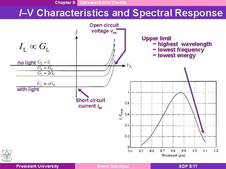
Chapter 9 Optoelectronic Diodes I–V Characteristics and Spectral Response Open circuit voltage voc Upper limit ~ highest wavelength ~ lowest frequency ~ lowest energy no light with light Short circuit current isc President University Erwin Sitompul SDP 8/17

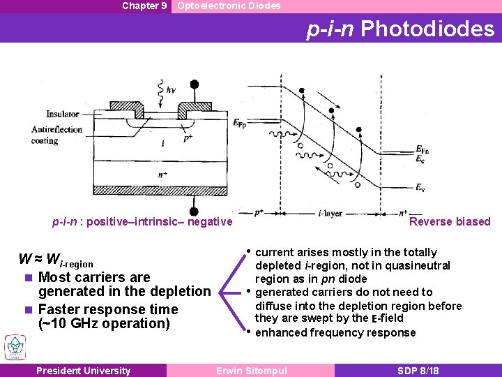
Chapter 9 Optoelectronic Diodes p-i-n Photodiodes p-i-n : positive–intrinsic– negative W ≈ Wi-region Most carriers are generated in the depletion Faster response time (~10 GHz operation) President University Reverse biased • current arises mostly in the totally • • depleted i-region, not in quasineutral region as in pn diode generated carriers do not need to diffuse into the depletion region before they are swept by the E-field enhanced frequency response Erwin Sitompul SDP 8/18

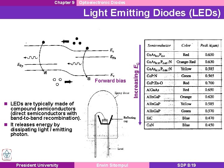
Chapter 9 Optoelectronic Diodes Forward bias Increasing EG Light Emitting Diodes (LEDs) LEDs are typically made of compound semiconductors (direct semiconductors with band-to-band recombination). It releases energy by dissipating light / emitting photon. President University Erwin Sitompul SDP 8/19

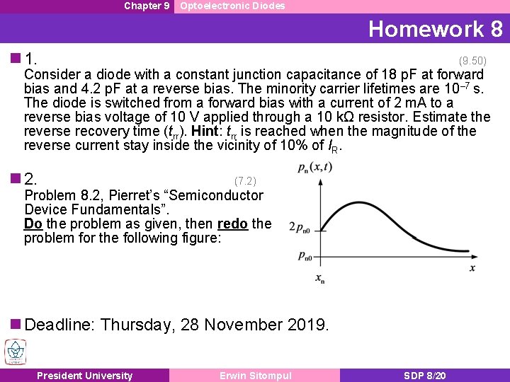
Chapter 9 Optoelectronic Diodes Homework 8 1. (9. 50) Consider a diode with a constant junction capacitance of 18 p. F at forward bias and 4. 2 p. F at a reverse bias. The minority carrier lifetimes are 10– 7 s. The diode is switched from a forward bias with a current of 2 m. A to a reverse bias voltage of 10 V applied through a 10 kΩ resistor. Estimate the reverse recovery time (trr). Hint: trr is reached when the magnitude of the reverse current stay inside the vicinity of 10% of IR. 2. (7. 2) Problem 8. 2, Pierret’s “Semiconductor Device Fundamentals”. Do the problem as given, then redo the problem for the following figure: Deadline: Thursday, 28 November 2019. President University Erwin Sitompul SDP 8/20