Scanning Tunneling Microscopy Principle of Operation and Instrumentation

![Bardeen approach Published on 1961 [PRL 6, 57] Applied to STM calculation by Tersoff Bardeen approach Published on 1961 [PRL 6, 57] Applied to STM calculation by Tersoff](https://slidetodoc.com/presentation_image_h2/5a72f6ff30ffcacc4810f64b46d042d7/image-11.jpg)
- Slides: 28

Scanning Tunneling Microscopy: Principle of Operation and Instrumentation Stefano Colonna CNR – Istituto di Struttura della Materia

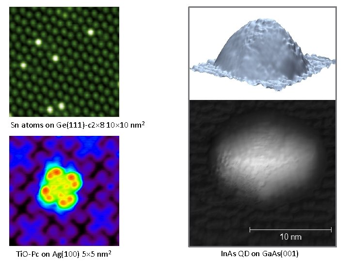
Sn atoms on Ge(111)-c 2× 8 10× 10 nm 2 Ti. O-Pc on Ag(100) 5× 5 nm 2 In. As QD on Ga. As(001)

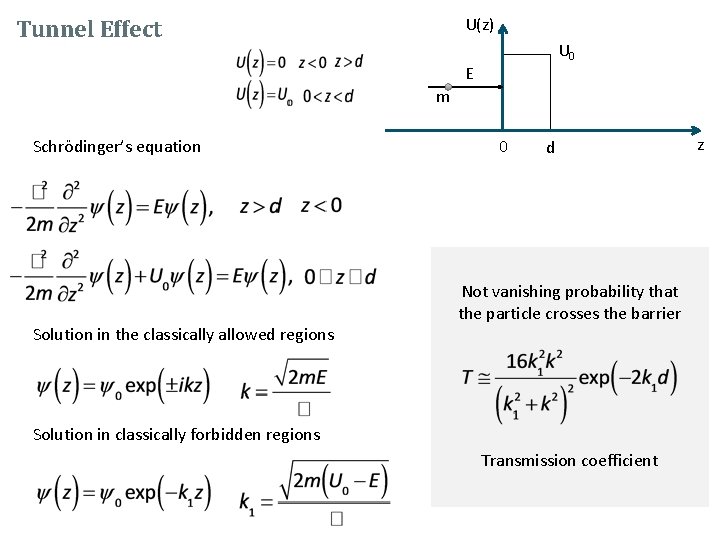
U(z) Tunnel Effect U 0 E m Schrödinger’s equation Solution in the classically allowed regions 0 d Not vanishing probability that the particle crosses the barrier Solution in classically forbidden regions Transmission coefficient z

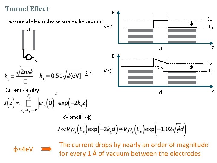
Tunnel Effect E Two metal electrodes separated by vacuum d φ V=0 EV EF z d E V Å-1 Current density V≠ 0 e. V φ EV EF d e. V small (<φ) φ≈4 e. V The current drops by nearly an order of magnitude for every 1 Å of vacuum between the electrodes z

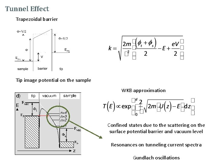
Tunnel Effect Trapezoidal barrier Tip image potential on the sample WKB approximation Confined states due to the scattering on the surface potential barrier and vacuum level Resonances on tunneling current spectra Gundlach oscillations

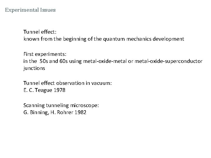
Experimental Issues Tunnel effect: known from the beginning of the quantum mechanics development First experiments: in the 50 s and 60 s using metal-oxide-metal or metal-oxide-superconductor junctions Tunnel effect observation in vacuum: E. C. Teague 1978 Scanning tunneling microscope: G. Binning, H. Rohrer 1982

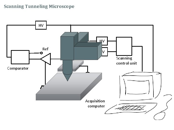
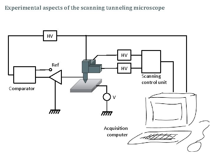
Scanning Tunneling Microscope HV HV Ref HV Scanning control unit Comparator V Acquisition computer

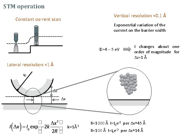
STM operation Vertical resolution ≈0. 1 Å Constant current scan Exponential variation of the current on the barrier width Φ=4 – 5 e. V I changes about one order of magnitude for Δz=1 Å R Lateral resolution ≈1 Å Δz Δx k≈1Å-1 R=1000 Å I=I 0 e-2 per Δx≅45 Å R=100 Å I=I 0 e-2 per Δx≅14 Å

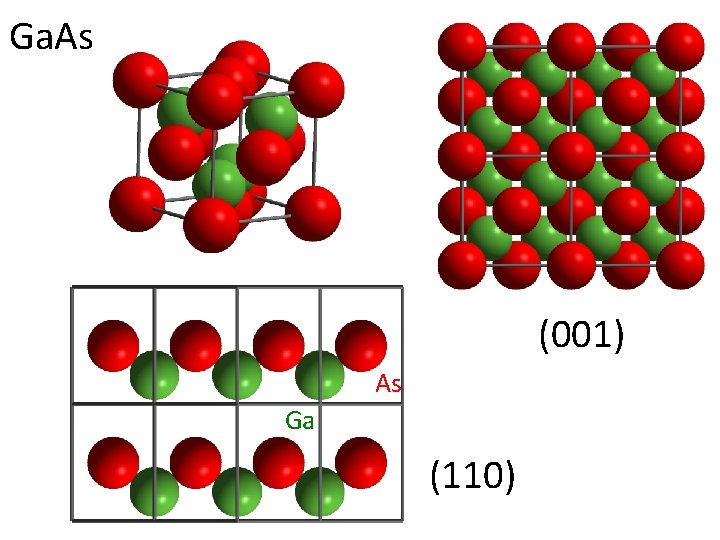
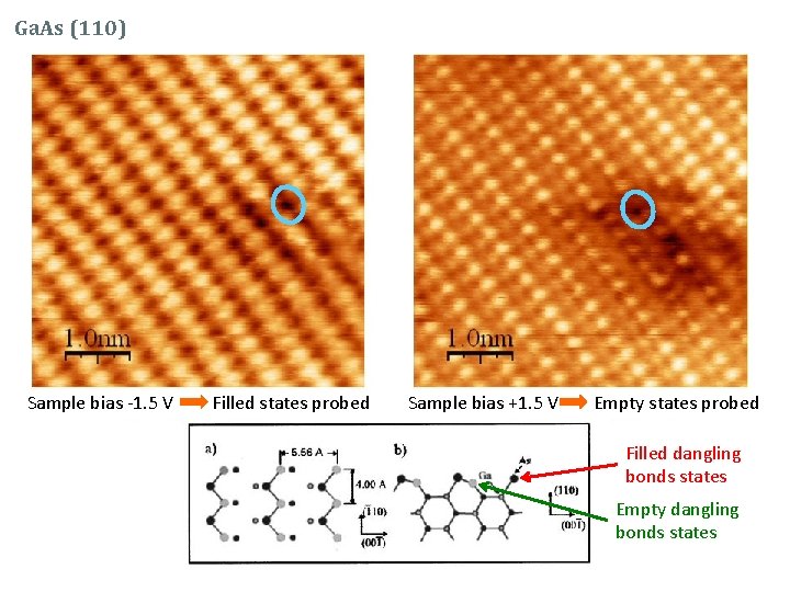
Ga. As (001) As Ga (110)

Ga. As (110) Sample bias -1. 5 V Filled states probed Sample bias +1. 5 V Empty states probed Filled dangling bonds states Empty dangling bonds states
![Bardeen approach Published on 1961 PRL 6 57 Applied to STM calculation by Tersoff Bardeen approach Published on 1961 [PRL 6, 57] Applied to STM calculation by Tersoff](https://slidetodoc.com/presentation_image_h2/5a72f6ff30ffcacc4810f64b46d042d7/image-11.jpg)
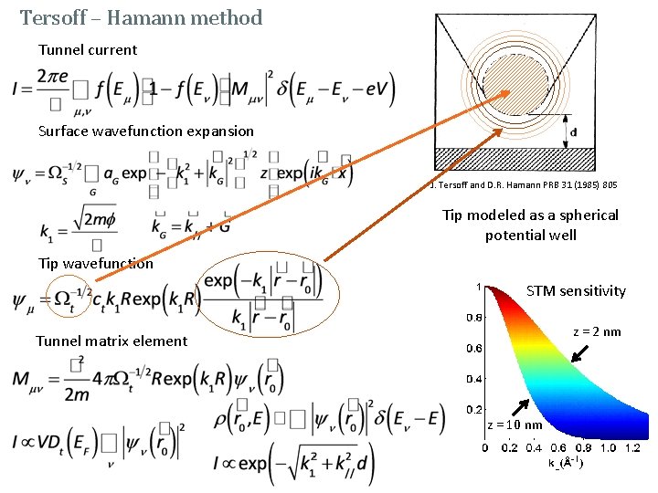
Bardeen approach Published on 1961 [PRL 6, 57] Applied to STM calculation by Tersoff and Hamann [PRL 50, 1998 / PRB 31 805] 1° order perturbation theory Tip and sample electronic states two sets of approximately orthogonal wavefunctions Approx. UT=0 Us Electron-electron interaction neglected Independent occupation probabilities of tip and sample electronic – NOT influenced by the tunneling process Approx. Us=0 Sample region U=0 UT Integration surface Small tunneling probability Perturbation approach Tip region

Tersoff – Hamann method Tunnel current Surface wavefunction expansion J. Tersoff and D. R. Hamann PRB 31 (1985) 805 Tip modeled as a spherical potential well Tip wavefunction STM sensitivity z = 2 nm Tunnel matrix element z = 10 nm

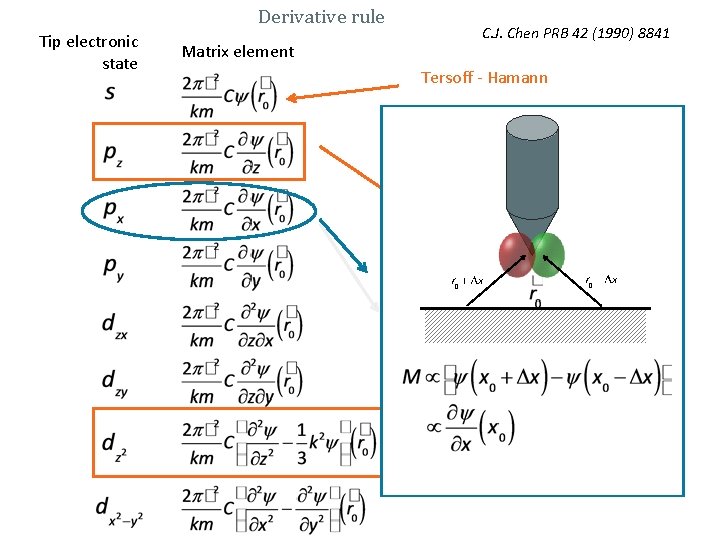
Derivative rule Tip electronic state Matrix element C. J. Chen PRB 42 (1990) 8841 Tersoff - Hamann

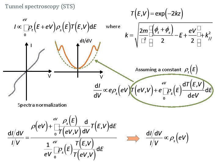
Tunnel spectroscopy (STS) where d. I/d. V I V Spectra normalization Assuming a constant V

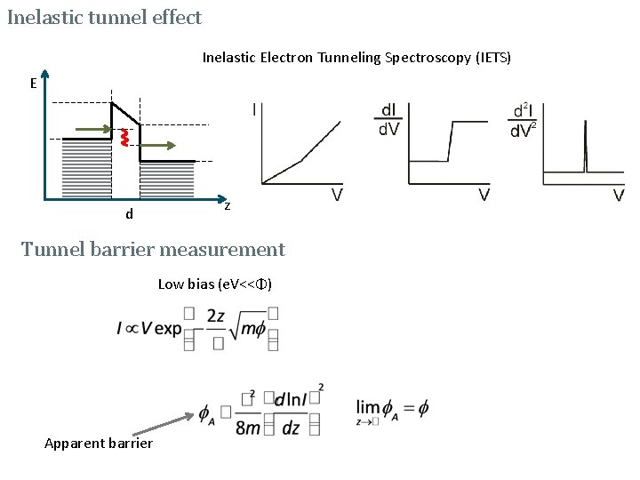
Inelastic tunnel effect Inelastic Electron Tunneling Spectroscopy (IETS) E d z Tunnel barrier measurement Low bias (e. V<<Φ) Apparent barrier

Experimental aspects of the scanning tunneling microscope HV HV Ref HV Scanning control unit Comparator V Acquisition computer

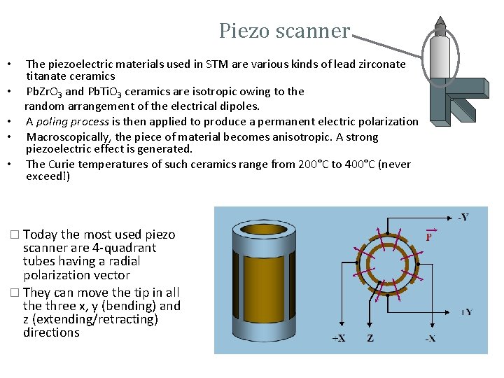
Piezo scanner • • • The piezoelectric materials used in STM are various kinds of lead zirconate titanate ceramics Pb. Zr. O 3 and Pb. Ti. O 3 ceramics are isotropic owing to the random arrangement of the electrical dipoles. A poling process is then applied to produce a permanent electric polarization Macroscopically, the piece of material becomes anisotropic. A strong piezoelectric effect is generated. The Curie temperatures of such ceramics range from 200°C to 400°C (never exceed!) � Today the most used piezo scanner are 4 -quadrant tubes having a radial polarization vector � They can move the tip in all the three x, y (bending) and z (extending/retracting) directions

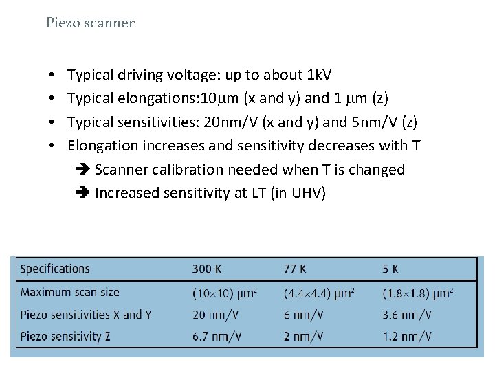
Piezo scanner • • Typical driving voltage: up to about 1 k. V Typical elongations: 10 mm (x and y) and 1 mm (z) Typical sensitivities: 20 nm/V (x and y) and 5 nm/V (z) Elongation increases and sensitivity decreases with T Scanner calibration needed when T is changed Increased sensitivity at LT (in UHV)

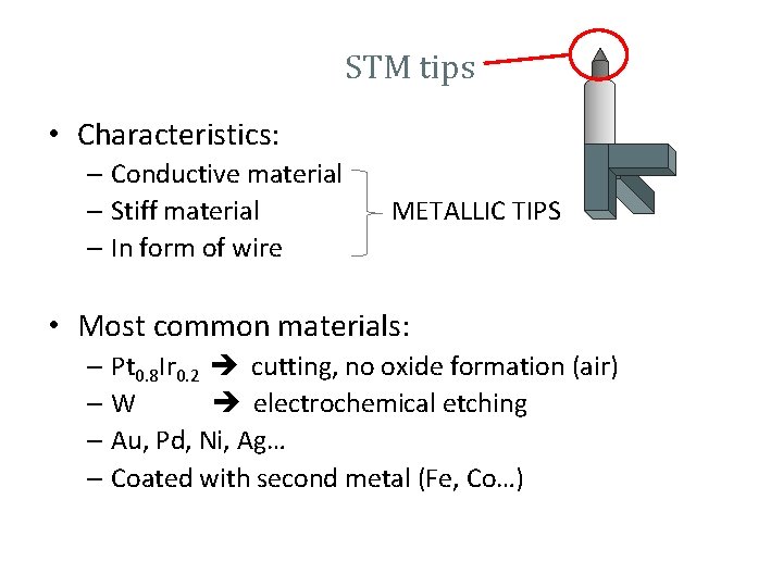
STM tips • Characteristics: – Conductive material – Stiff material – In form of wire METALLIC TIPS • Most common materials: – Pt 0. 8 Ir 0. 2 cutting, no oxide formation (air) –W electrochemical etching – Au, Pd, Ni, Ag… – Coated with second metal (Fe, Co…)

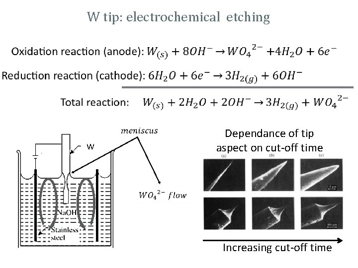
W tip: electrochemical etching • W Dependance of tip aspect on cut-off time Increasing cut-off time

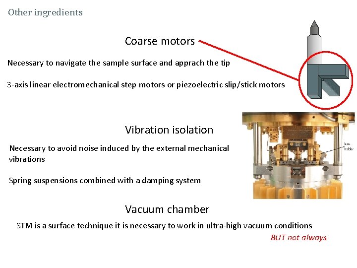
Other ingredients Coarse motors Necessary to navigate the sample surface and apprach the tip 3 -axis linear electromechanical step motors or piezoelectric slip/stick motors Vibration isolation Necessary to avoid noise induced by the external mechanical vibrations Spring suspensions combined with a damping system Vacuum chamber STM is a surface technique it is necessary to work in ultra-high vacuum conditions BUT not always

Few examples of STM measurements Not at all exhaustive

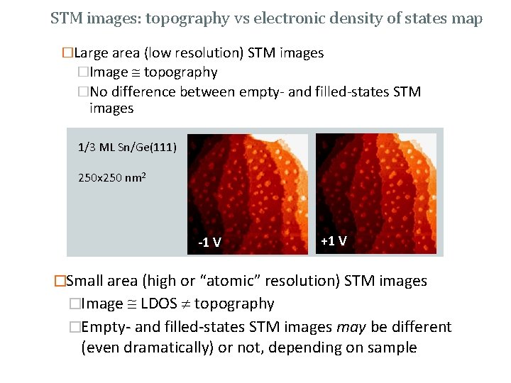
STM images: topography vs electronic density of states map �Large area (low resolution) STM images �Image topography �No difference between empty- and filled-states STM images 1/3 ML Sn/Ge(111) 250 x 250 nm 2 -1 V +1 V �Small area (high or “atomic” resolution) STM images �Image LDOS topography �Empty- and filled-states STM images may be different (even dramatically) or not, depending on sample

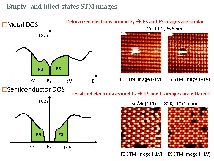
Empty- and filled-states STM images Delocalized electrons around EF ES and FS images are similar Cu(110), 5 x 5 nm �Metal DOS ES FS -e. V EF +e. V �Semiconductor DOS E -e. V ES STM image (+1 V) Localized electrons around EF ES and FS images are different DOS FS FS STM image (-1 V) Sn/Ge(111), T=80 K, 10 x 10 nm ES EF +e. V E FS STM image (-1 V) ES STM image (+1 V)

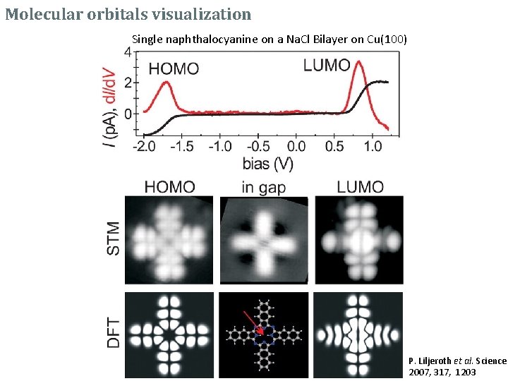
Molecular orbitals visualization Single naphthalocyanine on a Na. Cl Bilayer on Cu(100) P. Liljeroth et al. Science 2007, 317, 1203

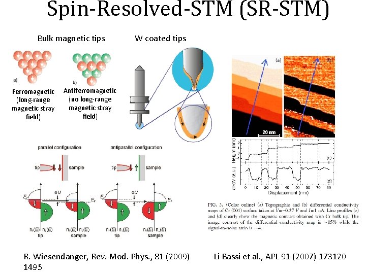
Spin-Resolved-STM (SR-STM) Bulk magnetic tips Ferromagnetic (long-range magnetic stray field) W coated tips Antiferromagnetic (no long-range magnetic stray field) R. Wiesendanger, Rev. Mod. Phys. , 81 (2009) 1495 Li Bassi et al. , APL 91 (2007) 173120

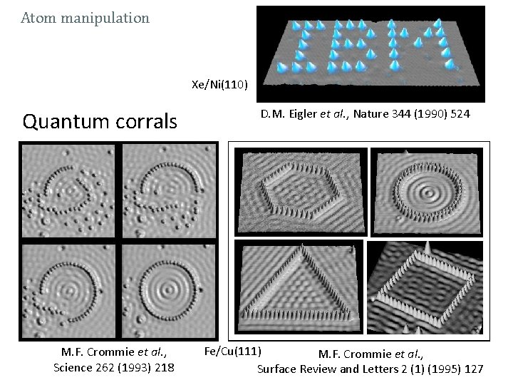
Atom manipulation Xe/Ni(110) Quantum corrals M. F. Crommie et al. , Science 262 (1993) 218 D. M. Eigler et al. , Nature 344 (1990) 524 Fe/Cu(111) M. F. Crommie et al. , Surface Review and Letters 2 (1) (1995) 127

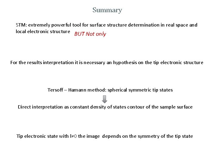
Summary STM: extremely powerful tool for surface structure determination in real space and local electronic structure BUT Not only For the results interpretation it is necessary an hypothesis on the tip electronic structure Tersoff – Hamann method: spherical symmetric tip states Direct interpretation as constant density of states contour of the sample surface Tip electronic state with l≠ 0 the image depends on the symmetry of the tip state