SCANNING PROBE MICROSCOPY SPM The invention of scanning
")
SCANNING PROBE MICROSCOPY (SPM)
, probe microscopies in general have made a")
The invention of scanning tunneling microscope (STM), probe microscopies in general have made a dramatic impact in field as diverse as material science, semiconductor, physics, biology, electrochemistry, biochemistry, surface thermodynamics, organic chemistry, catalysis, micromechanics and medical implant technology.

The reason for the nearly instantaneous acceptance of SPM is that it provides 3 -D, real space images of the surfaces at high spatial resolution. • Scanning probe microscopy (SPM) – a family of microscopic techniques that measure the morphology and properties of surfaces on atomic scale

Images are based on detecting the local interaction between a small probe tip and a surface. • SPM technologies share the concept of scanning an extremely sharp tip (3 -50 nm radius of curvature) across the object surface

Depending on the type of SPM the images can be represent: 1. Physical surface topography 2. Electronic structure 3. Electric or magnetic fields 4. A number of other local properties If a sample is clean and flat, even atoms can be imaged.

Various interactions can be studied depending on the probe sensors used. Probe Techniques The three most common scanning probe techniques are: 1. Atomic Force Microscopy (AFM) measures the interaction force between the tip and surface. The tip may be dragged across the surface, or may vibrate as it moves. 2. Scanning Tunneling Microscopy (STM) measures a weak electrical current flowing between tip and sample.
 scans a very small light source very close")
3. Near-Field Scanning Optical Microscope (NSOM) scans a very small light source very close to the sample. Detection of this light energy forms the image. NSOM can provide resolution below that of the conventional light microscope. • Other techniques: Lateral Force Microscopy(LFM) – measure relative frictional properties Magnetic Force Microscopy(MFM) – measure magnetic properties Electric Force Microscopy(EFM) – measure electrical properties

SPM allows imaging at unprecedented levels. SEM & TEM require relatively high vacuum conditions but this technology does not provide the local information about bonding that is obtained from tunneling spectroscopy.

Scanning probe micrscopy is unique among imaging techniques in that it provides 3 -D real space images And among surface analysis techniques in that it allows spatially localised measurements of structure and properties Under optimum conditions subatomic spatial resolution is achieved.

These capabilities are accomplished with an instrument that is simple in concept and design. A multimode SPM

A STM is similar to profilometer - image obtained by scanning a tip over the surface of a sample

The difference - the motion control of scanner is at Ǻ level and tip does not make contact with sample in STM –maintained at height of 5 - 50 Ǻ above the sample

Other techniques based on the same scanner principles but use various detection schemes to access a wide range of properties including atomic forces, electrostatic and magnetic forces, thermal gradient and optical density
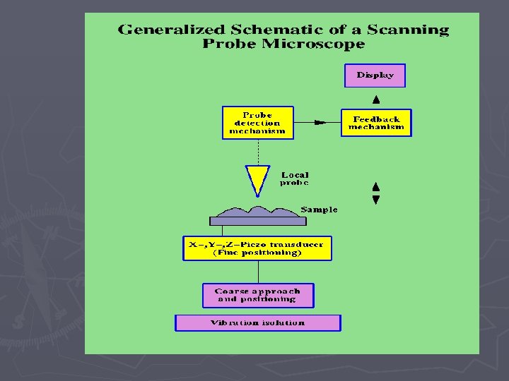

Despite the huge number of types of SPM and modes in which they can be operated the underlying operation is the same for them all

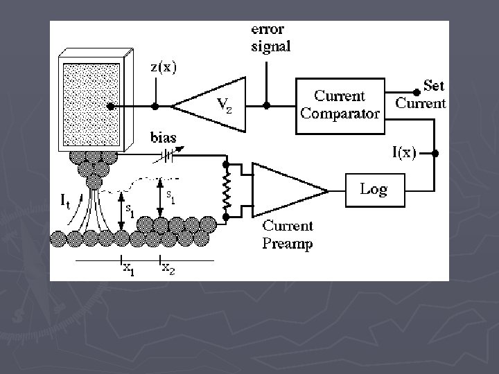
Scanning Tunneling Microscope

• STM image information – measurements of electron current that can flow when two electrodes, one sharp metal tip and relatively flat sample brought within one nanometer of each other
, electron")
• When two electrodes are so close together (a few atomic radii), electron can pass from one electrode to the other by tunneling thru the potential energy barrier • Electrically biasing the tip electrode relative to the sample allows more electron to travel in one direction , net current flow • This is probe signal, the tunneling current
")
Tunneling Current Tunneling current –originated from 1 wavelike properties of particles(electrons, in this case) When an electron incident upon a vacuum barrier with potential energy larger than the kinetic energy of the electron, thereis still a non-zero probability that it may traverse the forbidden region and reappear on the other side of the barrier.

Leak out electron wavefunction It is shown by the leak out electron wavefunction

When two conductors are so close together their leak out electron wavefunctions overlap. When a small voltage V, is applied between the tip and the sample, the overlapped electron wave function permits quantum mechanical tunneling and a current, I will flow across the vacuum gap.
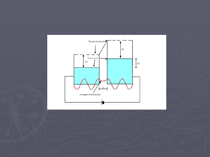

At low voltage and temperature d is the distance between the tip and sample. If the distance increased by 1 Angstrom the current flow decreased by an order of magnitude. Sensitivity to vertical distance is terribly high As the tip scans across the surface it gives atomic resolution image
-7 x 7 surface. The white spots represents the position of")
STM image of Si(111)-7 x 7 surface. The white spots represents the position of the atoms.
- Slides: 25