Scanning Electron Microscopy The Scanning Electron Microscope is


")
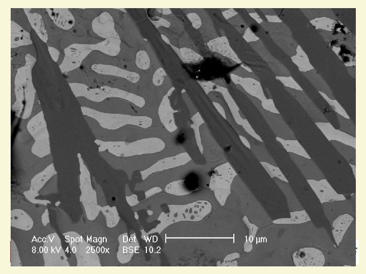
 Back-scattered electrons (High")
 Back-scattered electrons (High")
 Back-scattered electrons (High")
 Back-scattered electrons (High")
 Back-scattered electrons (High")


")
 • Secondary detectors")
 • Secondary and")
 • Secondary and")


 • Secondary and")
 analysis: • Define different grains (~0. 5 mm)")
 analysis: • Define different grains (~0. 5 mm) • Detect")
 analysis: • Define different grains (~0. 5 mm) • Detect")
 analysis: • Define different grains (~0. 5 mm) • Detect")
 analysis: • Define different grains (~0. 5 mm) • Detect")


- Slides: 43
Scanning Electron Microscopy
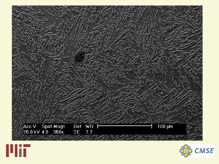
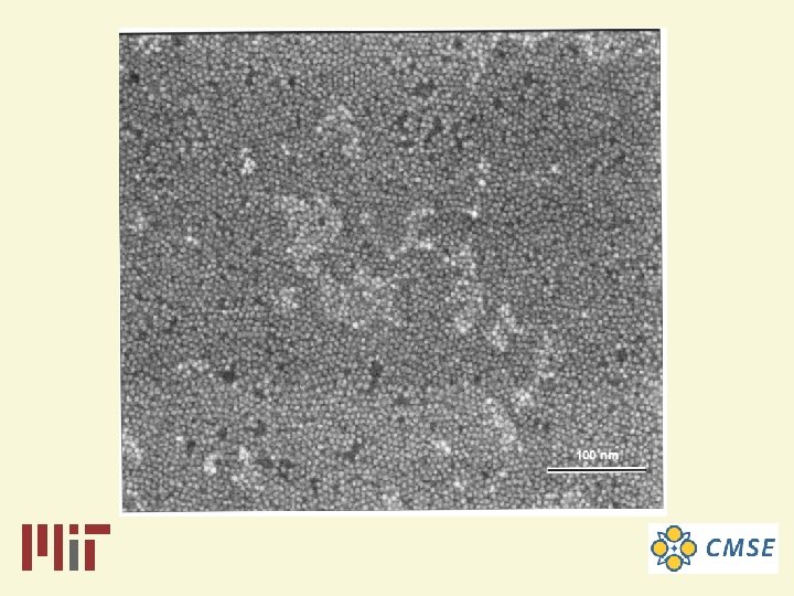
The Scanning Electron Microscope is an instrument that investigates the surfaces of solid samples.
The Scanning Electron Microscope is an instrument that investigates the surfaces of solid samples. Magnification range ~ 5 x-500, 000 x
The Scanning Electron Microscope is an instrument that investigates the surfaces of solid samples. Magnification range ~ 5 x-500, 000 x Sensitive to: • Topography
The Scanning Electron Microscope is an instrument that investigates the surfaces of solid samples. Magnification range ~ 5 x-500, 000 x Sensitive to: • Topography • Chemistry
The Scanning Electron Microscope is an instrument that investigates the surfaces of solid samples. Magnification range ~ 5 x-500, 000 x Sensitive to: • Topography • Chemistry • Crystallography
The Scanning Electron Microscope is an instrument that investigates the surfaces of solid samples. Magnification range ~ 5 x-500, 000 x Sensitive to: • Topography • Chemistry • Crystallography • Etc.
The Scanning Electron Microscope is an instrument that investigates the surfaces of solid samples. Magnification range ~ 5 x-500, 000 x Sensitive to: • Topography • Chemistry • Crystallography • Etc. Resolution down to 1 nm. point-to-point
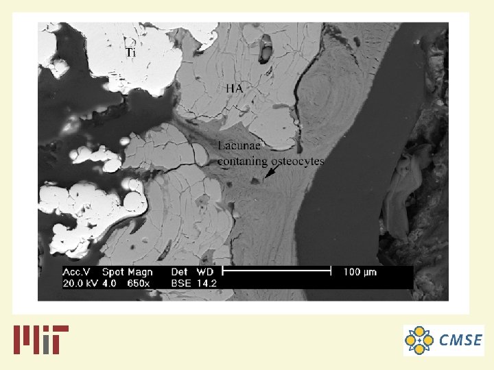
Products of interaction of electrons with matter:
Products of interaction of electrons with matter: Secondary Electrons (Low energy)
Products of interaction of electrons with matter: Secondary Electrons (Low energy) Back-scattered electrons (High energy)
Products of interaction of electrons with matter: Secondary Electrons (Low energy) Back-scattered electrons (High energy) X-rays
Products of interaction of electrons with matter: Secondary Electrons (Low energy) Back-scattered electrons (High energy) X-rays Auger electrons (Medium energy)
Products of interaction of electrons with matter: Secondary Electrons (Low energy) Back-scattered electrons (High energy) X-rays Auger electrons (Medium energy) Light
Products of interaction of electrons with matter: Secondary Electrons (Low energy) Back-scattered electrons (High energy) X-rays Auger electrons (Medium energy) Light Etc
JEOL 5910 General-Purpose SEM
FEI XL 30 FEG-ESEM
JEOL 6320 High-resolution SEM
Features of our SEMs
Features of our SEMs • Large sample chambers (6320 more restricted)
Features of our SEMs • Large sample chambers (6320 more restricted) • Secondary detectors
Features of our SEMs • Large sample chambers (6320 more restricted) • Secondary and Backscatter detectors
Features of our SEMs • Large sample chambers (6320 more restricted) • Secondary and Backscatter detectors • Energy-dispersive X-ray detectors
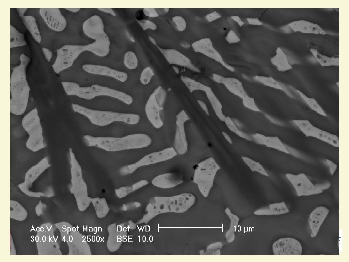
SE Cu Pb Sn
BSE Cu Pb Sn
Features of our SEMs • Large sample chambers (6320 more restricted) • Secondary and Backscatter detectors • Energy-dispersive X-ray detectors • Backscatter diffraction patterns
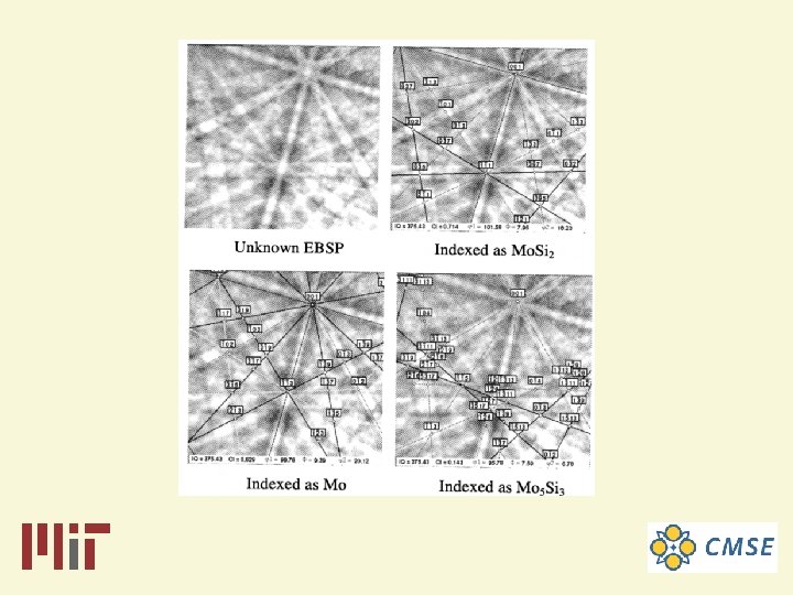
Electron Backscatter Diffraction (EBSD) analysis: • Define different grains (~0. 5 mm)
Electron Backscatter Diffraction (EBSD) analysis: • Define different grains (~0. 5 mm) • Detect Preferred orientations (texture)
Electron Backscatter Diffraction (EBSD) analysis: • Define different grains (~0. 5 mm) • Detect Preferred orientations (texture) • Measure misorientations (~1 o)
Electron Backscatter Diffraction (EBSD) analysis: • Define different grains (~0. 5 mm) • Detect Preferred orientations (texture) • Measure misorientations (~1 o) • Detect different phases
Electron Backscatter Diffraction (EBSD) analysis: • Define different grains (~0. 5 mm) • Detect Preferred orientations (texture) • Measure misorientations (~1 o) • Detect different phases • BUT – Needs VERY well prepared samples!
What else can we do? • Stereo Imaging
What else can we do? • Stereo Imaging • Height Mapping (Using Me. X software)
What else can we do? • Stereo Imaging • Height Mapping (Using Me. X software) • Feature analysis (Using Image Analysis software)
Introduction to Scanning Electron Microscopy Patrick Boisvert Thu Jan 25, 10 -11: 00 am, 13 -2137 The lecture will provide an introduction to the basic principles of Scanning Electron Microscopy with an approach to EDX, EBSD, and BSE. Contact: Patrick Boisvert, 13 -1018, x 3 -3317, pboisver@mit. edu