Scanning Tunneling Microscopy STM Short description Theory of
- Slides: 159

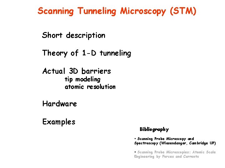
Scanning Tunneling Microscopy (STM) Short description Theory of 1 -D tunneling Actual 3 D barriers tip modeling atomic resolution Hardware Examples Bibliography • Scanning Probe Microscopy and Spectroscopy (Wiesendanger, Cambridge UP) • Scanning Probe Microscopies: Atomic Scale Engineering by Forces and Currents

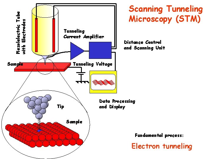
Piezolelectric Tube with Electrodes Scanning Tunneling Microscopy (STM) Tunneling Current Amplifier Sample Distance Control and Scanning Unit Tunneling Voltage Data Processing and Display Tip Sample Fundamental process: Electron tunneling

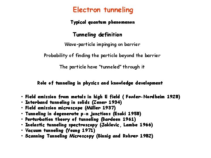
Electron tunneling Typical quantum phenomenon Tunneling definition Wave-particle impinging on barrier Probability of finding the particle beyond the barrier The particle have “tunneled” through it Role of tunneling in physics and knowledge development • • Field emission from metals in high E field ( Fowler-Nordheim 1928) Interband tunneling in solids (Zener 1934) Field emission microscope (Müller 1937) Tunneling in degenerate p-n junctions (Esaki 1958) Perturbation theory of tunneling (Bardeen 1961) Inelastic tunneling spectroscopy (Jaklevic, Lambe 1966) Vacuum tunneling (Young 1971) Scanning Tunneling Microscopy (Binnig and Rohrer 1982)

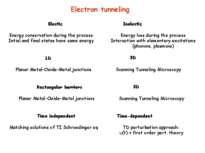
Electron tunneling Elastic Energy conservation during the process Intial and final states have same energy 1 D Planar Metal-Oxide-Metal junctions Rectangular barriers Planar Metal-Oxide-Metal junctions Time independent Matching solutions of TI Schroedinger eq Inelastic Energy loss during the process Interaction with elementary excitations (phonons, plasmons) 3 D Scanning Tunneling Microscopy Time-dependent TD perturbation approach: (t) + first order pert. theory

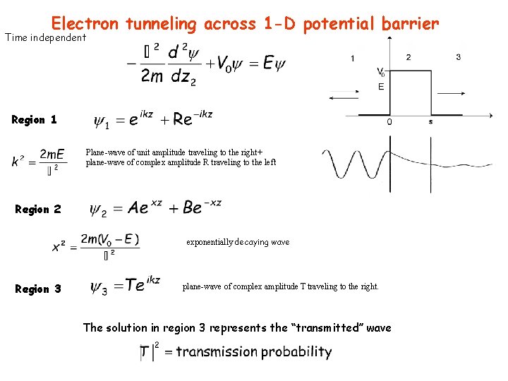
Electron tunneling across 1 -D potential barrier Time independent Region 1 Plane-wave of unit amplitude traveling to the right+ plane-wave of complex amplitude R traveling to the left Region 2 exponentially decaying wave Region 3 plane-wave of complex amplitude T traveling to the right. The solution in region 3 represents the “transmitted” wave

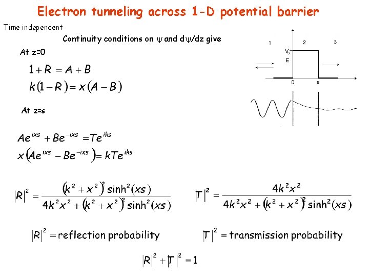
Electron tunneling across 1 -D potential barrier Time independent Continuity conditions on and d /dz give At z=0 At z=s

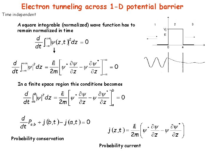
Electron tunneling across 1 -D potential barrier Time independent A square integrable (normalized) wave function has to remain normalized in time In a finite space region this conditions becomes Probability conservation Probability current

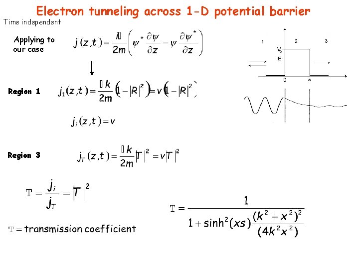
Electron tunneling across 1 -D potential barrier Time independent Applying to our case Region 1 Region 3

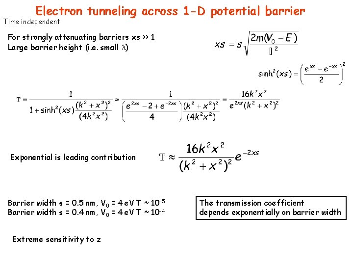
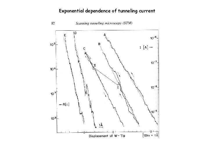
Electron tunneling across 1 -D potential barrier Time independent For strongly attenuating barriers xs >> 1 Large barrier height (i. e. small ) Exponential is leading contribution Barrier width s = 0. 5 nm, V 0 = 4 e. V T ~ 10 -5 Barrier width s = 0. 4 nm, V 0 = 4 e. V T ~ 10 -4 Extreme sensitivity to z The transmission coefficient depends exponentially on barrier width

Exponential dependence of tunneling current

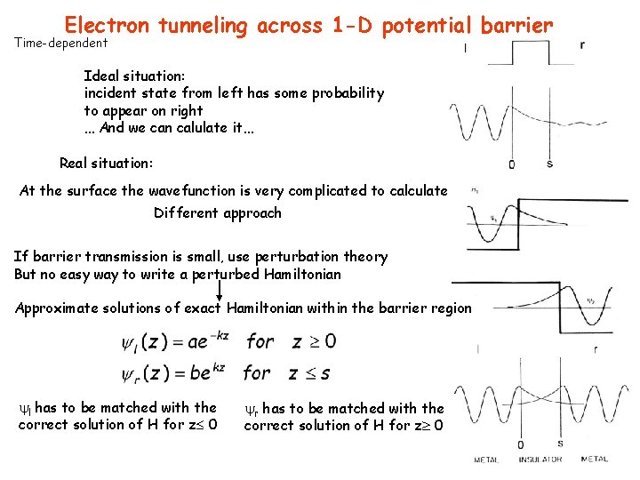
Electron tunneling across 1 -D potential barrier Time-dependent Ideal situation: incident state from left has some probability to appear on right … And we can calulate it… Real situation: At the surface the wavefunction is very complicated to calculate Different approach If barrier transmission is small, use perturbation theory But no easy way to write a perturbed Hamiltonian Approximate solutions of exact Hamiltonian within the barrier region l has to be matched with the correct solution of H for z 0 r has to be matched with the correct solution of H for z 0

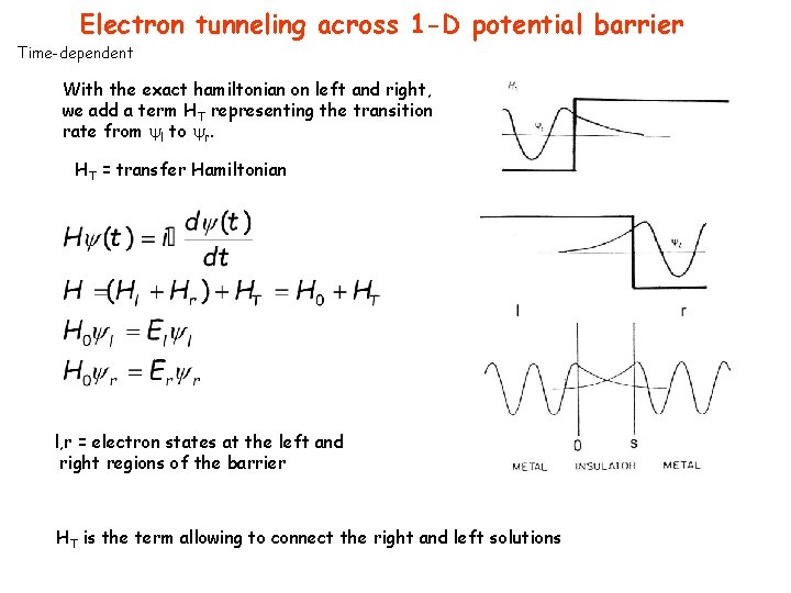
Electron tunneling across 1 -D potential barrier Time-dependent With the exact hamiltonian on left and right, we add a term HT representing the transition rate from l to r. HT = transfer Hamiltonian l, r = electron states at the left and right regions of the barrier HT is the term allowing to connect the right and left solutions

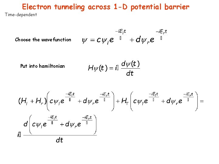
Electron tunneling across 1 -D potential barrier Time-dependent Choose the wavefunction Put into hamiltonian

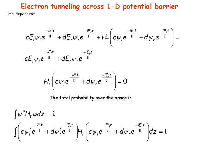
Electron tunneling across 1 -D potential barrier Time-dependent The total probability over the space is

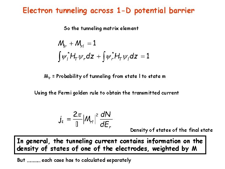
Electron tunneling across 1 -D potential barrier So the tunneling matrix element Mlr = Probability of tunneling from state l to state m Using the Fermi golden rule to obtain the transmitted current Density of states of the final state In general, the tunneling current contains information on the density of states of one of the electrodes, weighted by M But ………… each case has to calculated separately

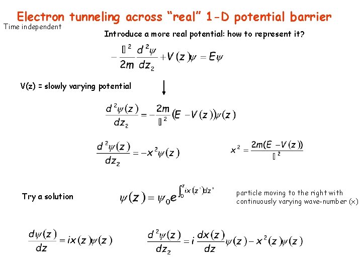
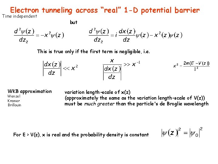
Electron tunneling across “real” 1 -D potential barrier Time independent Introduce a more real potential: how to represent it? V(z) = slowly varying potential Try a solution particle moving to the right with continuously varying wave-number (x)

Electron tunneling across “real” 1 -D potential barrier Time independent but This is true only if the first term is negligible, i. e. WKB approximation Wenzel Kramer Brillouin variation length-scale of x(z) (approximately the same as the variation length-scale of V(z)) must be much greater than the particle's de Broglie wavelength For E > V(z), x is real and the probability density is constant

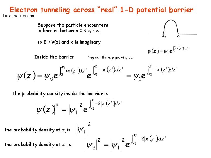
Electron tunneling across “real” 1 -D potential barrier Time independent Suppose the particle encounters a barrier between 0 < z 1 < z 2 so E < V(z) and x is imaginary Inside the barrier Neglect the exp growing part the probability density inside the barrier is the probability density at z 1 is the probability density at z 2 is

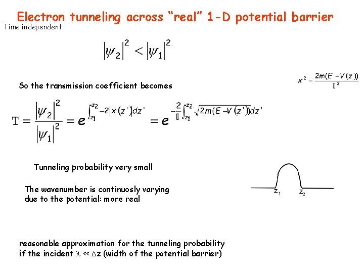
Electron tunneling across “real” 1 -D potential barrier Time independent So the transmission coefficient becomes Tunneling probability very small The wavenumber is continuosly varying due to the potential: more real reasonable approximation for the tunneling probability if the incident << z (width of the potential barrier)

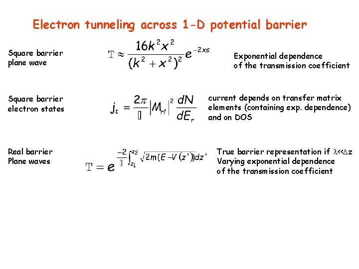
Electron tunneling across 1 -D potential barrier Square barrier plane wave Exponential dependence of the transmission coefficient Square barrier electron states current depends on transfer matrix elements (containing exp. dependence) and on DOS Real barrier Plane waves True barrier representation if << z Varying exponential dependence of the transmission coefficient

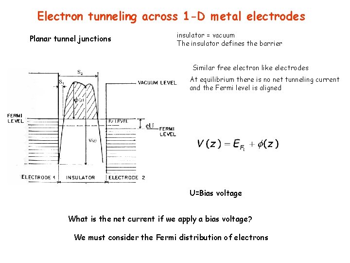
Electron tunneling across 1 -D metal electrodes Planar tunnel junctions insulator = vacuum The insulator defines the barrier Similar free electron like electrodes At equilibrium there is no net tunneling current and the Fermi level is aligned U=Bias voltage What is the net current if we apply a bias voltage? We must consider the Fermi distribution of electrons

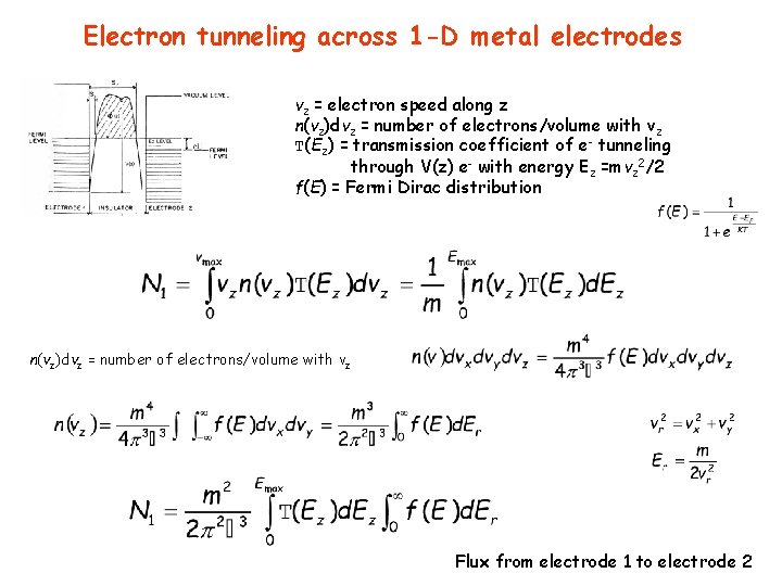
Electron tunneling across 1 -D metal electrodes vz = electron speed along z n(vz)dvz = number of electrons/volume with vz T(Ez) = transmission coefficient of e- tunneling through V(z) e- with energy Ez =mvz 2/2 f(E) = Fermi Dirac distribution n(vz)dvz = number of electrons/volume with vz Flux from electrode 1 to electrode 2

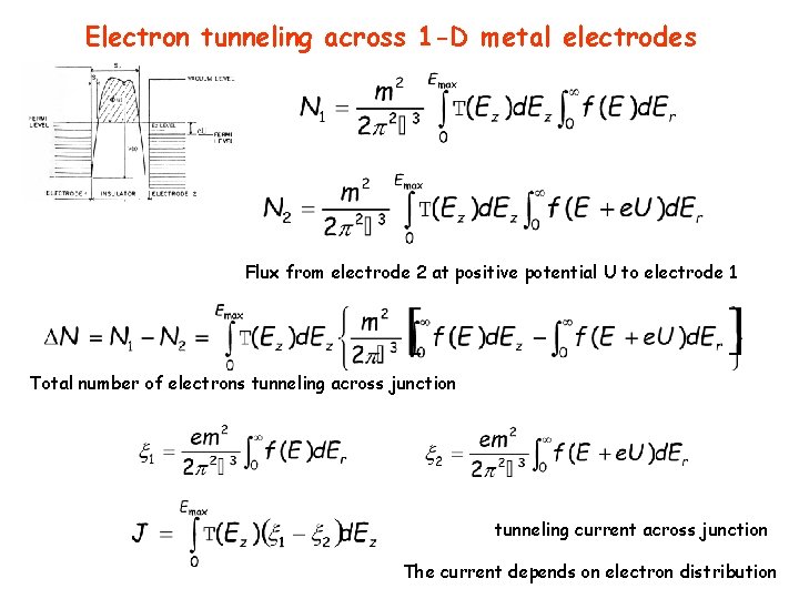
Electron tunneling across 1 -D metal electrodes Flux from electrode 2 at positive potential U to electrode 1 Total number of electrons tunneling across junction tunneling current across junction The current depends on electron distribution

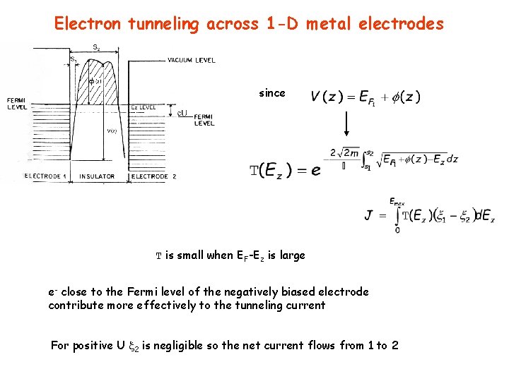
Electron tunneling across 1 -D metal electrodes since T is small when EF-Ez is large e- close to the Fermi level of the negatively biased electrode contribute more effectively to the tunneling current For positive U 2 is negligible so the net current flows from 1 to 2

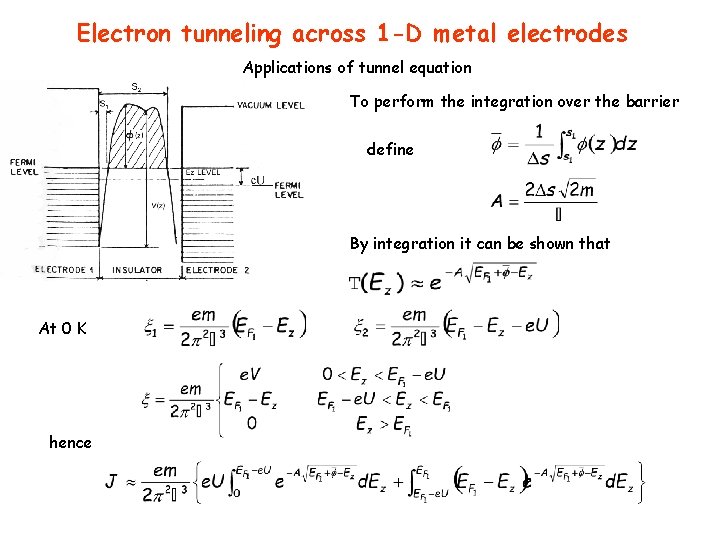
Electron tunneling across 1 -D metal electrodes Applications of tunnel equation To perform the integration over the barrier define By integration it can be shown that At 0 K hence

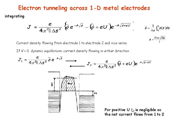
Electron tunneling across 1 -D metal electrodes integrating Current density flowing from electrode 1 to electrode 2 and vice versa If V = 0 dynamic equilibrium: current density flowing in either direction For positive U 2 is negligible so the net current flows from 1 to 2

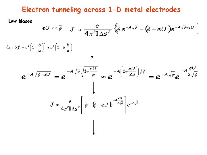
Electron tunneling across 1 -D metal electrodes Low biases

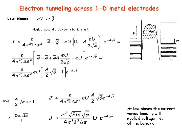
Electron tunneling across 1 -D metal electrodes Low biases Neglect second order contributions in U since At low biases the current varies linearly with applied voltage, i. e. Ohmic behavior

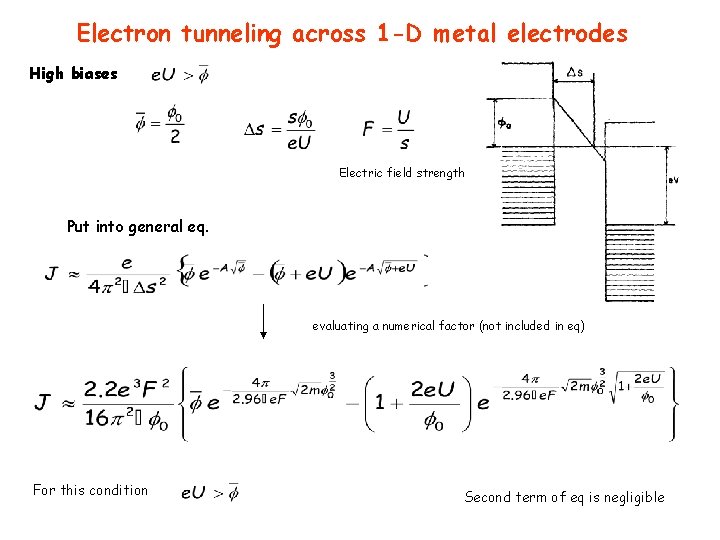
Electron tunneling across 1 -D metal electrodes High biases Electric field strength Put into general eq. evaluating a numerical factor (not included in eq) For this condition Second term of eq is negligible

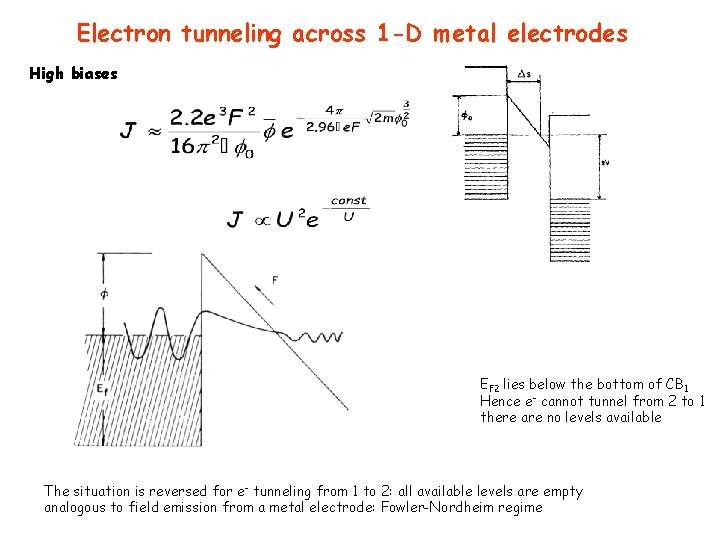
Electron tunneling across 1 -D metal electrodes High biases EF 2 lies below the bottom of CB 1 Hence e- cannot tunnel from 2 to 1 there are no levels available The situation is reversed for e- tunneling from 1 to 2: all available levels are empty analogous to field emission from a metal electrode: Fowler-Nordheim regime

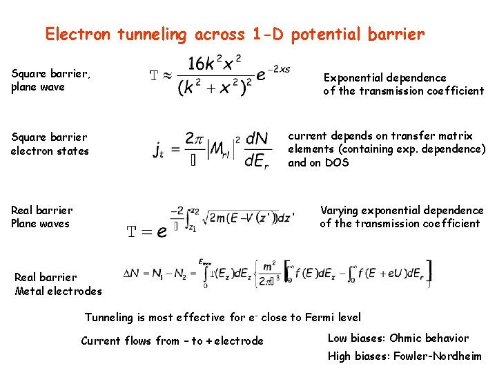
Electron tunneling across 1 -D potential barrier Square barrier, plane wave Exponential dependence of the transmission coefficient Square barrier electron states current depends on transfer matrix elements (containing exp. dependence) and on DOS Real barrier Plane waves Varying exponential dependence of the transmission coefficient Real barrier Metal electrodes Tunneling is most effective for e- close to Fermi level Current flows from – to + electrode Low biases: Ohmic behavior High biases: Fowler-Nordheim

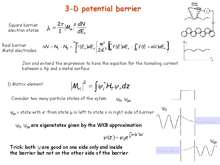
3 -D potential barrier Square barrier electron states Real barrier Metal electrodes Join and extend the expression to have the equation for the tunneling current between a tip and a metal surface 1) Matrix element Consider two many particle states of the sytem 0, = state with e- from state in left to state in right side of barrier 0 0, are eigenstates given by the WKB approximation Trick: both are good on one side only and inside the barrier but not on the other side of the barrier

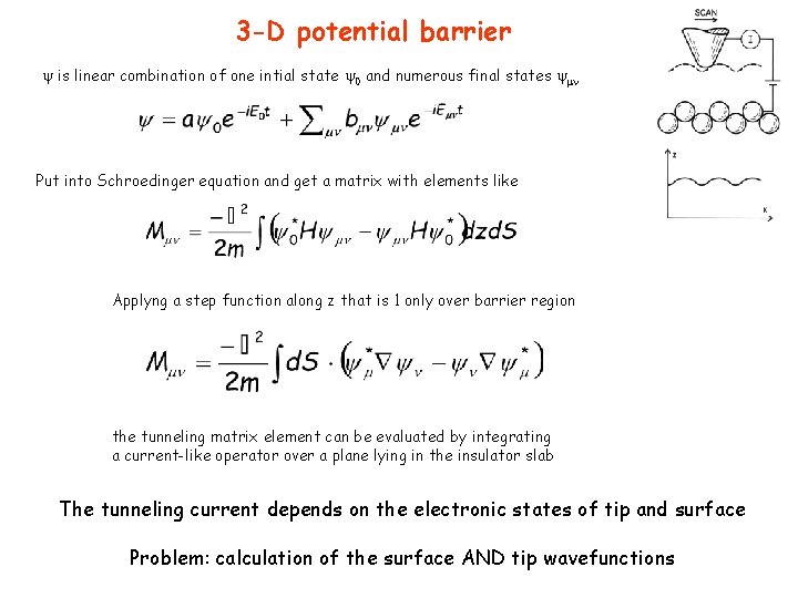
3 -D potential barrier is linear combination of one intial state 0 and numerous final states Put into Schroedinger equation and get a matrix with elements like Applyng a step function along z that is 1 only over barrier region the tunneling matrix element can be evaluated by integrating a current-like operator over a plane lying in the insulator slab The tunneling current depends on the electronic states of tip and surface Problem: calculation of the surface AND tip wavefunctions

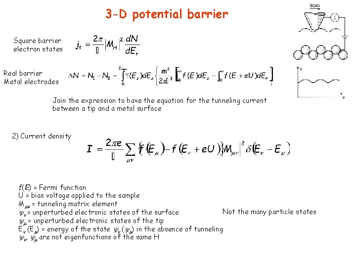
3 -D potential barrier Square barrier electron states Real barrier Metal electrodes Join the expression to have the equation for the tunneling current between a tip and a metal surface 2) Current density f(E) = Fermi function U = bias voltage applied to the sample M = tunneling matrix element Not the many particle states = unperturbed electronic states of the surface = unperturbed electronic states of the tip E (E ) = energy of the state ( ) in the absence of tunneling , are not eigenfunctions of the same H

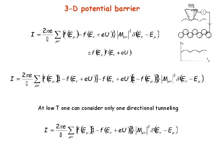
3 -D potential barrier At low T one can consider only one directional tunneling

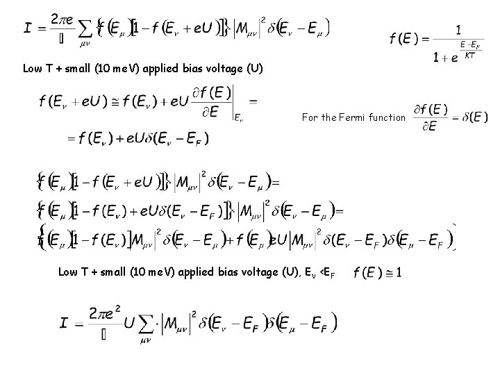
Low T + small (10 me. V) applied bias voltage (U) For the Fermi function Low T + small (10 me. V) applied bias voltage (U), E <EF

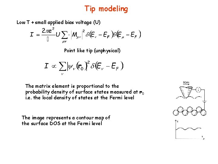
Tip modeling Low T + small applied bias voltage (U) Point like tip (unphysical) The matrix element is proportional to the probability density of surface states measured at r 0 i. e. the local density of states at the Fermi level The image represents a contour map of the surface DOS at the Fermi level

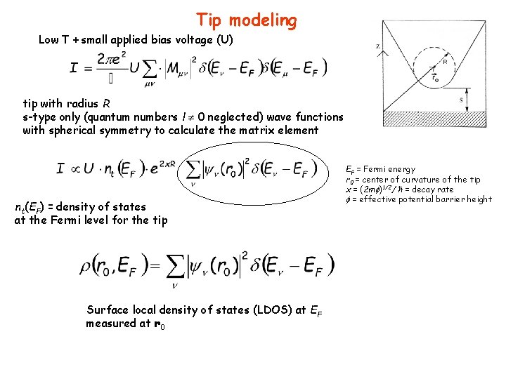
Tip modeling Low T + small applied bias voltage (U) tip with radius R s-type only (quantum numbers l 0 neglected) wave functions with spherical symmetry to calculate the matrix element nt(EF) = density of states at the Fermi level for the tip Surface local density of states (LDOS) at EF measured at r 0 EF = Fermi energy r 0 = center of curvature of the tip x = (2 m )1/2/ ħ = decay rate = effective potential barrier height

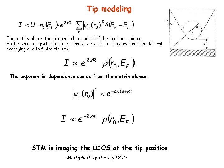
Tip modeling The matrix element is integrated in a point of the barrier region s So the value of at r 0 is no physically relevant, but it represents the lateral averaging due to finite tip size The exponential dependence comes from the matrix element STM is imaging the LDOS at the tip position Multiplied by the tip DOS

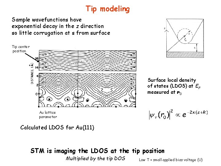
Tip modeling Sample wavefunctions have exponential decay in the z direction so little corrugation at s from surface Tip center position Surface local density of states (LDOS) at EF measured at r 0 Au lattice parameter Calculated LDOS for Au(111) STM is imaging the LDOS at the tip position Multiplied by the tip DOS Low T + small applied bias voltage (U)

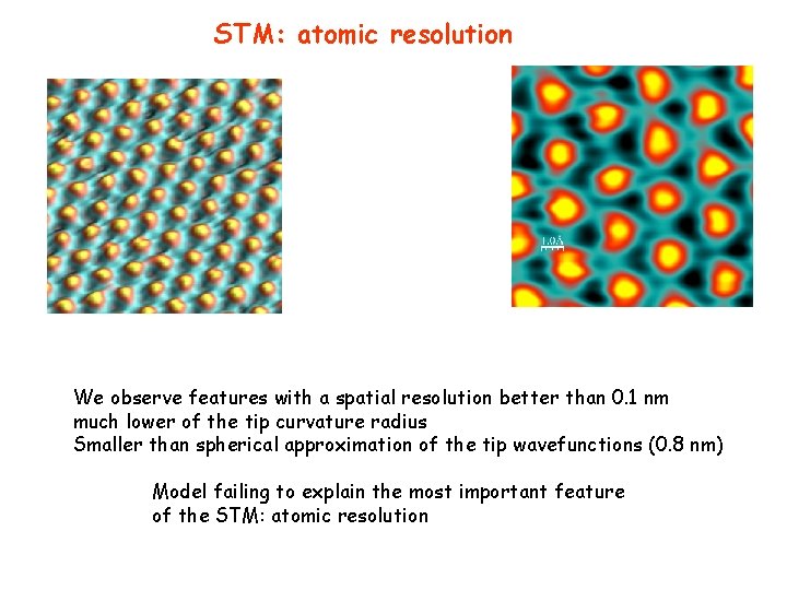
STM: atomic resolution We observe features with a spatial resolution better than 0. 1 nm much lower of the tip curvature radius Smaller than spherical approximation of the tip wavefunctions (0. 8 nm) Model failing to explain the most important feature of the STM: atomic resolution

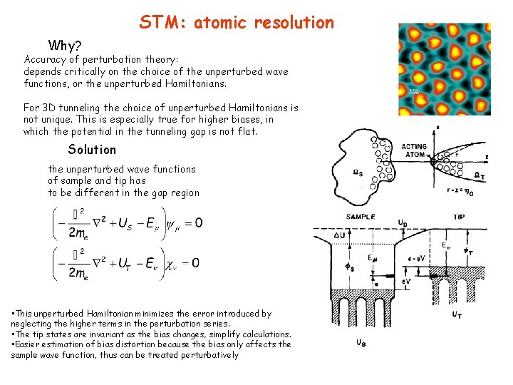
STM: atomic resolution Why? Accuracy of perturbation theory: depends critically on the choice of the unperturbed wave functions, or the unperturbed Hamiltonians. For 3 D tunneling the choice of unperturbed Hamiltonians is not unique. This is especially true for higher biases, in which the potential in the tunneling gap is not flat. Solution the unperturbed wave functions of sample and tip has to be different in the gap region • This unperturbed Hamiltonian minimizes the error introduced by neglecting the higher terms in the perturbation series. • The tip states are invariant as the bias changes, simplify calculations. • Easier estimation of bias distortion because the bias only affects the sample wave function, thus can be treated perturbatively

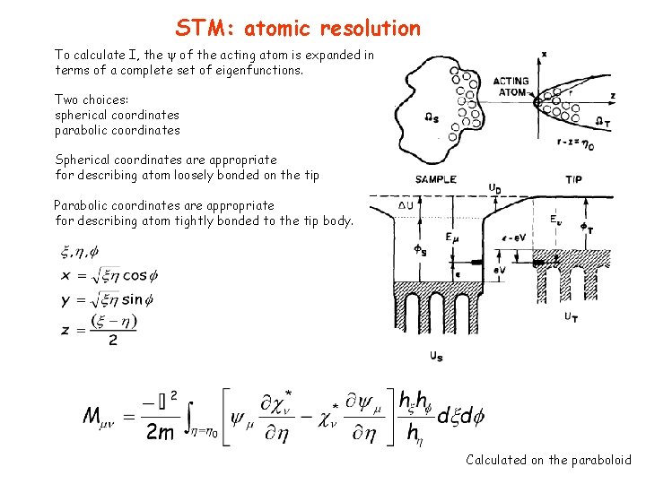
STM: atomic resolution To calculate I, the of the acting atom is expanded in terms of a complete set of eigenfunctions. Two choices: spherical coordinates parabolic coordinates Spherical coordinates are appropriate for describing atom loosely bonded on the tip Parabolic coordinates are appropriate for describing atom tightly bonded to the tip body. Calculated on the paraboloid

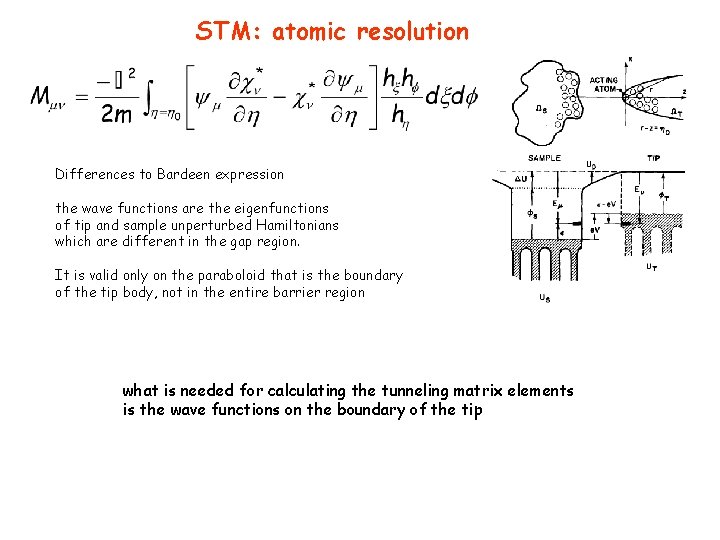
STM: atomic resolution Differences to Bardeen expression the wave functions are the eigenfunctions of tip and sample unperturbed Hamiltonians which are different in the gap region. It is valid only on the paraboloid that is the boundary of the tip body, not in the entire barrier region what is needed for calculating the tunneling matrix elements is the wave functions on the boundary of the tip

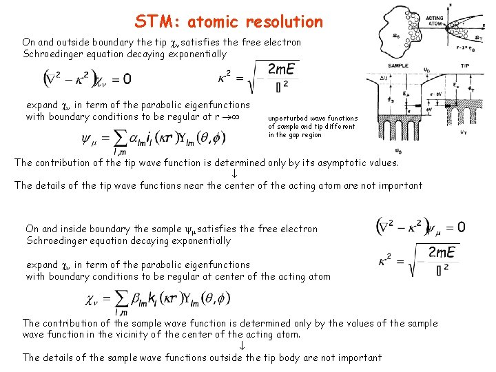
STM: atomic resolution On and outside boundary the tip satisfies the free electron Schroedinger equation decaying exponentially expand in term of the parabolic eigenfunctions with boundary conditions to be regular at r unperturbed wave functions of sample and tip different in the gap region The contribution of the tip wave function is determined only by its asymptotic values. The details of the tip wave functions near the center of the acting atom are not important On and inside boundary the sample satisfies the free electron Schroedinger equation decaying exponentially expand in term of the parabolic eigenfunctions with boundary conditions to be regular at center of the acting atom The contribution of the sample wave function is determined only by the values of the sample wave function in the vicinity of the center of the acting atom. The details of the sample wave functions outside the tip body are not important

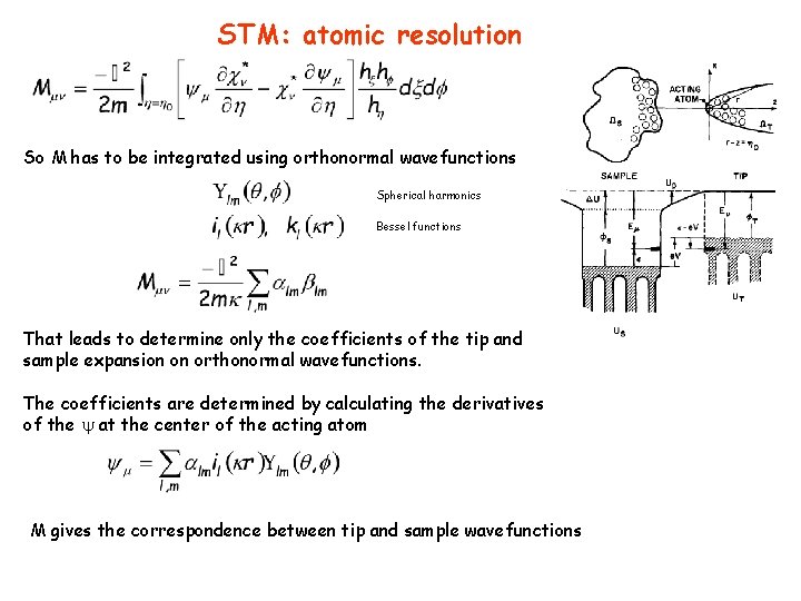
STM: atomic resolution So M has to be integrated using orthonormal wavefunctions Spherical harmonics Bessel functions That leads to determine only the coefficients of the tip and sample expansion on orthonormal wavefunctions. The coefficients are determined by calculating the derivatives of the at the center of the acting atom M gives the correspondence between tip and sample wavefunctions

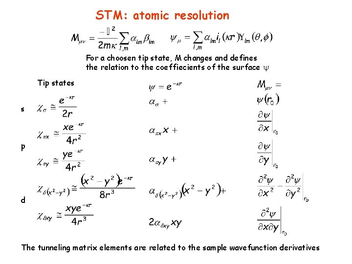
STM: atomic resolution For a choosen tip state, M changes and defines the relation to the coeffiecients of the surface Tip states s p d The tunneling matrix elements are related to the sample wavefunction derivatives

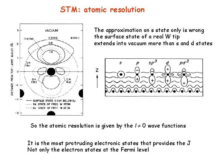
STM: atomic resolution The approximation on s state only is wrong the surface state of a real W tip extends into vacuum more than s and d states So the atomic resolution is given by the l 0 wave functions It is the most protruding electronic states that provides the J Not only the electron states at the Fermi level

STM: atomic resolution Reciprocity principle Is a basic microscopic symmetry of. STM If the "acting" electronic state of the tip and the sample state are interchanged, the image should be the same. An image of microscopic scale may be interpreted either as by probing the sample state with a tip state or by probing the tip state with a sample state

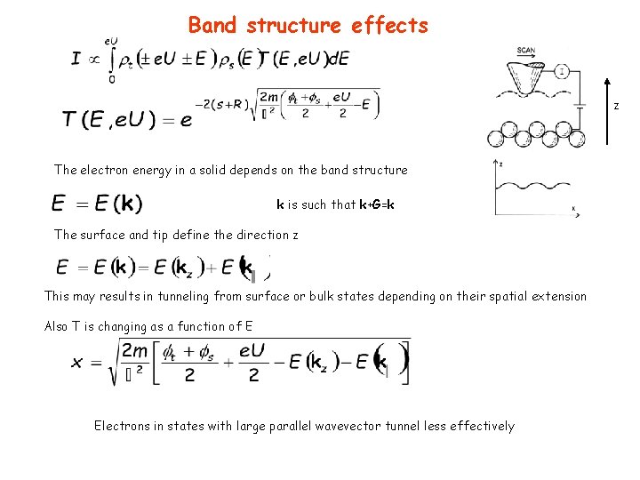
Band structure effects z The electron energy in a solid depends on the band structure k is such that k+G=k The surface and tip define the direction z This may results in tunneling from surface or bulk states depending on their spatial extension Also T is changing as a function of E Electrons in states with large parallel wavevector tunnel less effectively

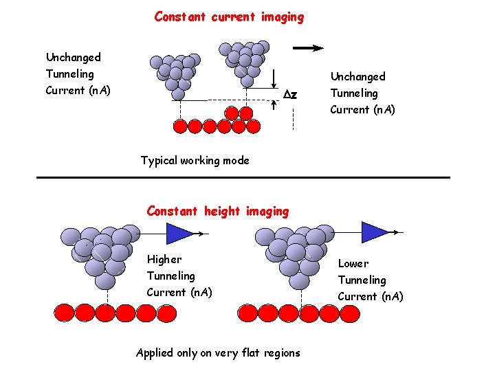
Constant current imaging Unchanged Tunneling Current (n. A) Dz Unchanged Tunneling Current (n. A) Typical working mode Constant height imaging Higher Tunneling Current (n. A) Applied only on very flat regions Lower Tunneling Current (n. A)

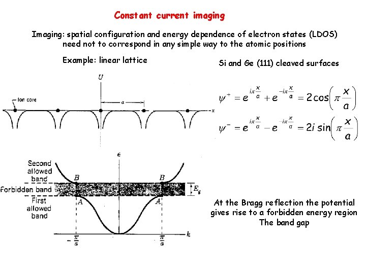
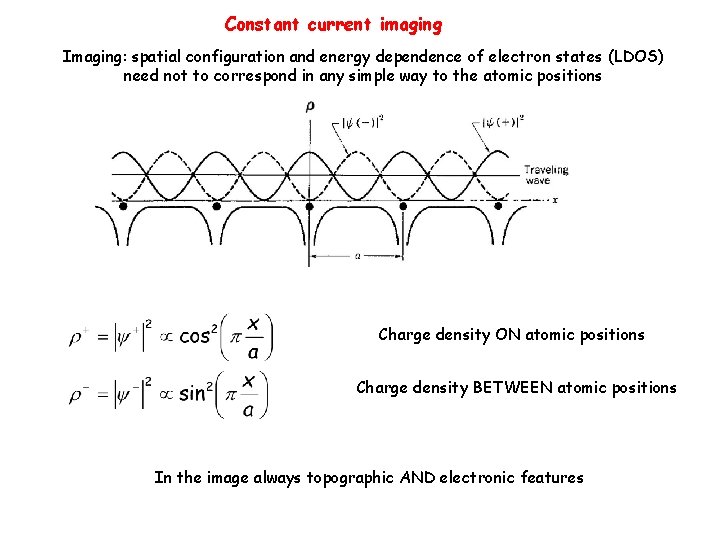
Constant current imaging Imaging: spatial configuration and energy dependence of electron states (LDOS) need not to correspond in any simple way to the atomic positions Example: linear lattice Si and Ge (111) cleaved surfaces At the Bragg reflection the potential gives rise to a forbidden energy region The band gap

Constant current imaging Imaging: spatial configuration and energy dependence of electron states (LDOS) need not to correspond in any simple way to the atomic positions Charge density ON atomic positions Charge density BETWEEN atomic positions In the image always topographic AND electronic features

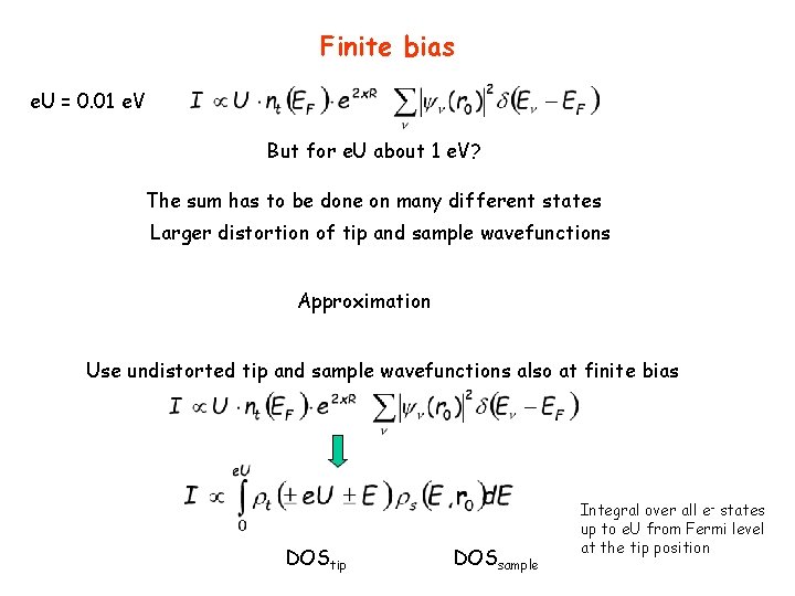
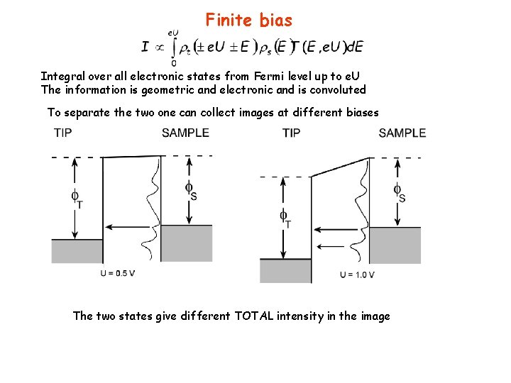
Finite bias e. U = 0. 01 e. V But for e. U about 1 e. V? The sum has to be done on many different states Larger distortion of tip and sample wavefunctions Approximation Use undistorted tip and sample wavefunctions also at finite bias DOStip DOSsample Integral over all e- states up to e. U from Fermi level at the tip position

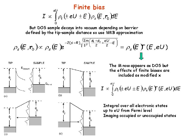
Finite bias But DOS sample decays into vacuum depending on barrier defined by the tip-sample distance so use WKB approximation The M now appears as DOS but the effects of finite biases are included as modified x Integral over all electronic states up to e. U from Fermi level Imaging occupied or unoccupied states

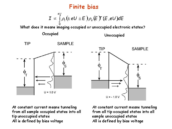
Finite bias What does it means imaging occupied or unoccupied electronic states? Occupied At constant current means tunneling from all sample occupied states into all tip unoccupied states All is defined by bias voltage Unoccupied At constant current means tunneling from all tip occupied states into all sample unoccupied states All is defined by bias voltage

Finite bias Integral over all electronic states from Fermi level up to e. U The information is geometric and electronic and is convoluted To separate the two one can collect images at different biases The two states give different TOTAL intensity in the image

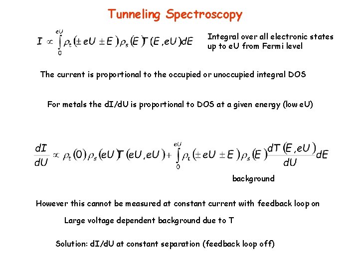
Tunneling Spectroscopy Integral over all electronic states up to e. U from Fermi level The current is proportional to the occupied or unoccupied integral DOS For metals the d. I/d. U is proportional to DOS at a given energy (low e. U) background However this cannot be measured at constant current with feedback loop on Large voltage dependent background due to T Solution: d. I/d. U at constant separation (feedback loop off)

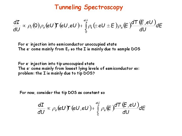
Tunneling Spectroscopy For e- injection into semiconductor unoccupied state The e- come mainly from EF so the I is mainly due to sample DOS For e- injection into tip unoccupied state The e- come mainly from lowest lying levels of semiconductor so: problem: the I is mainly due to tip DOS? For now, consider the tip DOS as constant so

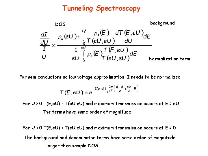
Tunneling Spectroscopy DOS background Normalization term For semiconductors no low voltage approximation: I needs to be normalized For U > 0 T(E, e. U) < T(e. U, e. U) and maximum transmission occurs at E = e. U The terms have same order of magnitude For U < 0 T(E, e. U) > T(e. U, e. U) and maximum transmission occurs at E = 0 The background and denominator terms have same order of magnitude Larger than sample DOS

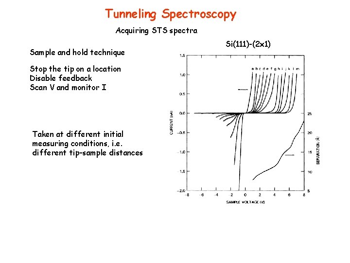
Tunneling Spectroscopy Acquiring STS spectra Sample and hold technique Stop the tip on a location Disable feedback Scan V and monitor I Taken at different initial measuring conditions, i. e. different tip-sample distances Si(111)-(2 x 1)

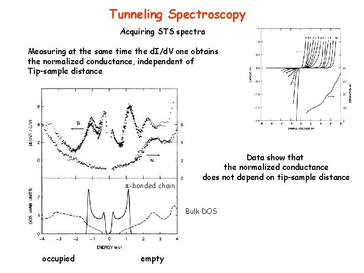
Tunneling Spectroscopy Acquiring STS spectra Measuring at the same time the d. I/d. V one obtains the normalized conductance, independent of Tip-sample distance -bonded chain Data show that the normalized conductance does not depend on tip-sample distance Bulk DOS occupied empty

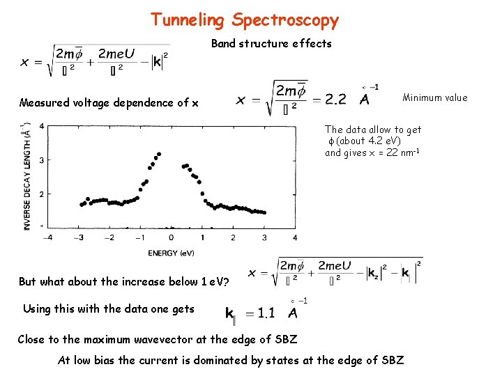
Tunneling Spectroscopy Band structure effects Measured voltage dependence of x Minimum value The data allow to get (about 4. 2 e. V) and gives x = 22 nm-1 But what about the increase below 1 e. V? Using this with the data one gets Close to the maximum wavevector at the edge of SBZ At low bias the current is dominated by states at the edge of SBZ

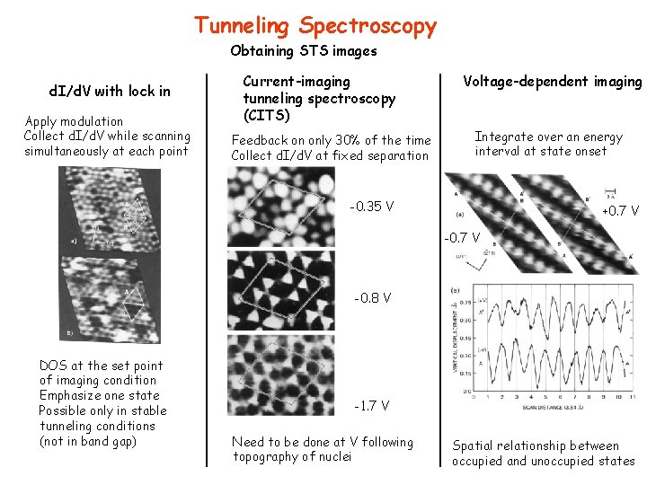
Tunneling Spectroscopy Obtaining STS images d. I/d. V with lock in Apply modulation Collect d. I/d. V while scanning simultaneously at each point Current-imaging tunneling spectroscopy (CITS) Feedback on only 30% of the time Collect d. I/d. V at fixed separation Voltage-dependent imaging Integrate over an energy interval at state onset -0. 35 V +0. 7 V -0. 8 V DOS at the set point of imaging condition Emphasize one state Possible only in stable tunneling conditions (not in band gap) -1. 7 V Need to be done at V following topography of nuclei Spatial relationship between occupied and unoccupied states

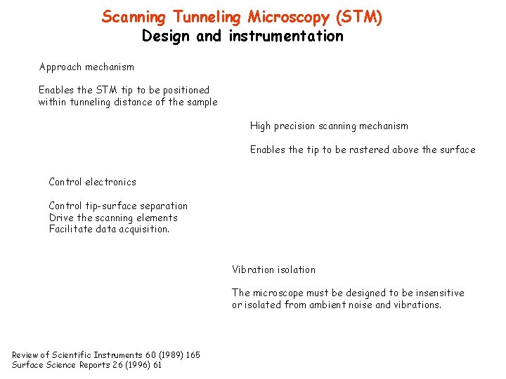
Scanning Tunneling Microscopy (STM) Design and instrumentation Approach mechanism Enables the STM tip to be positioned within tunneling distance of the sample High precision scanning mechanism Enables the tip to be rastered above the surface Control electronics Control tip-surface separation Drive the scanning elements Facilitate data acquisition. Vibration isolation The microscope must be designed to be insensitive or isolated from ambient noise and vibrations. Review of Scientific Instruments 60 (1989) 165 Surface Science Reports 26 (1996) 61

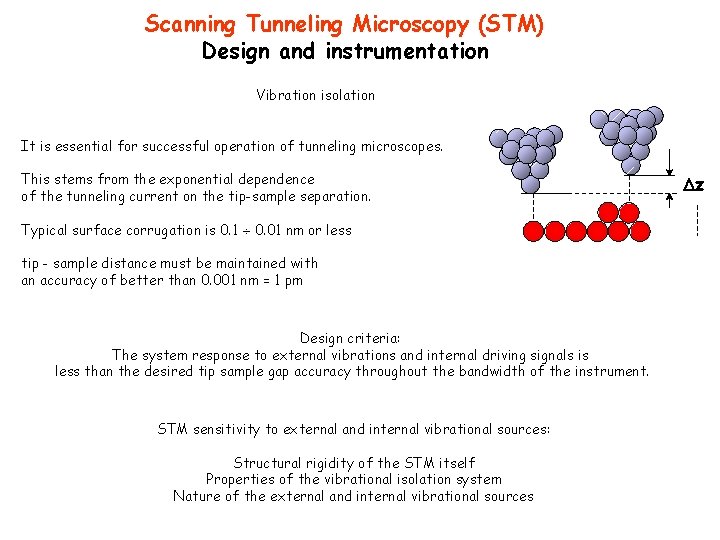
Scanning Tunneling Microscopy (STM) Design and instrumentation Vibration isolation It is essential for successful operation of tunneling microscopes. This stems from the exponential dependence of the tunneling current on the tip-sample separation. Typical surface corrugation is 0. 1 0. 01 nm or less tip - sample distance must be maintained with an accuracy of better than 0. 001 nm = 1 pm Design criteria: The system response to external vibrations and internal driving signals is less than the desired tip sample gap accuracy throughout the bandwidth of the instrument. STM sensitivity to external and internal vibrational sources: Structural rigidity of the STM itself Properties of the vibrational isolation system Nature of the external and internal vibrational sources Dz

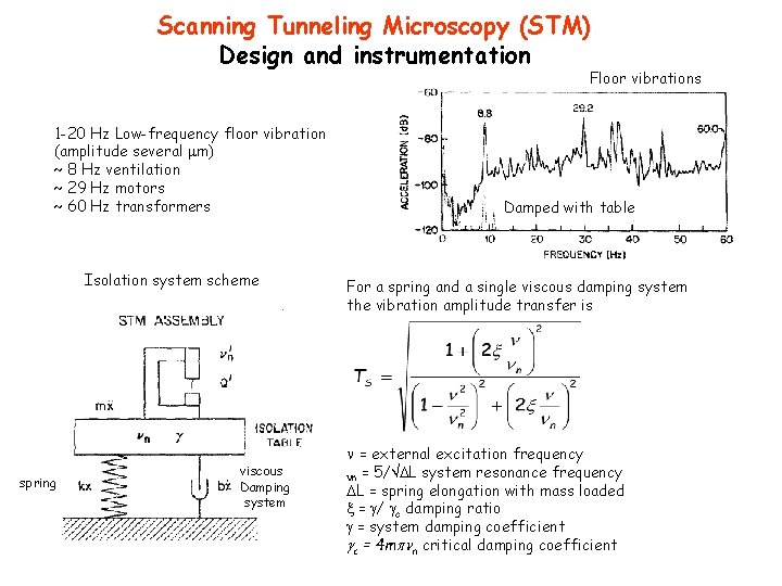
Scanning Tunneling Microscopy (STM) Design and instrumentation Floor vibrations 1 -20 Hz Low-frequency floor vibration (amplitude several m) ~ 8 Hz ventilation ~ 29 Hz motors ~ 60 Hz transformers Isolation system scheme spring viscous Damping system Damped with table For a spring and a single viscous damping system the vibration amplitude transfer is = external excitation frequency n = 5/ L system resonance frequency L = spring elongation with mass loaded = / c damping ratio = system damping coefficient c = 4 m n critical damping coefficient

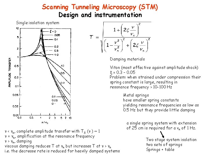
Scanning Tunneling Microscopy (STM) Design and instrumentation Single isolation system Damping materials Viton (most effective against amplitude shock) = 0. 3 – 0. 05 Problem: when strained under compression their spring constant is large, resulting in resonance frequency > 10 -100 Hz Metal springs have smaller spring constants yielding resonance frequencies as low as 0. 5 Hz but they provide little damping < n, complete amplitude transfer with TS ( ) ~ 1 = n, amplification at the resonance frequency > n, damping viscous damping reduces T at n but increases T at > n i. e. the decrease rate is reduced for heavily damped systems a single spring system with extension of 25 cm is required for a vn of 1 Hz. Two stage system isolation two sets of springs Springs + table

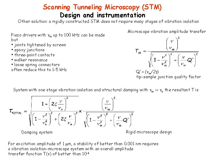
Scanning Tunneling Microscopy (STM) Design and instrumentation Other solution: a rigidly constructed STM does not require many stages of vibration isolation Piezo drivers with m up to 100 k. Hz can be made but • joints tightened by screws • epoxy junctions • three-point contacts • walker resonance • loose spring connectors often reduce this to 1 -5 k. Hz Microscope vibration amplitude transfer Q’ = ( m/2 ) tip-sample junction quality factor System with one stage vibration isolation and structural damping with m >> n the resultant T is Damping system Rigid microscope design For excitation amplitude of 1 m, a stability of better than 0. 001 nm requires a vibration isolation-microscope system with an overall amplitude transfer function T( ) of better than 10 -6

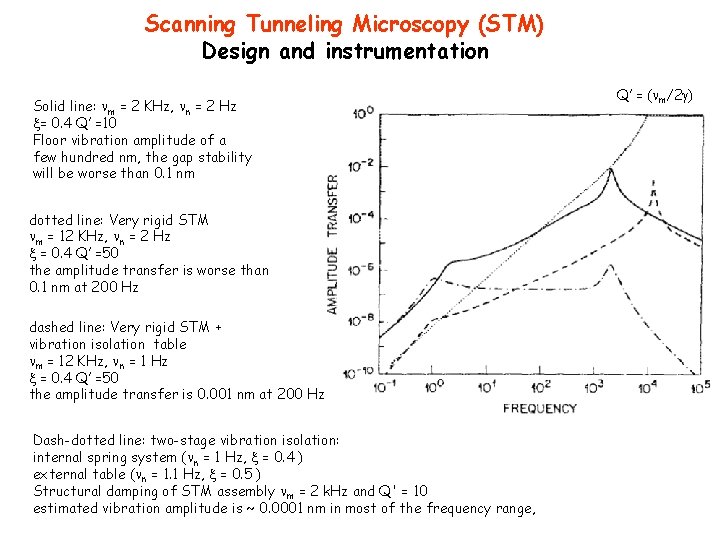
Scanning Tunneling Microscopy (STM) Design and instrumentation Solid line: m = 2 KHz, n = 2 Hz = 0. 4 Q’ =10 Floor vibration amplitude of a few hundred nm, the gap stability will be worse than 0. 1 nm dotted line: Very rigid STM m = 12 KHz, n = 2 Hz = 0. 4 Q’ =50 the amplitude transfer is worse than 0. 1 nm at 200 Hz dashed line: Very rigid STM + vibration isolation table m = 12 KHz, n = 1 Hz = 0. 4 Q’ =50 the amplitude transfer is 0. 001 nm at 200 Hz Dash-dotted line: two-stage vibration isolation: internal spring system ( n = 1 Hz, = 0. 4 ) external table ( n = 1. 1 Hz, = 0. 5 ) Structural damping of STM assembly m = 2 k. Hz and Q' = 10 estimated vibration amplitude is ~ 0. 0001 nm in most of the frequency range, Q’ = ( m/2 )

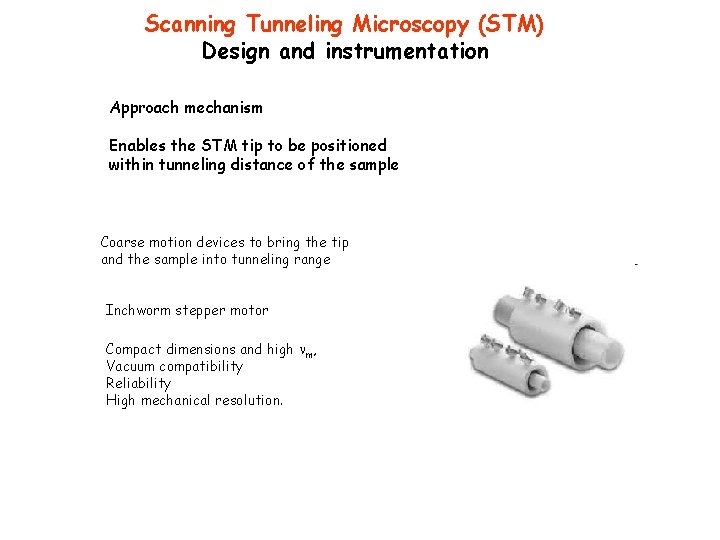
Scanning Tunneling Microscopy (STM) Design and instrumentation Approach mechanism Enables the STM tip to be positioned within tunneling distance of the sample Coarse motion devices to bring the tip and the sample into tunneling range Inchworm stepper motor Compact dimensions and high m, Vacuum compatibility Reliability High mechanical resolution.

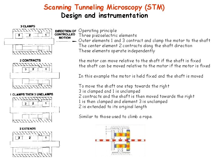
Scanning Tunneling Microscopy (STM) Design and instrumentation Operating principle Three piezoelectric elements Outer elements 1 and 3 contract and clamp the motor to the shaft The center element 2 contracts along the shaft direction These elements operate independently the motor can move relative to the shaft if the shaft is fixed the shaft can be moved relative to the motor if the motor is fixed In this example the motor is held fixed and the shaft is moved To move the shaft one step towards the right 3 is clamped and 1 is unclamped 2 contracts and the shaft is then moved towards the right 1 is then clamped and element 3 is unclamped 2 is extended to its original length Similar to those used to climb a rope.

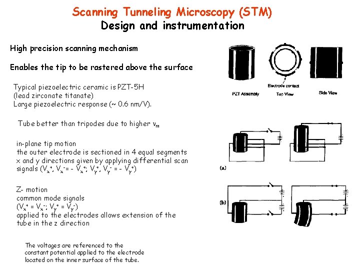
Scanning Tunneling Microscopy (STM) Design and instrumentation High precision scanning mechanism Enables the tip to be rastered above the surface Typical piezoelectric ceramic is PZT-5 H (lead zirconate titanate) Large piezoelectric response (~ 0. 6 nm/V). Tube better than tripodes due to higher m in-plane tip motion the outer electrode is sectioned in 4 equal segments x and y directions given by applying differential scan signals (Vx+, Vx-= - Vx+; Vy+, Vy- = - Vy+) Z- motion common mode signals (Vx+ = Vx-; Vy+ = Vy-) applied to the electrodes allows extension of the tube in the z direction The voltages are referenced to the constant potential applied to the electrode located on the inner surface of the tube.

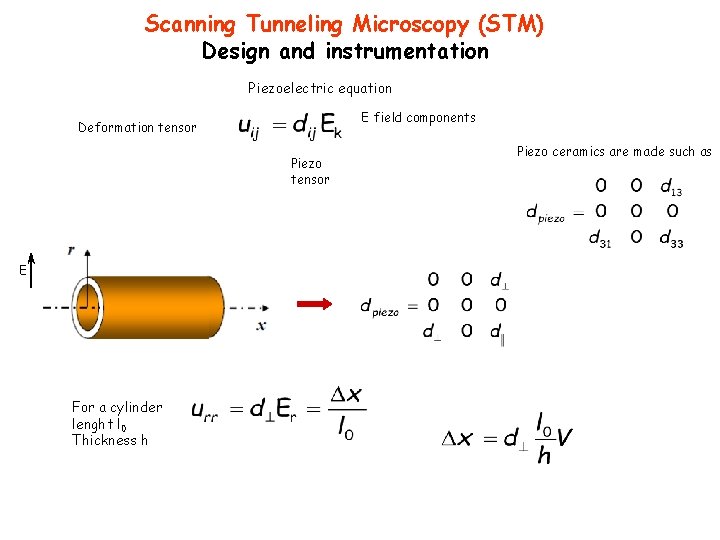
Scanning Tunneling Microscopy (STM) Design and instrumentation Piezoelectric equation E field components Deformation tensor Piezo tensor E For a cylinder lenght l 0 Thickness h Piezo ceramics are made such as

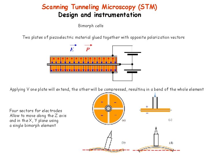
Scanning Tunneling Microscopy (STM) Design and instrumentation Bimorph cells Two plates of piezoelectric material glued together with opposite polarization vectors Applying V one plate will extend, the other will be compressed, resulting in a bend of the whole element Four sectors for electrodes Allow to move along the Z axis and in the X, Y plane using a single bimorph element

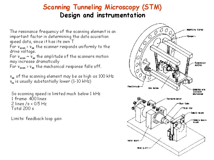
Scanning Tunneling Microscopy (STM) Design and instrumentation The resonance frequency of the scanning element is an important factor in determining the data acuisition speed data, since it has its own T For scan < se the scanner responds uniformly to the drive voltage. For scan ~ se the amplitude of the scanners motion may increase dramatically For scan > se the mechanical response falls off. se of the scanning element may be as high as 100 k. Hz m is usually substantially lower (1 -10 k. Hz) So scanning speed is limited much below 1 k. Hz 1 frame: 400 lines 2 lines /s = 0. 5 Hz Total 200 s Limits: feedback loop gain

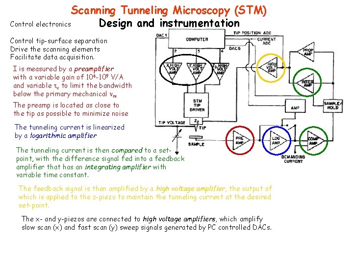
Scanning Tunneling Microscopy (STM) Control electronics Design and instrumentation Control tip-surface separation Drive the scanning elements Facilitate data acquisition. I is measured by a preamplifier with a variable gain of 106 -109 V/A and variable c to limit the bandwidth below the primary mechanical m The preamp is located as close to the tip as possible to minimize noise The tunneling current is linearized by a logarithmic amplifier The tunneling current is then compared to a setpoint, with the difference signal fed into a feedback amplifier that has an integrating amplifier with variable time constant. The feedback signal is then amplified by a high voltage amplifier, the output of which is applied to the z-piezo to maintain the tunneling current at the desired set-point. The x- and y-piezos are connected to high voltage amplifiers, which amplify slow scan (x) and fast scan (y) sweep signals generated by PC controlled DACs.

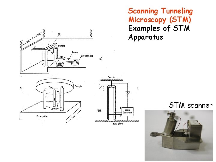
Scanning Tunneling Microscopy (STM) Examples of STM Apparatus STM scanner

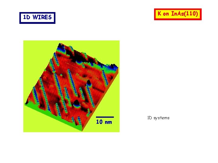
K on In. As(110) 1 D WIRES 10 nm 1 D systems

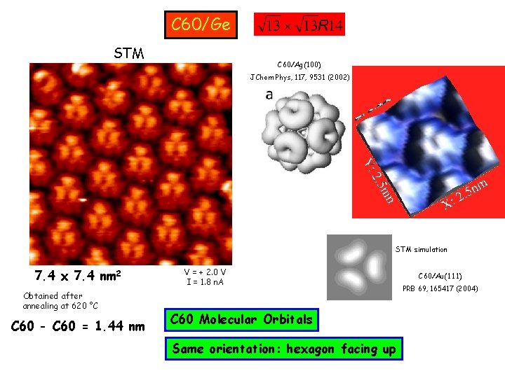
C 60/Ge STM C 60/Ag(100) J Chem Phys, 117, 9531 (2002) STM simulation 7. 4 x 7. 4 nm 2 Obtained after annealing at 620 °C C 60 - C 60 = 1. 44 nm V = + 2. 0 V I = 1. 8 n. A C 60 Molecular Orbitals Same orientation: hexagon facing up C 60/Au(111) PRB 69, 165417 (2004)

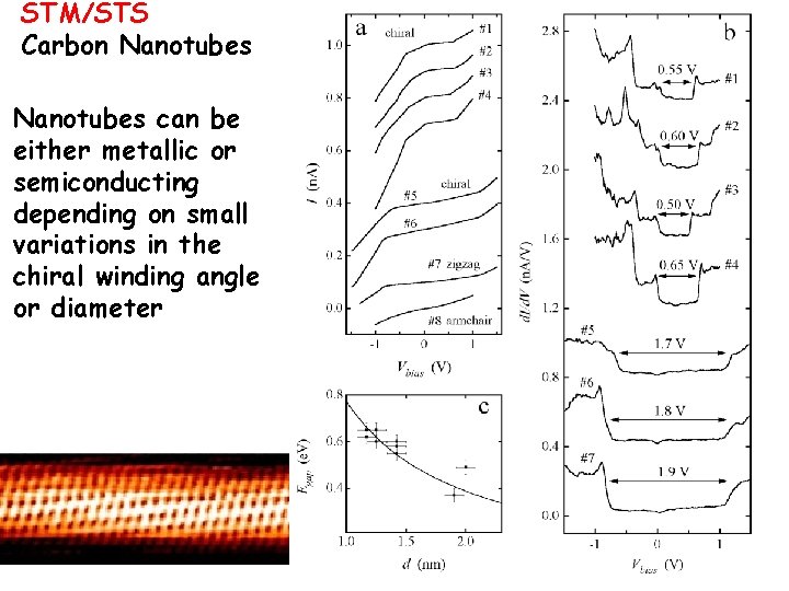
STM/STS Carbon Nanotubes can be either metallic or semiconducting depending on small variations in the chiral winding angle or diameter

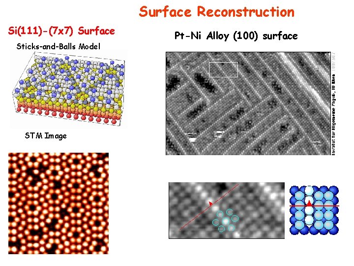
Surface Reconstruction Si(111)-(7 x 7) Surface Sticks-and-Balls Model STM Image Pt-Ni Alloy (100) surface

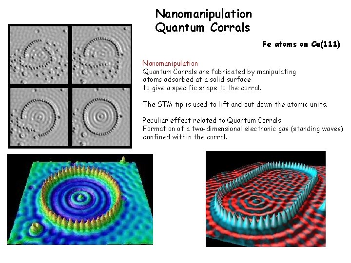
Nanomanipulation Quantum Corrals Fe atoms on Cu(111) Nanomanipulation Quantum Corrals are fabricated by manipulating atoms adsorbed at a solid surface to give a specific shape to the corral. The STM tip is used to lift and put down the atomic units. Peculiar effect related to Quantum Corrals Formation of a two-dimensional electronic gas (standing waves) confined within the corral.

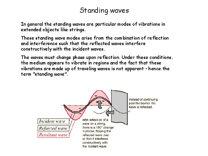
Standing waves In general the standing waves are particular modes of vibrations in extended objects like strings. These standing wave modes arise from the combination of reflection and interference such that the reflected waves interfere constructively with the incident waves. The waves must change phase upon reflection. Under these conditions, the medium appears to vibrate in regions and the fact that these vibrations are made up of traveling waves is not apparent - hence the term "standing wave".

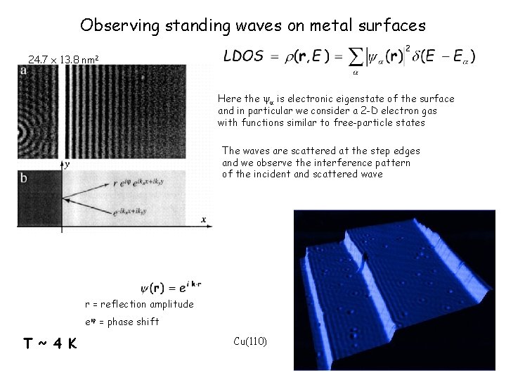
Observing standing waves on metal surfaces 24. 7 x 13. 8 nm 2 Here the is electronic eigenstate of the surface and in particular we consider a 2 -D electron gas with functions similar to free-particle states The waves are scattered at the step edges and we observe the interference pattern of the incident and scattered wave r = reflection amplitude ei = phase shift T ~ 4 K Cu(110)

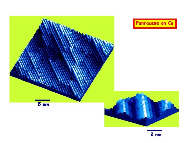
Pentacene on Cu 5 nm 2 nm

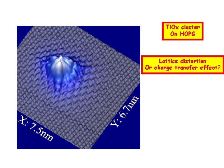
Ti. Ox cluster On HOPG Lattice distortion Or charge transfer effect?

Cu on Cu(111) Instability And Diffusion coefficient 150 x 150 nm 2

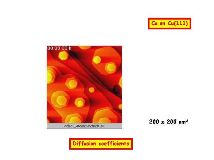
Cu on Cu(111) 200 x 200 nm 2 Diffusion coefficients

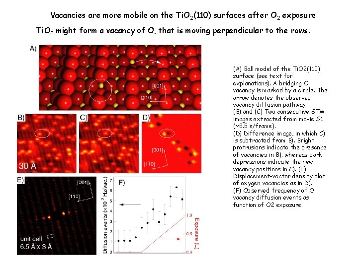
Vacancies are mobile on the Ti. O 2(110) surfaces after O 2 exposure Ti. O 2 might form a vacancy of O, that is moving perpendicular to the rows. (A) Ball model of the Ti. O 2(110) surface (see text for explanations). A bridging O vacancy is marked by a circle. The arrow denotes the observed vacancy diffusion pathway. (B) and (C) Two consecutive STM images extracted from movie S 1 (~8. 5 s/frame). (D) Difference image, in which C) is subtracted from B). Bright protrusions indicate the presence of vacancies in B), whereas dark depressions indicate the new vacancy positions in C). (E) Displacement-vector density plot of oxygen vacancies as in D). (F) Observed frequency of O vacancy diffusion events as function of O 2 exposure.

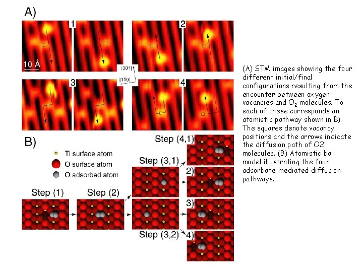
(A) STM images showing the four different initial/final configurations resulting from the encounter between oxygen vacancies and O 2 molecules. To each of these corresponds an atomistic pathway shown in B). The squares denote vacancy positions and the arrows indicate the diffusion path of O 2 molecules. (B) Atomistic ball model illustrating the four adsorbate-mediated diffusion pathways.

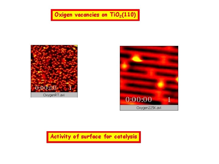
Oxigen vacancies on Ti. O 2(110) Activity of surface for catalysis

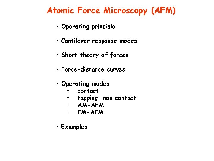
Atomic Force Microscopy (AFM) • Operating principle • Cantilever response modes • Short theory of forces • Force-distance curves • Operating modes • contact • tapping –non contact • AM-AFM • FM-AFM • Examples

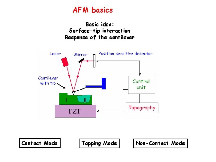
AFM basics Basic idea: Surface-tip interaction Response of the cantilever Contact Mode Tapping Mode Non-Contact Mode

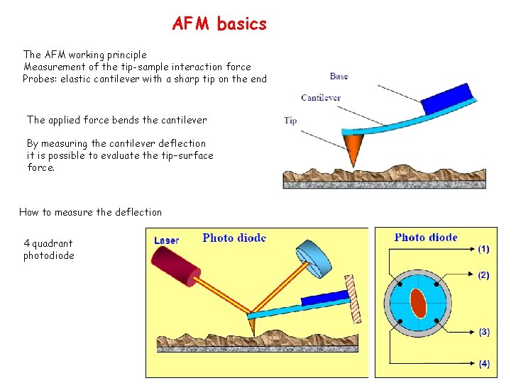
AFM basics The AFM working principle Measurement of the tip-sample interaction force Probes: elastic cantilever with a sharp tip on the end The applied force bends the cantilever By measuring the cantilever deflection it is possible to evaluate the tip–surface force. How to measure the deflection 4 quadrant photodiode

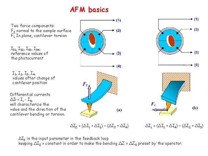
AFM basics Two force components: FZ normal to the sample surface FL In plane, cantilever torsion I 01, I 02, I 03, I 04, reference values of the photocurrent I 1, I 2, I 3, I 4, values after change of cantilever position Differential currents ΔIi = Ii - I 0 i will characterize the value and the direction of the cantilever bending or torsion. ΔIZ = (ΔI 1 + ΔI 2) − (ΔI 3 + ΔI 4) ΔIL = (ΔI 1 + ΔI 4) − (ΔI 2 + ΔI 3) ΔIZ is the input parameter in the feedback loop keeping ΔIZ = constant in order to make the bending ΔZ = ΔZ 0 preset by the operator.

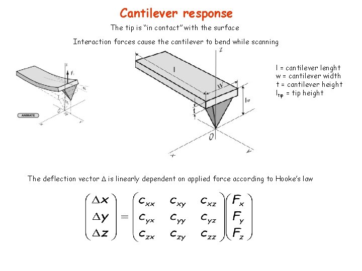
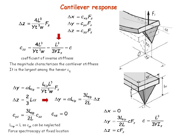
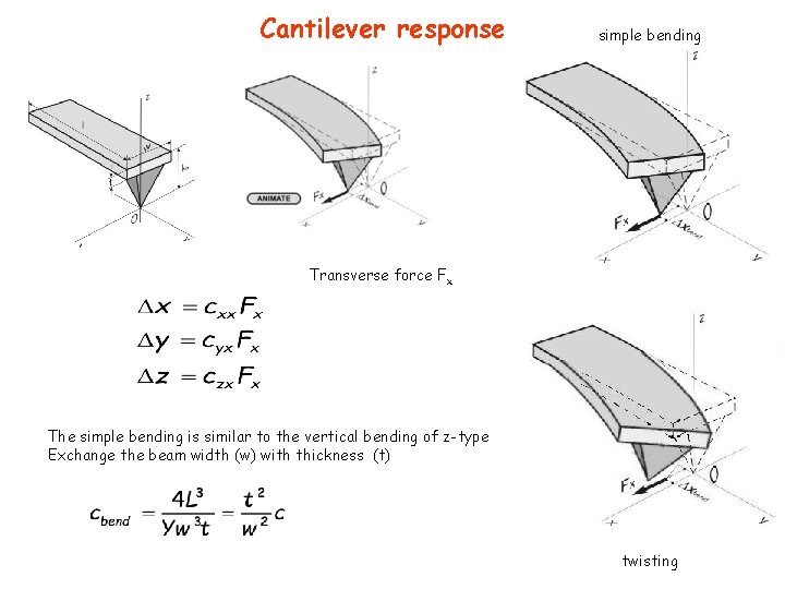
Cantilever response The tip is “in contact” with the surface Interaction forces cause the cantilever to bend while scanning l = cantilever lenght w = cantilever width t = cantilever height ltip = tip height The deflection vector is linearly dependent on applied force according to Hooke’s law

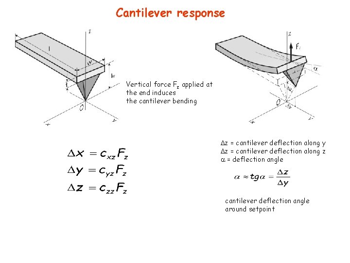
Cantilever response Vertical force Fz applied at the end induces the cantilever bending z = cantilever deflection along y z = cantilever deflection along z = deflection angle cantilever deflection angle around setpoint

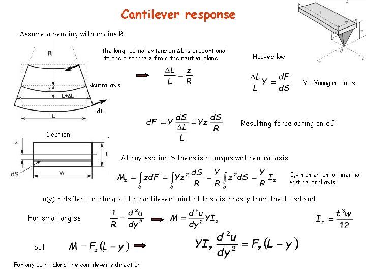
Cantilever response Assume a bending with radius R the longitudinal extension L is proportional to the distance z from the neutral plane Hooke’s law Y = Young modulus Neutral axis d. F Resulting force acting on d. S Section At any section S there is a torque wrt neutral axis Iz= momentum of inertia wrt neutral axis u(y) = deflection along z of a cantilever point at the distance y from the fixed end For small angles but For any point along the cantilever y direction

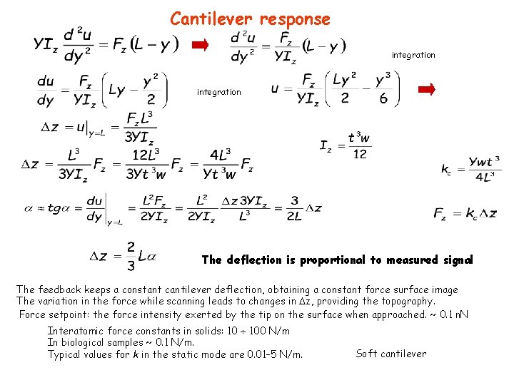
Cantilever response integration The deflection is proportional to measured signal The feedback keeps a constant cantilever deflection, obtaining a constant force surface image The variation in the force while scanning leads to changes in z, providing the topography. Force setpoint: the force intensity exerted by the tip on the surface when approached. ~ 0. 1 n. N Interatomic force constants in solids: 10 100 N/m In biological samples ~ 0. 1 N/m. Typical values for k in the static mode are 0. 01– 5 N/m. Soft cantilever

Cantilever response coefficient of inverse stiffness The magnitude characterizes the cantilever stiffness It is the largest among the tensor cij Ltip << L so cyz can be neglected Force spectroscopy at fixed location

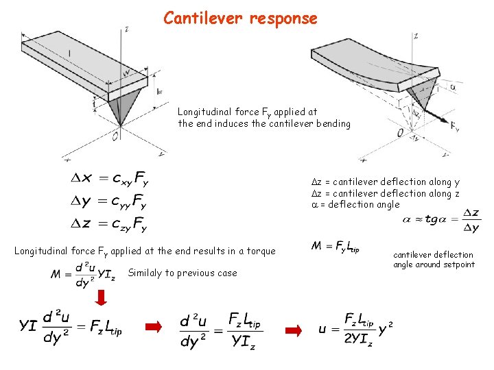
Cantilever response Longitudinal force Fy applied at the end induces the cantilever bending z = cantilever deflection along y z = cantilever deflection along z = deflection angle Longitudinal force Fy applied at the end results in a torque Similaly to previous case cantilever deflection angle around setpoint

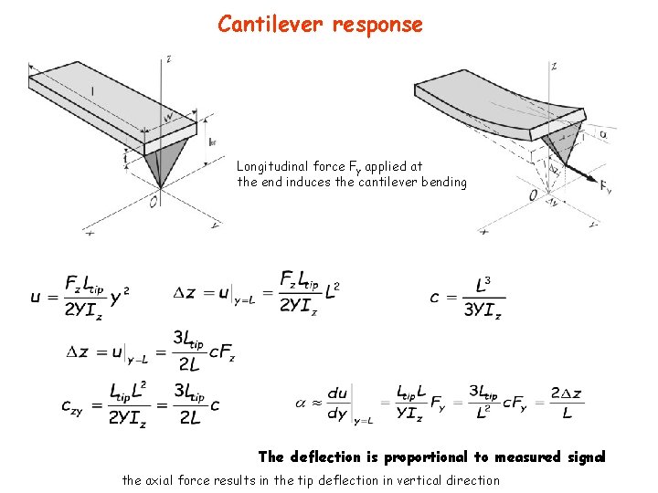
Cantilever response Longitudinal force Fy applied at the end induces the cantilever bending The deflection is proportional to measured signal the axial force results in the tip deflection in vertical direction

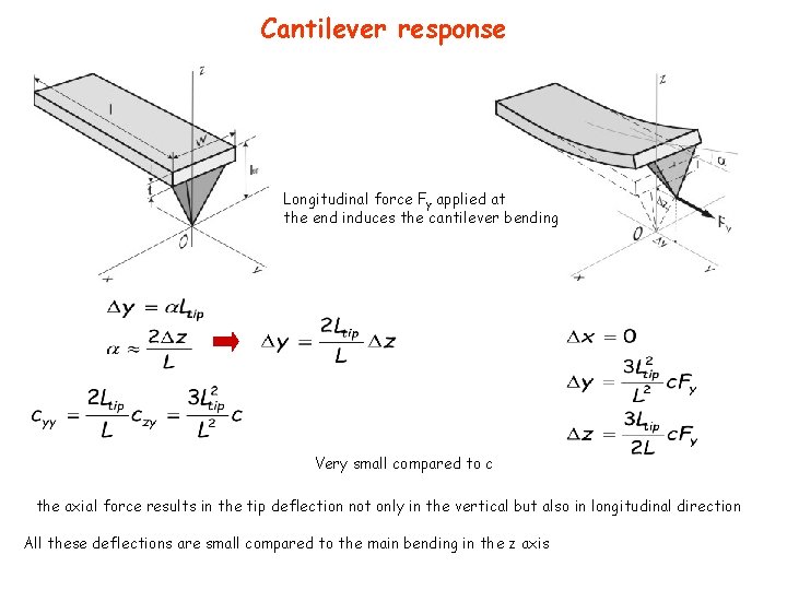
Cantilever response Longitudinal force Fy applied at the end induces the cantilever bending Very small compared to c the axial force results in the tip deflection not only in the vertical but also in longitudinal direction All these deflections are small compared to the main bending in the z axis

Cantilever response simple bending Transverse force Fx The simple bending is similar to the vertical bending of z-type Exchange the beam width (w) with thickness (t) twisting

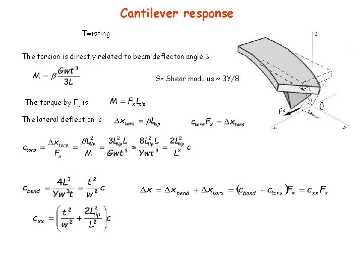
Cantilever response Twisting The torsion is directly related to beam deflecton angle G= Shear modulus ~ 3 Y/8 The torque by Fx is The lateral deflection is

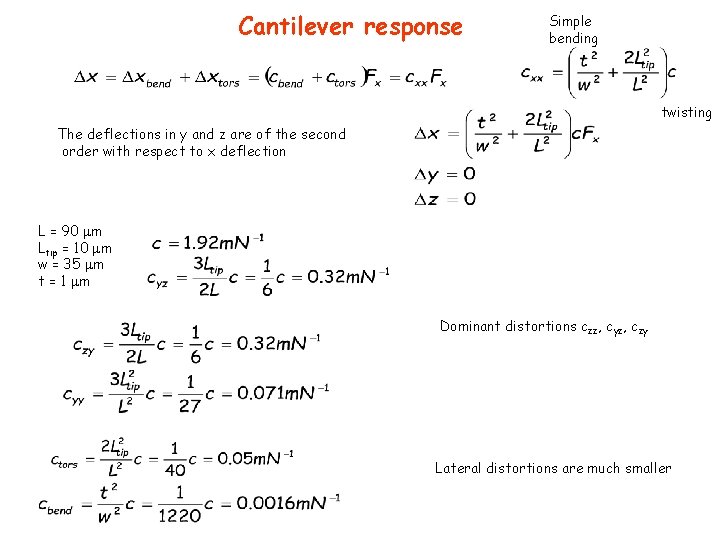
Cantilever response Simple bending twisting The deflections in y and z are of the second order with respect to x deflection L = 90 m Ltip = 10 m w = 35 m t = 1 m Dominant distortions czz, cyz, czy Lateral distortions are much smaller

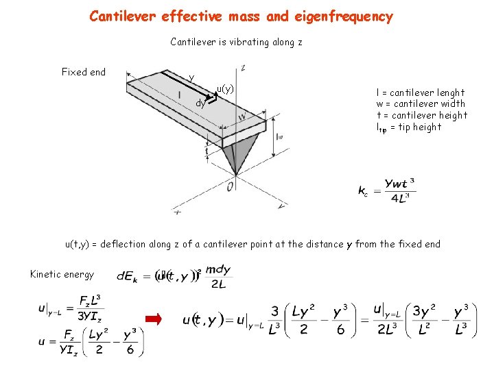
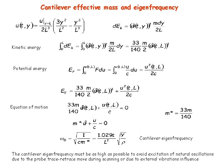
Cantilever effective mass and eigenfrequency Cantilever is vibrating along z Fixed end y u(y) dy l = cantilever lenght w = cantilever width t = cantilever height ltip = tip height u(t, y) = deflection along z of a cantilever point at the distance y from the fixed end Kinetic energy

Cantilever effective mass and eigenfrequency Kinetic energy Potential energy Equation of motion Cantilever eigenfrequency The cantilever eigenfrequency must be as high as possible to avoid excitation of natural oscillations due to the probe trace-retrace move during scanning or due to external vibrations influence

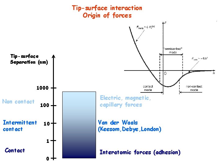
Tip-surface interaction Origin of forces Tip-surface Separation (nm) 1000 Non contact Intermittent contact 100 10 Electric, magnetic, capillary forces Van der Waals (Keesom, Debye, London) 1 Contact 0 Interatomic forces (adhesion)

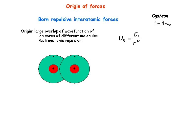
Origin of forces Born repulsive interatomic forces Origin: large overlap of wavefunction of ion cores of different molecules Pauli and ionic repulsion - - + + Cgs/esu

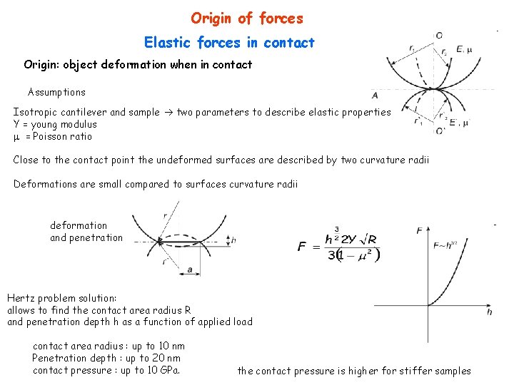
Origin of forces Elastic forces in contact Origin: object deformation when in contact Assumptions Isotropic cantilever and sample two parameters to describe elastic properties Y = young modulus = Poisson ratio Close to the contact point the undeformed surfaces are described by two curvature radii Deformations are small compared to surfaces curvature radii deformation and penetration Hertz problem solution: allows to find the contact area radius R and penetration depth h as a function of applied load contact area radius : up to 10 nm Penetration depth : up to 20 nm contact pressure : up to 10 GPa. the contact pressure is higher for stiffer samples

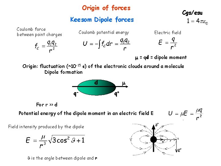
Origin of forces Cgs/esu Keesom Dipole forces Coulomb force between point charges Coulomb potential energy Electric field = qd = dipole moment Origin: fluctuation (~10 -15 s) of the electronic clouds around a molecule Dipole formation d q- q+ For r >> d Potential energy of the dipole moment in an electric field E Field intensity produced by the dipole is the angle between dipole and r

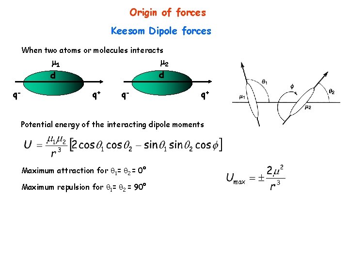
Origin of forces Keesom Dipole forces When two atoms or molecules interacts 2 1 d d q- q+ Potential energy of the interacting dipole moments Maximum attraction for 1= 2 = 0° Maximum repulsion for 1= 2 = 90°

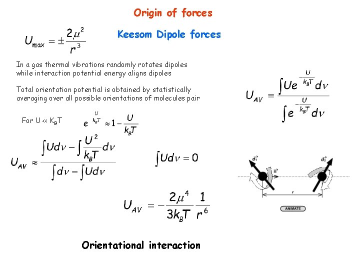
Origin of forces Keesom Dipole forces In a gas thermal vibrations randomly rotates dipoles while interaction potential energy aligns dipoles Total orientation potential is obtained by statistically averaging over all possible orientations of molecules pair For U << KBT Orientational interaction

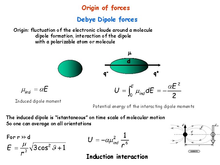
Origin of forces Debye Dipole forces Origin: fluctuation of the electronic clouds around a molecule dipole formation, interaction of the dipole with a polarizable atom or molecule d q- Induced dipole moment q+ Potential energy of the interacting dipole moments The induced dipole is “istantaneous” on time scale of molecular motion So one can average on all orientations For r >> d Induction interaction

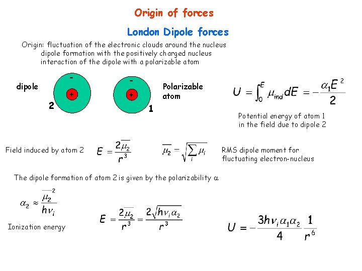
Origin of forces London Dipole forces Origin: fluctuation of the electronic clouds around the nucleus dipole formation with the positively charged nucleus interaction of the dipole with a polarizable atom dipole 2 - - + + Polarizable atom 1 Field induced by atom 2 The dipole formation of atom 2 is given by the polarizability Ionization energy Potential energy of atom 1 in the field due to dipole 2 RMS dipole moment for fluctuating electron-nucleus

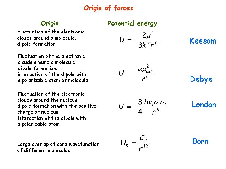
Origin of forces Origin Potential energy Fluctuation of the electronic clouds around a molecule. dipole formation Keesom Fluctuation of the electronic clouds around a molecule. dipole formation. interaction of the dipole with a polarizable atom or molecule Debye Fluctuation of the electronic clouds around the nucleus. dipole formation with the positive charge of nucleus. interaction of the dipole with a polarizable atom Large overlap of core wavefunction of different molecules London Born

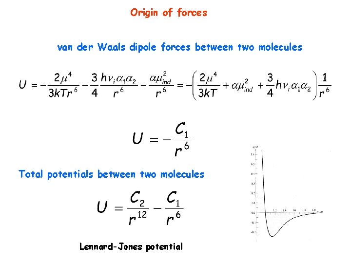
Origin of forces van der Waals dipole forces between two molecules Total potentials between two molecules Lennard-Jones potential

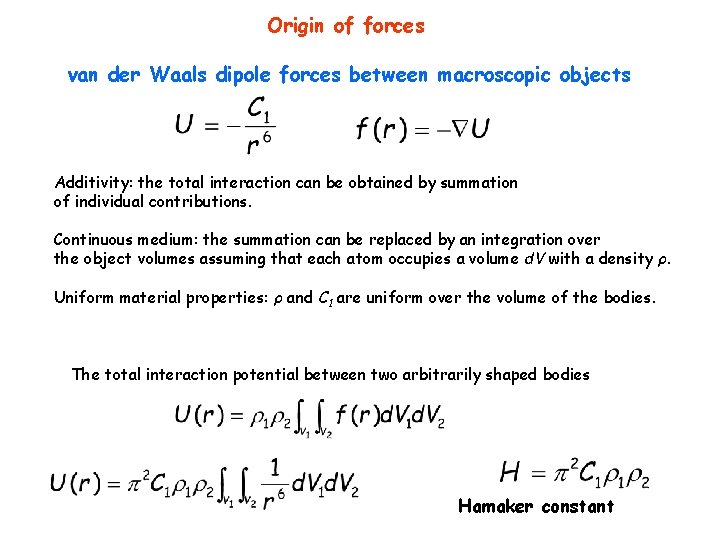
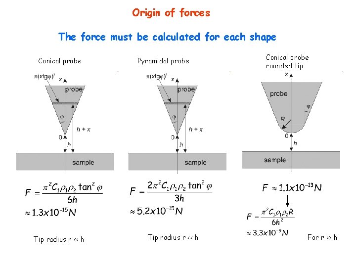
Origin of forces van der Waals dipole forces between macroscopic objects Additivity: the total interaction can be obtained by summation of individual contributions. Continuous medium: the summation can be replaced by an integration over the object volumes assuming that each atom occupies a volume d. V with a density ρ. Uniform material properties: ρ and C 1 are uniform over the volume of the bodies. The total interaction potential between two arbitrarily shaped bodies Hamaker constant

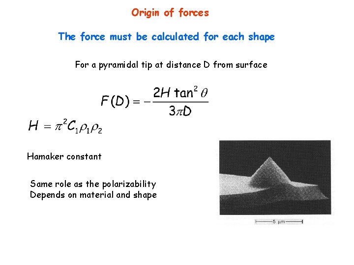
Origin of forces The force must be calculated for each shape For a pyramidal tip at distance D from surface Hamaker constant Same role as the polarizability Depends on material and shape

Origin of forces The force must be calculated for each shape Conical probe Tip radius r << h Pyramidal probe Tip radius r << h Conical probe rounded tip For r >> h

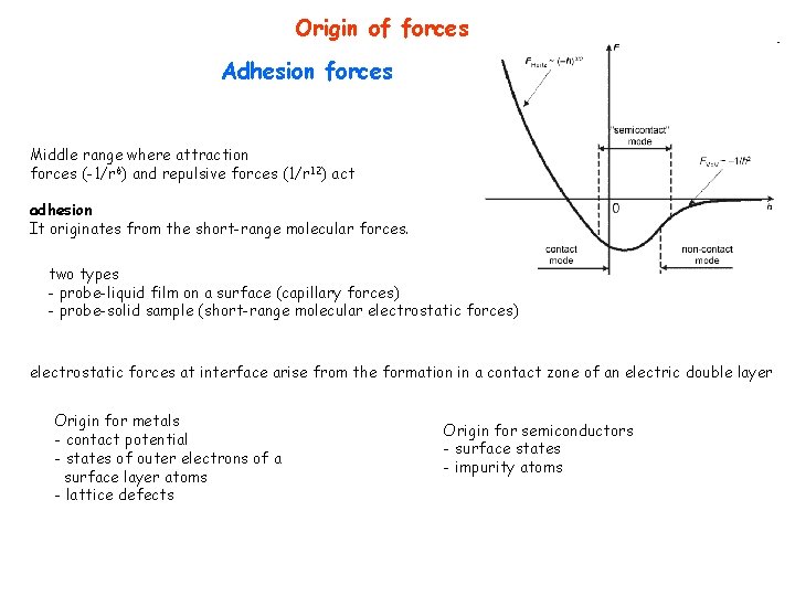
Origin of forces Adhesion forces Middle range where attraction forces (-1/r 6) and repulsive forces (1/r 12) act adhesion It originates from the short-range molecular forces. two types - probe-liquid film on a surface (capillary forces) - probe-solid sample (short-range molecular electrostatic forces) electrostatic forces at interface arise from the formation in a contact zone of an electric double layer Origin for metals - contact potential - states of outer electrons of a surface layer atoms - lattice defects Origin for semiconductors - surface states - impurity atoms

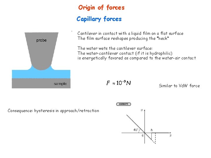
Origin of forces Capillary forces Cantilever in contact with a liquid film on a flat surface The film surface reshapes producing the "neck“ The water wets the cantilever surface: The water-cantilever contact (if it is hydrophilic) is energetically favored as compared to the water-air contact Similar to Vd. W force Consequence: hysteresis in approach/retraction

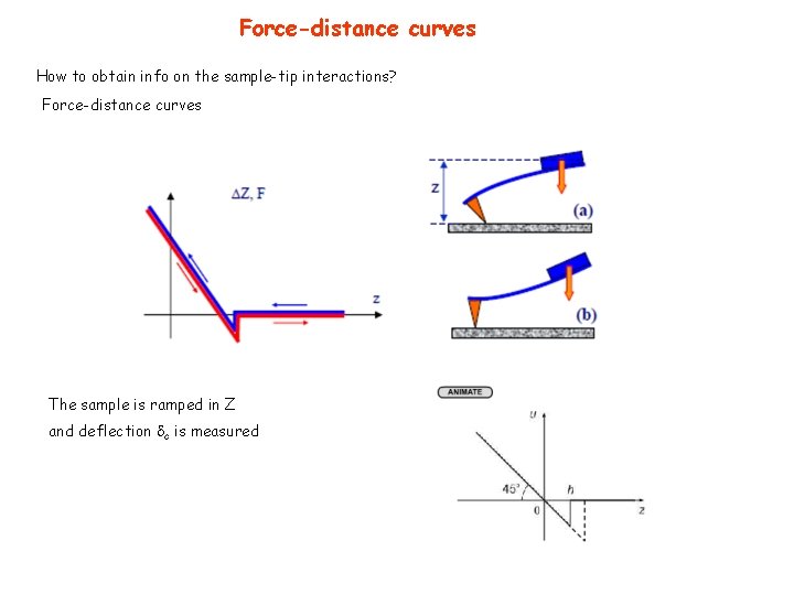
Force-distance curves How to obtain info on the sample-tip interactions? Force-distance curves The sample is ramped in Z and deflection c is measured

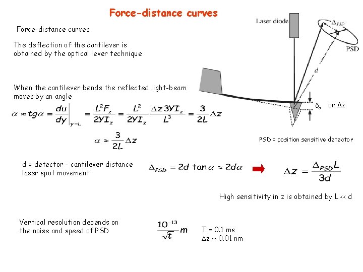
Force-distance curves The deflection of the cantilever is obtained by the optical lever technique When the cantilever bends the reflected light-beam moves by an angle c or z PSD = position sensitive detector d = detector - cantilever distance laser spot movement High sensitivity in z is obtained by L << d Vertical resolution depends on the noise and speed of PSD T = 0. 1 ms z ~ 0. 01 nm

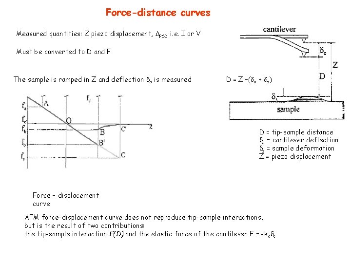
Force-distance curves Measured quantities: Z piezo displacement, PSD i. e. I or V Must be converted to D and F The sample is ramped in Z and deflection c is measured D = Z –( c + s) D = tip-sample distance c = cantilever deflection s = sample deformation Z = piezo displacement Force – displacement curve AFM force-displacement curve does not reproduce tip-sample interactions, but is the result of two contributions: the tip-sample interaction F(D) and the elastic force of the cantilever F = -kc c

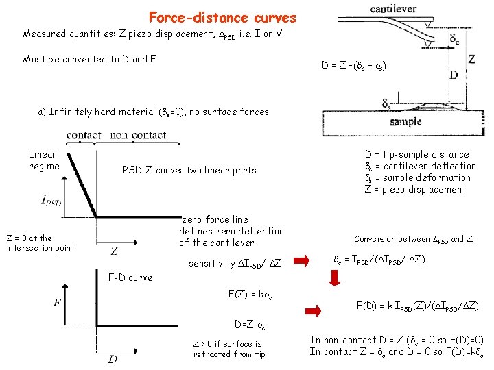
Force-distance curves Measured quantities: Z piezo displacement, PSD i. e. I or V Must be converted to D and F D = Z –( c + s) a) Infinitely hard material ( s=0), no surface forces Linear regime PSD-Z curve: two linear parts zero force line defines zero deflection of the cantilever Z = 0 at the intersection point F-D curve sensitivity IPSD/ Z F(Z) = k c D = tip-sample distance c = cantilever deflection s = sample deformation Z = piezo displacement Conversion between PSD and Z c = IPSD/( IPSD/ Z) F(D) = k IPSD(Z)/( IPSD/ Z) D=Z- c Z > 0 if surface is retracted from tip In non-contact D = Z ( c = 0 so F(D)=0) In contact Z = c and D = 0 so F(D)=k c

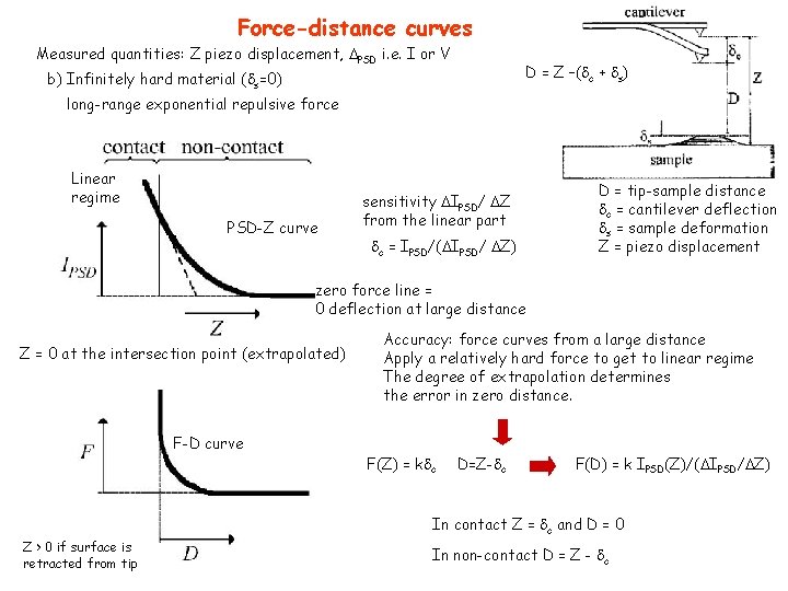
Force-distance curves Measured quantities: Z piezo displacement, PSD i. e. I or V D = Z –( c + s) b) Infinitely hard material ( s=0) long-range exponential repulsive force Linear regime PSD-Z curve sensitivity IPSD/ Z from the linear part c = IPSD/( IPSD/ Z) D = tip-sample distance c = cantilever deflection s = sample deformation Z = piezo displacement zero force line = 0 deflection at large distance Z = 0 at the intersection point (extrapolated) F-D curve Accuracy: force curves from a large distance Apply a relatively hard force to get to linear regime The degree of extrapolation determines the error in zero distance. F(Z) = k c D=Z- c F(D) = k IPSD(Z)/( IPSD/ Z) In contact Z = c and D = 0 Z > 0 if surface is retracted from tip In non-contact D = Z - c

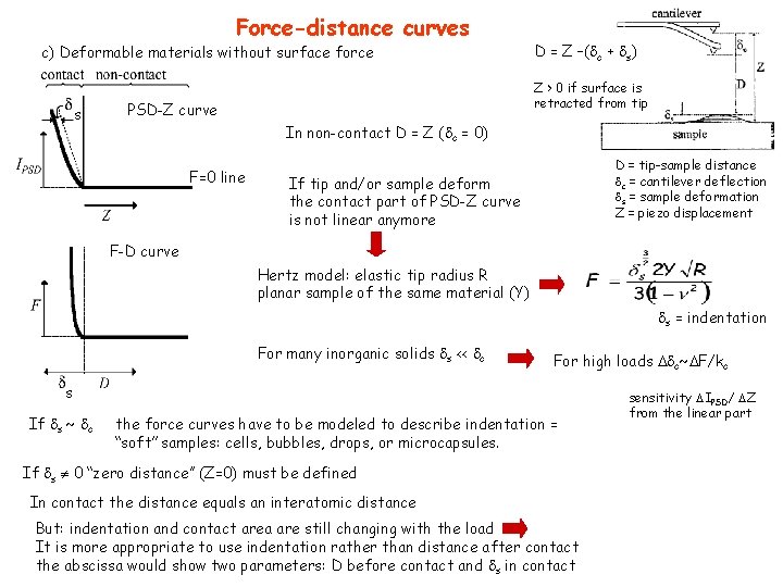
Force-distance curves c) Deformable materials without surface force s D = Z –( c + s) Z > 0 if surface is retracted from tip PSD-Z curve In non-contact D = Z ( c = 0) F=0 line D = tip-sample distance c = cantilever deflection s = sample deformation Z = piezo displacement If tip and/or sample deform the contact part of PSD-Z curve is not linear anymore F-D curve Hertz model: elastic tip radius R planar sample of the same material (Y) s = indentation For many inorganic solids s << c For high loads c~ F/kc s If s ~ c the force curves have to be modeled to describe indentation = ‘‘soft’’ samples: cells, bubbles, drops, or microcapsules. If s 0 ‘‘zero distance’’ (Z=0) must be defined In contact the distance equals an interatomic distance But: indentation and contact area are still changing with the load It is more appropriate to use indentation rather than distance after contact the abscissa would show two parameters: D before contact and s in contact sensitivity IPSD/ Z from the linear part

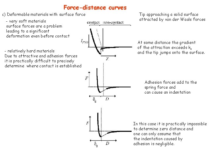
Force-distance curves c) Deformable materials with surface force Tip approaching a solid surface attracted by van der Waals forces - very soft materials surface forces are a problem leading to a significant deformation even before contact At some distance the gradient of the attraction exceeds kc and the tip jumps onto the surface. - relatively hard materials Due to attractive and adhesion forces it is practically difficult to precisely determine where contact is established Adhesion forces add to the spring force and can cause an indentation s s In this case it is practically impossible to determine zero distance and one can only assume that the indentation caused by adhesion is negligible.

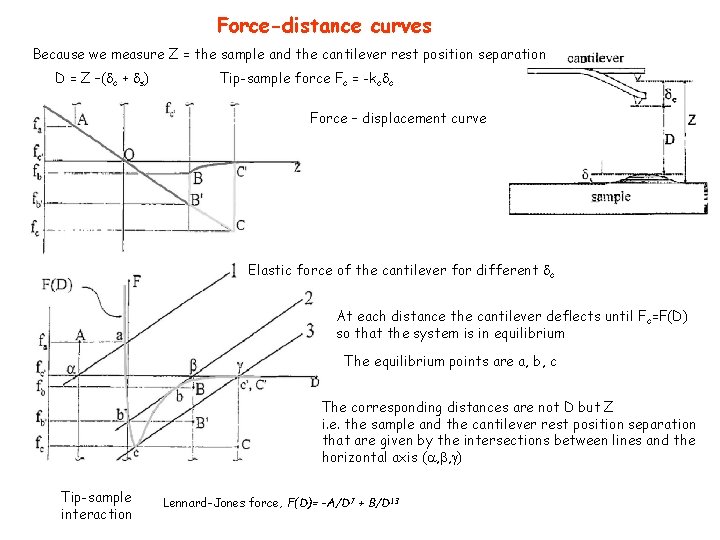
Force-distance curves Because we measure Z = the sample and the cantilever rest position separation D = Z –( c + s) Tip-sample force Fc = -kc c Force – displacement curve Elastic force of the cantilever for different c At each distance the cantilever deflects until Fc=F(D) so that the system is in equilibrium The equilibrium points are a, b, c The corresponding distances are not D but Z i. e. the sample and the cantilever rest position separation that are given by the intersections between lines and the horizontal axis ( , , ) Tip-sample interaction Lennard-Jones force, F(D)= -A/D 7 + B/D 13

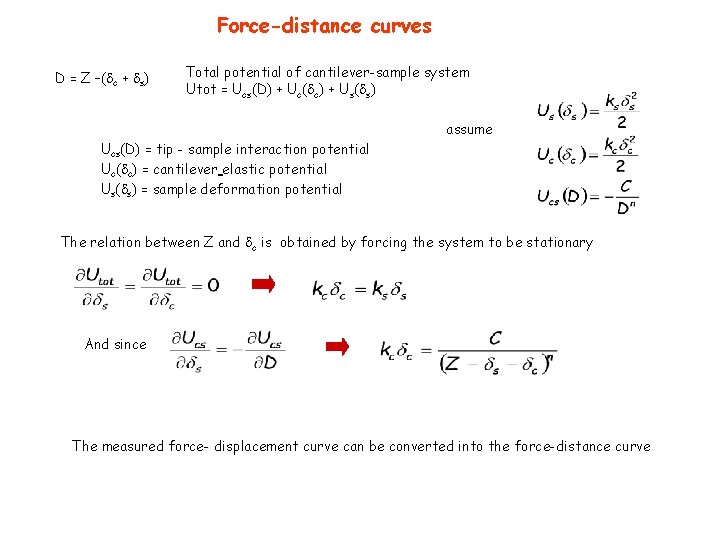
Force-distance curves D = Z –( c + s) Total potential of cantilever-sample system Utot = Ucs(D) + Uc( c) + Us( s) assume Ucs(D) = tip - sample interaction potential Uc( c) = cantilever elastic potential Us( s) = sample deformation potential The relation between Z and c is obtained by forcing the system to be stationary And since The measured force- displacement curve can be converted into the force-distance curve

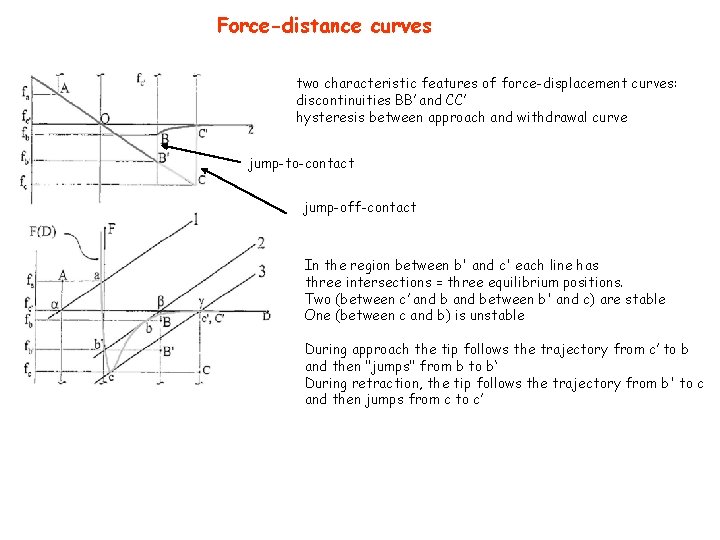
Force-distance curves two characteristic features of force-displacement curves: discontinuities BB’ and CC’ hysteresis between approach and withdrawal curve jump-to-contact jump-off-contact In the region between b' and c' each line has three intersections = three equilibrium positions. Two (between c’ and between b' and c) are stable One (between c and b) is unstable During approach the tip follows the trajectory from c’ to b and then "jumps" from b to b‘ During retraction, the tip follows the trajectory from b' to c and then jumps from c to c’

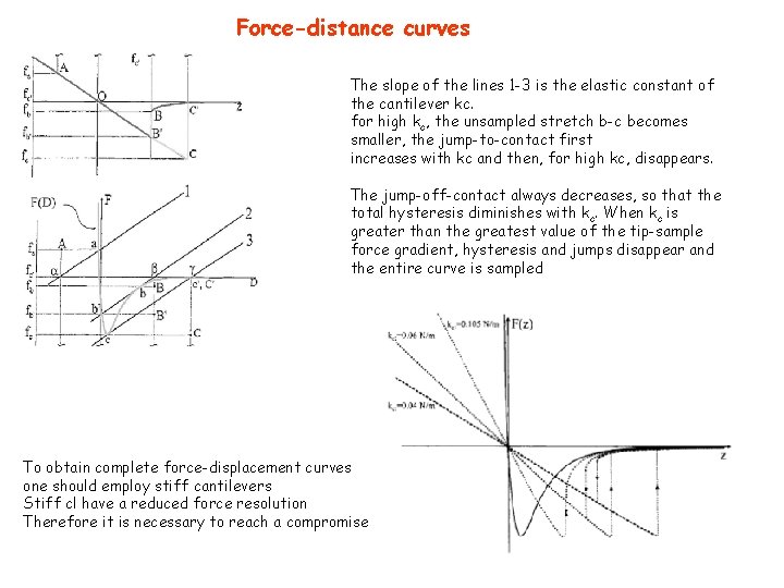
Force-distance curves The slope of the lines 1 -3 is the elastic constant of the cantilever kc. for high kc, the unsampled stretch b-c becomes smaller, the jump-to-contact first increases with kc and then, for high kc, disappears. The jump-off-contact always decreases, so that the total hysteresis diminishes with kc. When kc is greater than the greatest value of the tip-sample force gradient, hysteresis and jumps disappear and the entire curve is sampled To obtain complete force-displacement curves one should employ stiff cantilevers Stiff cl have a reduced force resolution Therefore it is necessary to reach a compromise

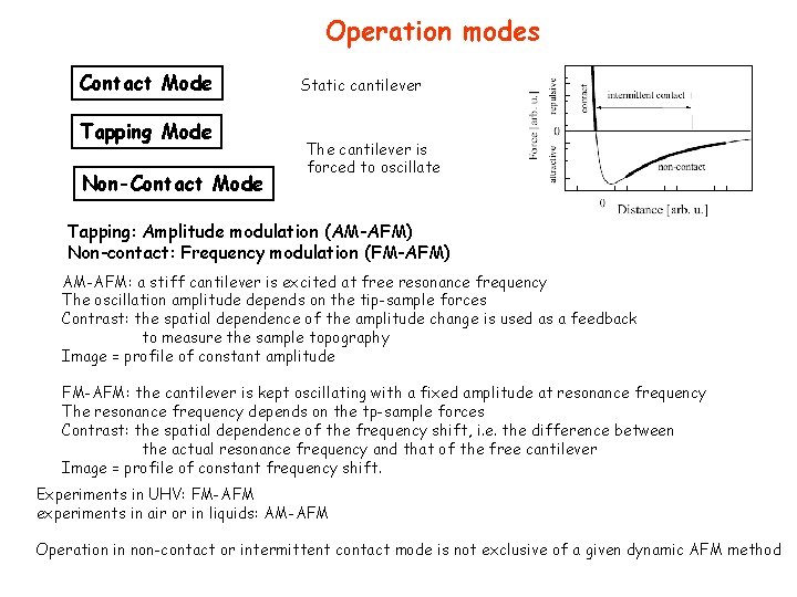
Operation modes Contact Mode Tapping Mode Non-Contact Mode Static cantilever The cantilever is forced to oscillate Tapping: Amplitude modulation (AM-AFM) Non-contact: Frequency modulation (FM-AFM) AM-AFM: a stiff cantilever is excited at free resonance frequency The oscillation amplitude depends on the tip-sample forces Contrast: the spatial dependence of the amplitude change is used as a feedback to measure the sample topography Image = profile of constant amplitude FM-AFM: the cantilever is kept oscillating with a fixed amplitude at resonance frequency The resonance frequency depends on the tp-sample forces Contrast: the spatial dependence of the frequency shift, i. e. the difference between the actual resonance frequency and that of the free cantilever Image = profile of constant frequency shift. Experiments in UHV: FM-AFM experiments in air or in liquids: AM-AFM Operation in non-contact or intermittent contact mode is not exclusive of a given dynamic AFM method

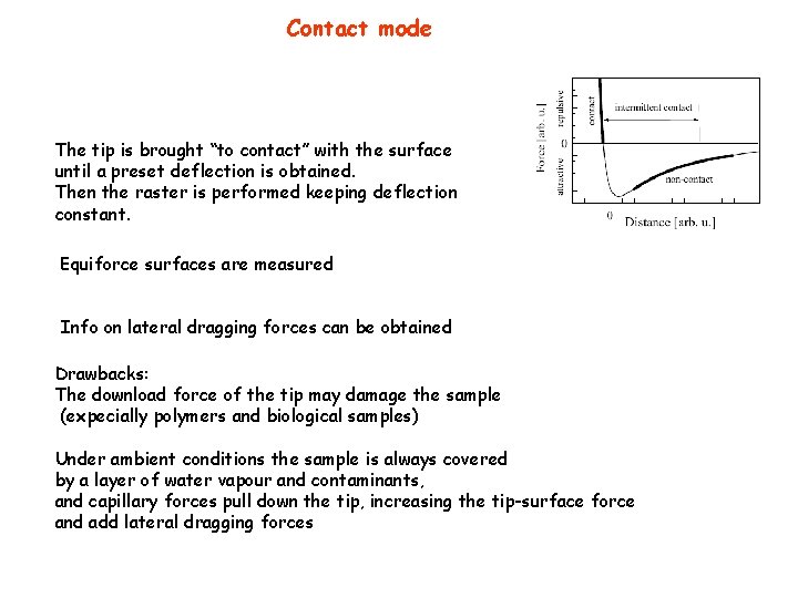
Contact mode The tip is brought “to contact” with the surface until a preset deflection is obtained. Then the raster is performed keeping deflection constant. Equiforce surfaces are measured Info on lateral dragging forces can be obtained Drawbacks: The download force of the tip may damage the sample (expecially polymers and biological samples) Under ambient conditions the sample is always covered by a layer of water vapour and contaminants, and capillary forces pull down the tip, increasing the tip-surface force and add lateral dragging forces

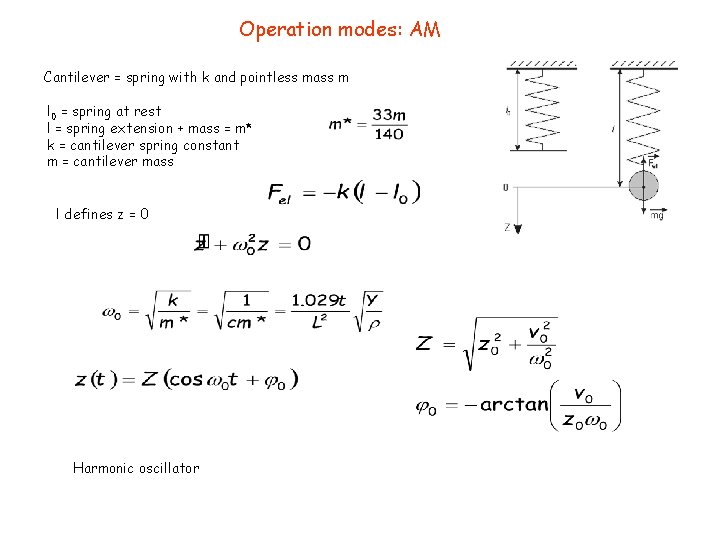
Operation modes: AM Cantilever = spring with k and pointless mass m l 0 = spring at rest l = spring extension + mass = m* k = cantilever spring constant m = cantilever mass l defines z = 0 Harmonic oscillator

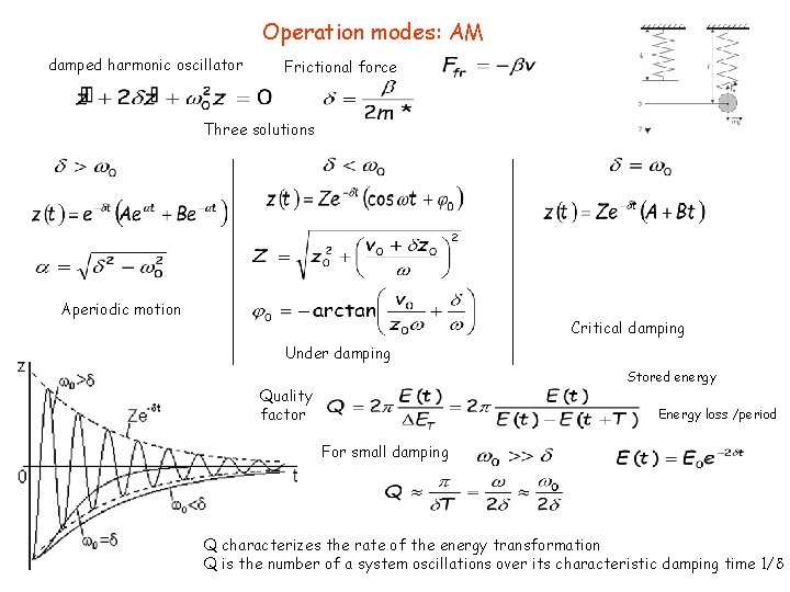
Operation modes: AM damped harmonic oscillator Frictional force Three solutions Aperiodic motion Critical damping Under damping Stored energy Quality factor Energy loss /period For small damping Q characterizes the rate of the energy transformation Q is the number of a system oscillations over its characteristic damping time 1/

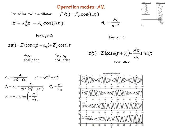
Operation modes: AM Forced harmonic oscillator For 0 free oscillation For 0 = Driving oscillation resonance

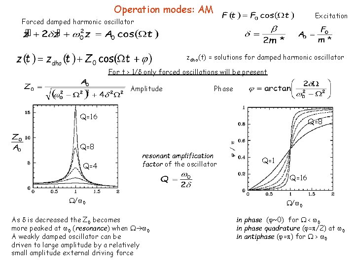
Operation modes: AM Excitation Forced damped harmonic oscillator zdho(t) = solutions for damped harmonic oscillator For t > 1/ only forced oscillations will be present Amplitude Phase Q=16 Q=8 Q=4 Q=8 resonant amplification factor of the oscillator Q=16 / 0 As is decreased the Z 0 becomes more peaked at 0 (resonance) when 0 A weakly damped oscillator can be driven to large amplitude by a relatively small amplitude external driving force / 0 in phase ( ~0) for < 0 in phase quadrature ( = /2) at 0 in antiphase ( = ) for > 0

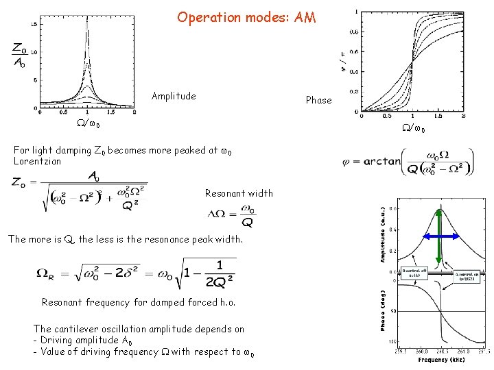
Operation modes: AM Amplitude Phase / 0 For light damping Z 0 becomes more peaked at 0 Lorentzian Resonant width The more is Q, the less is the resonance peak width. Resonant frequency for damped forced h. o. The cantilever oscillation amplitude depends on - Driving amplitude A 0 - Value of driving frequency with respect to 0

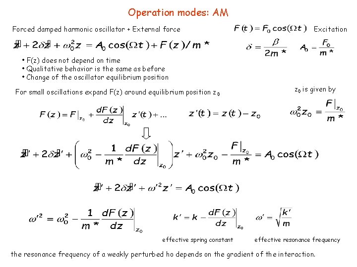
Operation modes: AM Forced damped harmonic oscillator + External force Excitation • F(z) does not depend on time • Qualitative behavior is the same as before • Change of the oscillator equilibrium position For small oscillations expand F(z) around equilibrium position z 0 effective spring constant z 0 is given by effective resonance frequency the resonance frequency of a weakly perturbed ho depends on the gradient of the interaction.

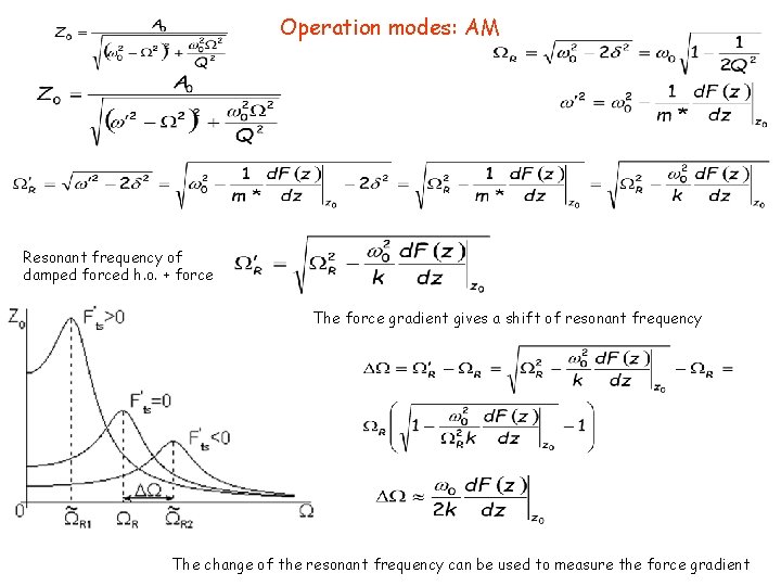
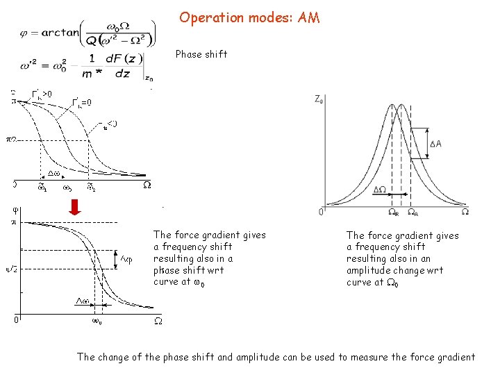
Operation modes: AM Resonant frequency of damped forced h. o. + force The force gradient gives a shift of resonant frequency The change of the resonant frequency can be used to measure the force gradient

Operation modes: AM Phase shift The force gradient gives a frequency shift resulting also in a phase shift wrt curve at 0 The force gradient gives a frequency shift resulting also in an amplitude change wrt curve at 0 The change of the phase shift and amplitude can be used to measure the force gradient

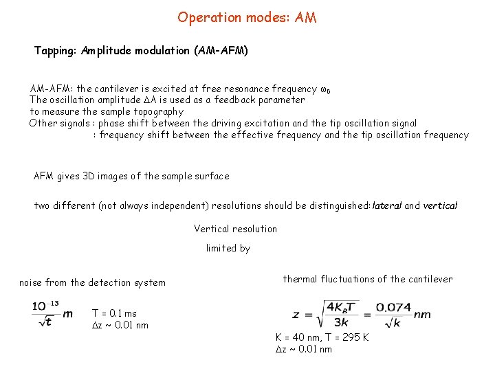
Operation modes: AM Tapping: Amplitude modulation (AM-AFM) AM-AFM: the cantilever is excited at free resonance frequency 0 The oscillation amplitude A is used as a feedback parameter to measure the sample topography Other signals : phase shift between the driving excitation and the tip oscillation signal : frequency shift between the effective frequency and the tip oscillation frequency AFM gives 3 D images of the sample surface two different (not always independent) resolutions should be distinguished: lateral and vertical Vertical resolution limited by noise from the detection system T = 0. 1 ms z ~ 0. 01 nm thermal fluctuations of the cantilever K = 40 nm, T = 295 K z ~ 0. 01 nm

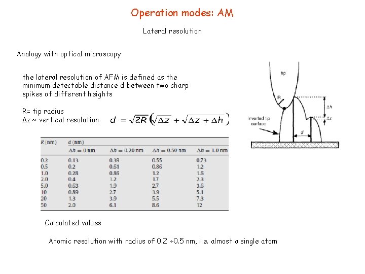
Operation modes: AM Lateral resolution Analogy with optical microscopy the lateral resolution of AFM is defined as the minimum detectable distance d between two sharp spikes of different heights R= tip radius z ~ vertical resolution Calculated values Atomic resolution with radius of 0. 2 0. 5 nm, i. e. almost a single atom

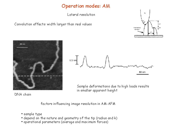
Operation modes: AM Lateral resolution Convolution effects: width larger than real values DNA chain Sample deformations due to high loads results in smaller apparent height factors influencing image resolution in AM-AFM • sample type • depend on the nature and geometry of the tip (radius and k) • operational parameters (average and maximum forces)

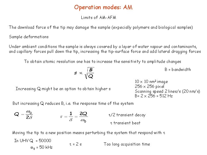
Operation modes: AM Limits of AM-AFM The download force of the tip may damage the sample (expecially polymers and biological samples) Sample deformations Under ambient conditions the sample is always covered by a layer of water vapour and contaminants, and capillary forces pull down the tip, increasing the tip-surface force and add lateral dragging forces To obtain atomic resolution one has to increase the sensitivity to amplitude changes B = bandwidth Increasing Q might be an option to obtain higher s 10 x 10 nm 2 image 256 x 256 pixel Scanning speed 2 lines/s (20 nm/s) B= 2 x 256 = 512 Hz But increasing Q reduces B, i. e. the response time of the system /2 transient decay transient beat Moving the tip to a new position means perturbing the system that respond with In UHV Q = 50000 0 = 50 k. Hz =2 s Too long acquisition time

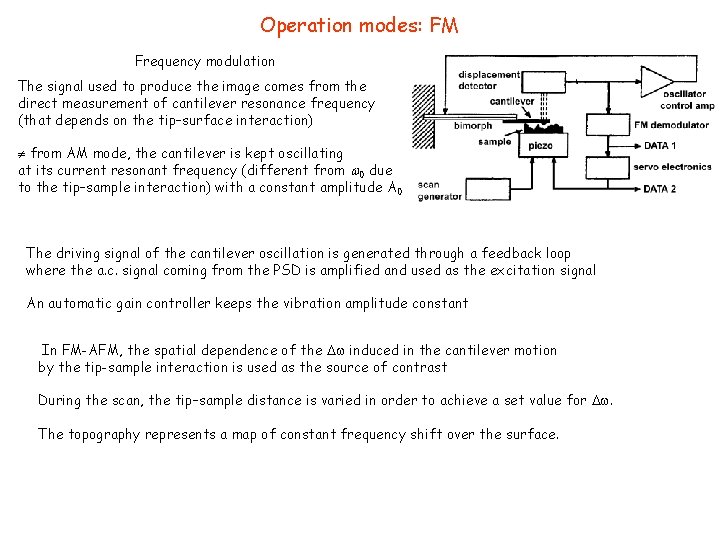
Operation modes: FM Frequency modulation The signal used to produce the image comes from the direct measurement of cantilever resonance frequency (that depends on the tip–surface interaction) from AM mode, the cantilever is kept oscillating at its current resonant frequency (different from 0 due to the tip–sample interaction) with a constant amplitude A 0 The driving signal of the cantilever oscillation is generated through a feedback loop where the a. c. signal coming from the PSD is amplified and used as the excitation signal An automatic gain controller keeps the vibration amplitude constant In FM-AFM, the spatial dependence of the induced in the cantilever motion by the tip-sample interaction is used as the source of contrast During the scan, the tip–sample distance is varied in order to achieve a set value for . The topography represents a map of constant frequency shift over the surface.

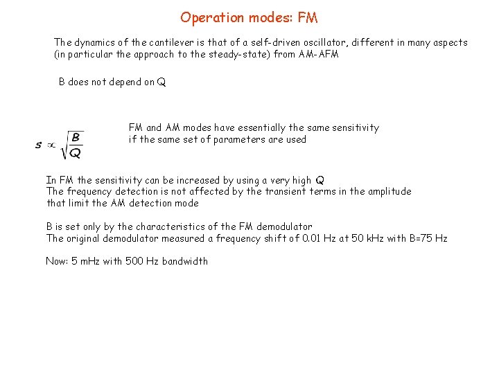
Operation modes: FM The dynamics of the cantilever is that of a self-driven oscillator, different in many aspects (in particular the approach to the steady-state) from AM-AFM B does not depend on Q FM and AM modes have essentially the same sensitivity if the same set of parameters are used In FM the sensitivity can be increased by using a very high Q The frequency detection is not affected by the transient terms in the amplitude that limit the AM detection mode B is set only by the characteristics of the FM demodulator The original demodulator measured a frequency shift of 0. 01 Hz at 50 k. Hz with B=75 Hz Now: 5 m. Hz with 500 Hz bandwidth

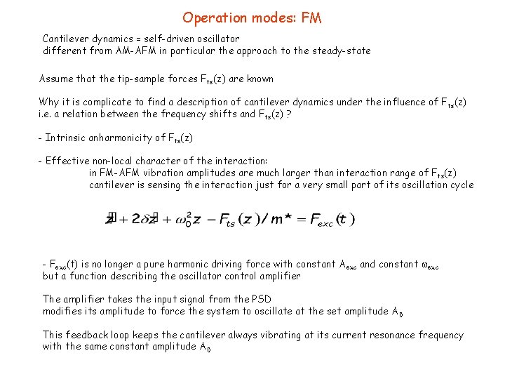
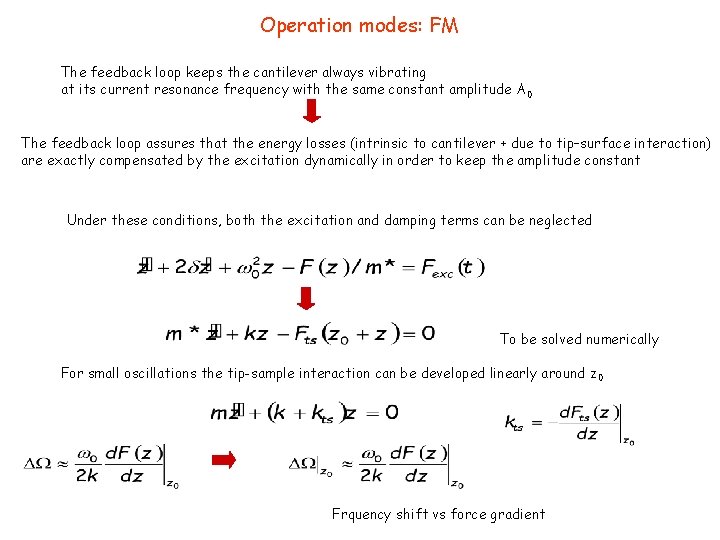
Operation modes: FM Cantilever dynamics = self-driven oscillator different from AM-AFM in particular the approach to the steady-state Assume that the tip-sample forces Fts(z) are known Why it is complicate to find a description of cantilever dynamics under the influence of F ts(z) i. e. a relation between the frequency shifts and Fts(z) ? - Intrinsic anharmonicity of Fts(z) - Effective non-local character of the interaction: in FM-AFM vibration amplitudes are much larger than interaction range of F ts(z) cantilever is sensing the interaction just for a very small part of its oscillation cycle - Fexc(t) is no longer a pure harmonic driving force with constant A exc and constant exc but a function describing the oscillator control amplifier The amplifier takes the input signal from the PSD modifies its amplitude to force the system to oscillate at the set amplitude A 0 This feedback loop keeps the cantilever always vibrating at its current resonance frequency with the same constant amplitude A 0

Operation modes: FM The feedback loop keeps the cantilever always vibrating at its current resonance frequency with the same constant amplitude A 0 The feedback loop assures that the energy losses (intrinsic to cantilever + due to tip–surface interaction) are exactly compensated by the excitation dynamically in order to keep the amplitude constant Under these conditions, both the excitation and damping terms can be neglected To be solved numerically For small oscillations the tip-sample interaction can be developed linearly around z 0 Frquency shift vs force gradient

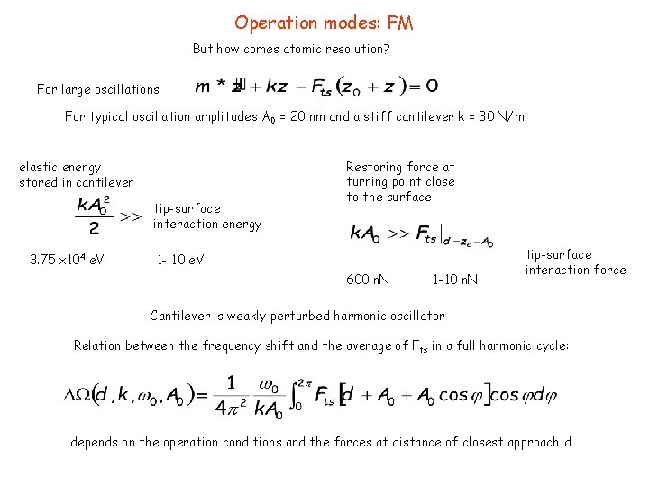
Operation modes: FM But how comes atomic resolution? For large oscillations For typical oscillation amplitudes A 0 = 20 nm and a stiff cantilever k = 30 N/m elastic energy stored in cantilever tip-surface interaction energy 3. 75 x 104 e. V Restoring force at turning point close to the surface 1 - 10 e. V 600 n. N 1 -10 n. N tip-surface interaction force Cantilever is weakly perturbed harmonic oscillator Relation between the frequency shift and the average of F ts in a full harmonic cycle: depends on the operation conditions and the forces at distance of closest approach d

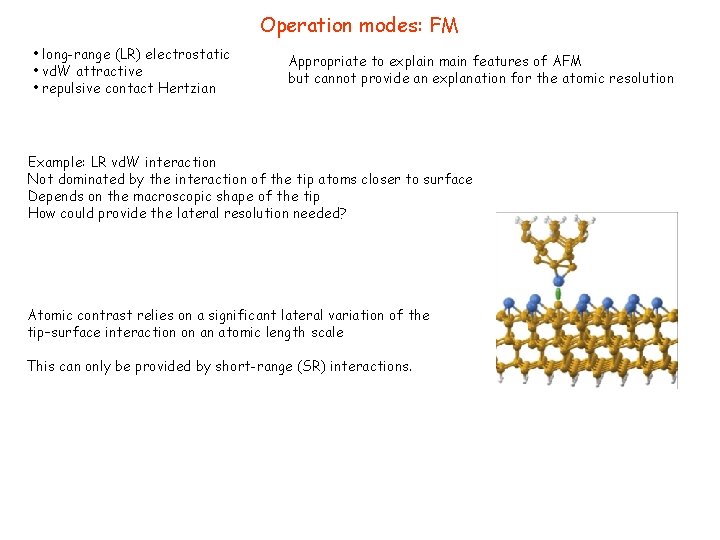
Operation modes: FM • long-range (LR) electrostatic • vd. W attractive • repulsive contact Hertzian Appropriate to explain main features of AFM but cannot provide an explanation for the atomic resolution Example: LR vd. W interaction Not dominated by the interaction of the tip atoms closer to surface Depends on the macroscopic shape of the tip How could provide the lateral resolution needed? Atomic contrast relies on a significant lateral variation of the tip–surface interaction on an atomic length scale This can only be provided by short-range (SR) interactions.

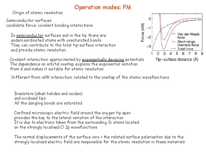
Origin of atomic resolution Operation modes: FM Semiconductor surfaces candidate force: covalent bonding interactions In semiconductor surfaces and in the tip there are undercoordinated atoms with unsaturated bonds They can contribute to the total tip–surface interaction and provide atomic resolution. Covalent interaction: approximated by exponentially decaying potentials The dependence on orbital overlap explains the exponential variation from d and makes it suitable for atomic resolution Different from vd. W interaction: related to the overlap of the atomic wavefunctions Insulators (alkali halides and oxides) and oxidised tips All the dangling bonds are saturated Confined microscopic electric field around the oxygen tip apex provides the key to the lateral variation of the interaction It is due to electrons taken from the surrounding Si atoms located on the strongly localised O 2 p wavefunctions The normal displacements of the surface ions + the related surface polarisation due to the strongly localised electric field are responsible for the atomic resolution in these materials

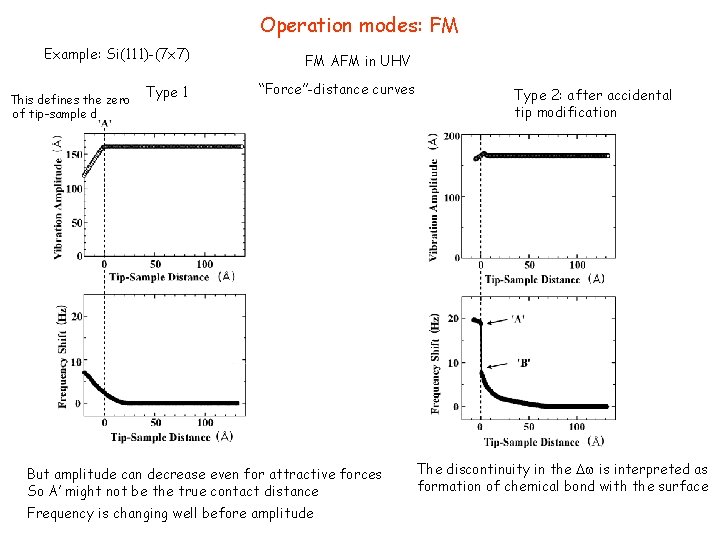
Operation modes: FM Example: Si(111)-(7 x 7) This defines the zero of tip-sample d Type 1 FM AFM in UHV “Force”-distance curves But amplitude can decrease even for attractive forces So A’ might not be the true contact distance Frequency is changing well before amplitude Type 2: after accidental tip modification The discontinuity in the is interpreted as formation of chemical bond with the surface

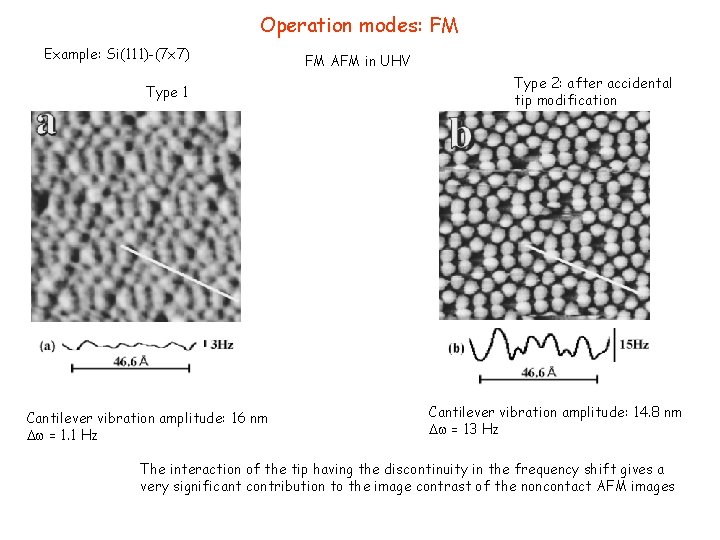
Operation modes: FM Example: Si(111)-(7 x 7) Type 1 Cantilever vibration amplitude: 16 nm = 1. 1 Hz FM AFM in UHV Type 2: after accidental tip modification Cantilever vibration amplitude: 14. 8 nm = 13 Hz The interaction of the tip having the discontinuity in the frequency shift gives a very significant contribution to the image contrast of the noncontact AFM images

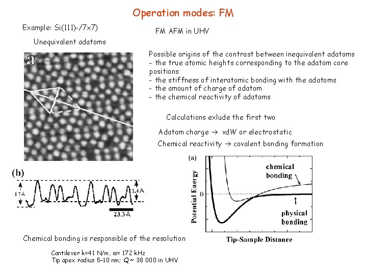
Operation modes: FM Example: Si(111)-/7 x 7) FM AFM in UHV Unequivalent adatoms Possible origins of the contrast between inequivalent adatoms - the true atomic heights corresponding to the adatom core positions - the stiffness of interatomic bonding with the adatoms - the amount of charge of adatom - the chemical reactivity of adatoms Calculations exlude the first two Adatom charge vd. W or electrostatic Chemical reactivity covalent bonding formation Chemical bonding is responsible of the resolution Cantilever k=41 N/m, = 172 k. Hz Tip apex radius 5– 10 nm; Q ~ 38 000 in UHV