Magnetic Tunnel Junction MTJ or Tunnel Magnetoresistance TMR
 or Tunnel Magnetoresistance (TMR) or Junction Magneto- Resistance (JMR) T.")

 FM II (PII) e. V Barrier")
 Double barrier junction FM")
")
 I Exchange coupling HEXB HCF HS HCP")


 - Non-volatile logic")


- Slides: 40
Magnetic Tunnel Junction (MTJ) or Tunnel Magnetoresistance (TMR) or Junction Magneto- Resistance (JMR) T. Stobiecki Katedra Elektroniki AGH 11 wykład 13. 12. 2004
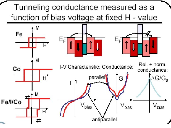
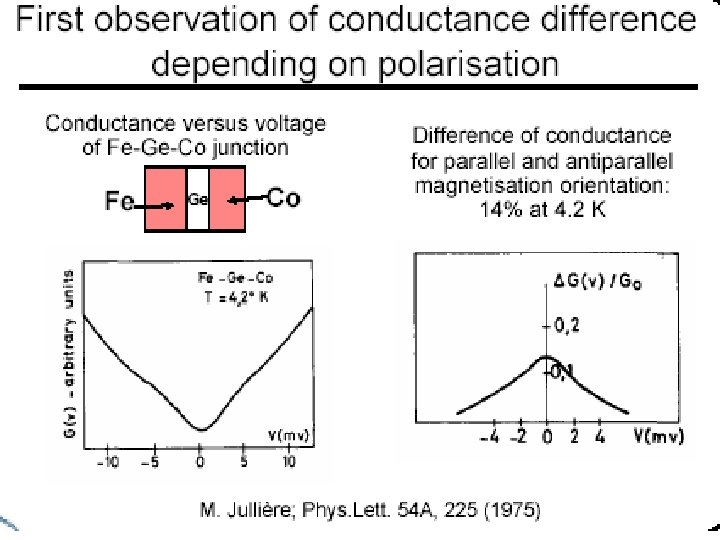
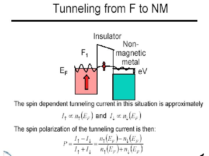
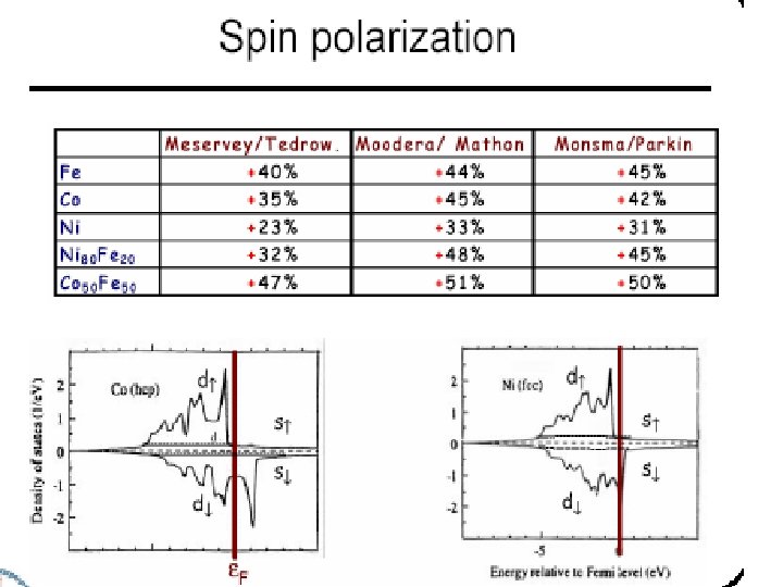
Spin Polarization, Density of States Spin Polarization Density of states 3 d Ferromagnetic metal (Fe) Material Polarizations Ni 33 % Co 42 % Fe 45 % Ni 80 Fe 20 48 % Co 84 Fe 16 55 % Co. Fe. B 60% Normal metal (Cu)
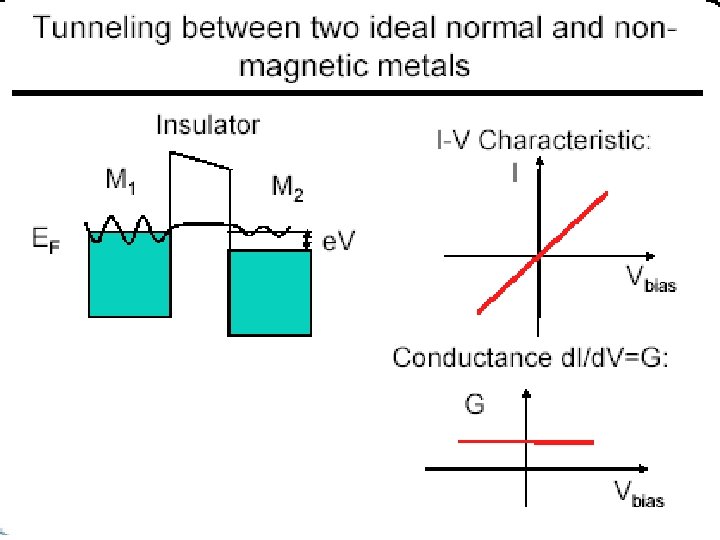
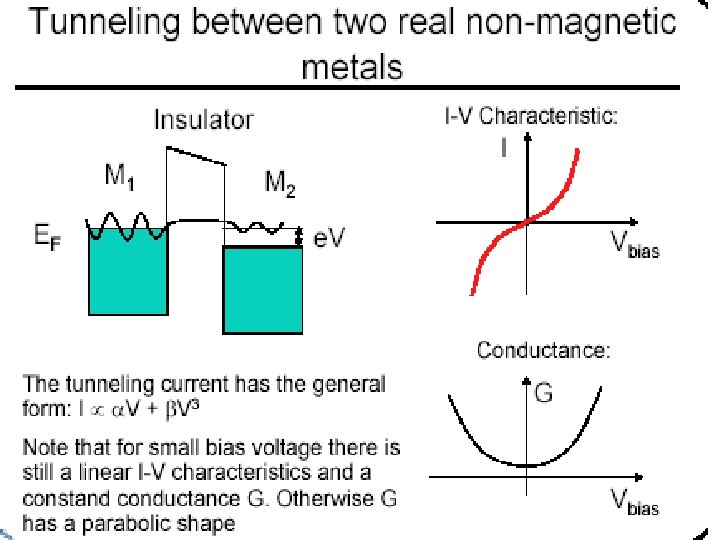
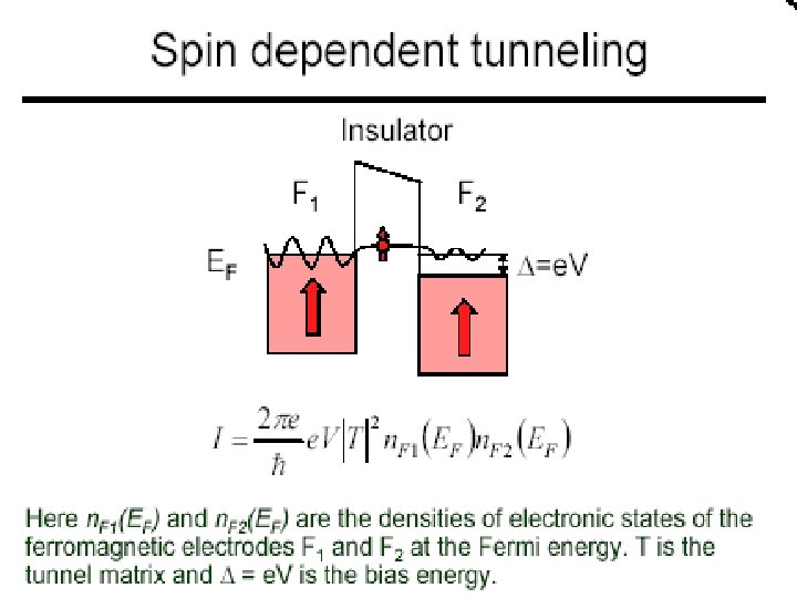
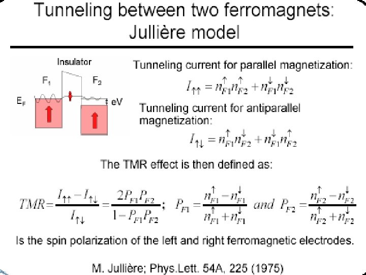
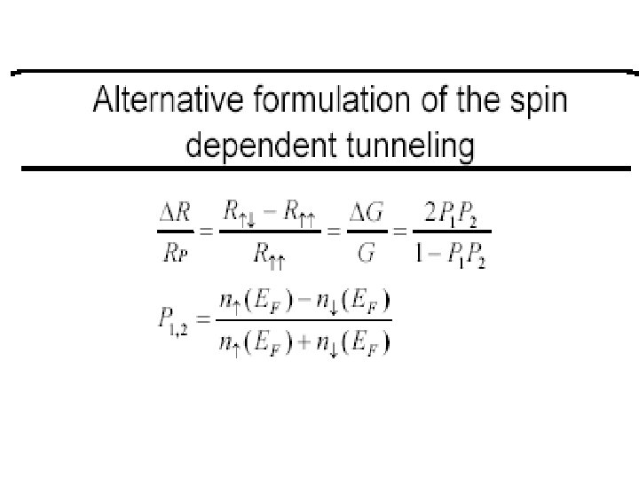
Tunneling in FM/I/FM junction FM I (PI) FM II (PII) e. V Barrier
Type of MTJs Standard junction Spin valve junction (SV- MTJ) Double barrier junction FM FM FM I I I FM FM AF I B FM
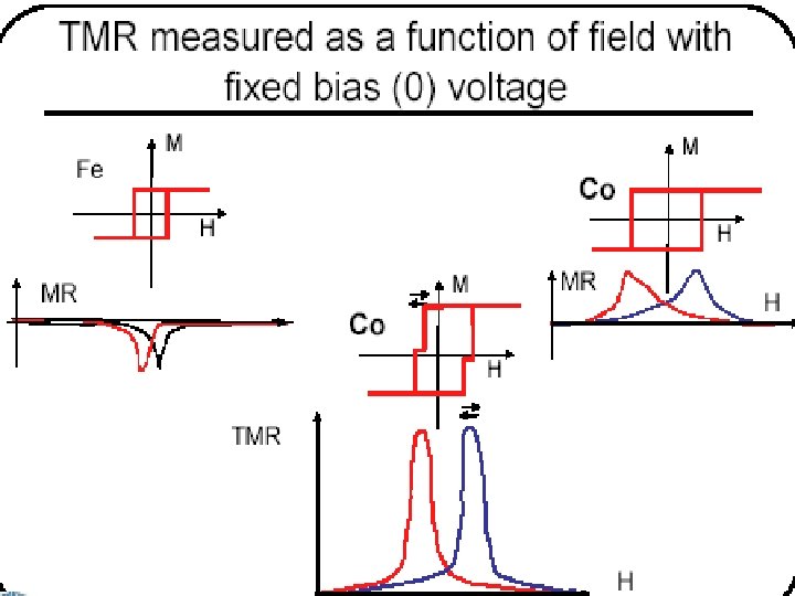
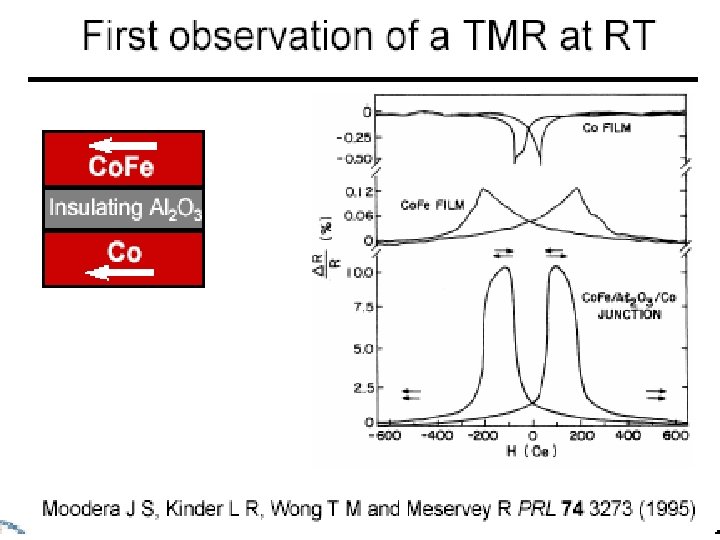
Application-Oriented Properties of S-V MTJ Materials SV-MTJ • I (Al-O, Mg. O. . ) Treatment • FM (Co, Co. Fe, Ni. Fe) Preparation • Annealing • AF (Mn. Ir, Pt. Mn, Ni. O) • Sputtering deposition • Field cooling • Buffer (Ta, Cu, Ni. Fe) • Oxidation Electric • Tunnel Magnetoresistance -TMR • Resistance area product -Rx. A Magnetic • Interlayer coupling field HS • Exchange bias field HEXB • Coercive field pinned HCP and free HCF layer • Switching field HSF
Magnetic and Electric Parameters FM I (Free) I Exchange coupling HEXB HCF HS HCP HEXB HSF switching fields FM II (Pinned) AF B Interlayer coupling HS
Applications of SV-MTJ SENSORS M-RAM SV-MTJ SPIN-LOGIC READ HEADS
SV-MTJ Based MRAM Writing - rotation of the free layer Reading - detection of a resistance of a junction Critical switching fields Hx , Hy (S-W) asteroid 1 Hy/H(0) SV- MTJ as MRAM component must fulfill requirements - Thermal stability - Magnetic stability - Single domain like switching behaviour - Reproducibility of Rx. A, TMR and Asteroids 0 Motorola: S. Tehrani et al. PROCEEDINGS OF THE IEEE, VOL. 91, NO. 5, MAY 2003 -1 -1 0 1
- Non-volatility of FLASH with fast programming, no program endurance limitation - Density competitive with DRAM, with no refresh - Speed competitive with SRAM - Nondestructive read - Resistance to ionization radiation - Low power consumption (current pulses) Features of M-RAM • Single 3. 3 V power supply • Commercial temperature range (0°C to 70°C) • Symmetrical high-speed read and write with fast access time (15, 20 or 25 ns) • Flexible data bus control — 8 bit or 16 bit access • Equal address and chip-enable access times • All inputs and outputs are transistor-transistor logic (TTL) compatible • Full nonvolatile operation with 10 years minimum data retention Motorola: S. Tehrani et al. PROCEEDINGS OF THE IEEE, VOL. 91, NO. 5, MAY 2003
SV-MTJ Based Spin Logic Gates VOUT= IS(RMTJ 3 + RMTJ 3 – RMTJ 1 – RMTJ 2) SV- MTJ as spin logic gates must fulfill requirements - Thermal stability - Magnetic stability - Centered minor loop - Single domain like switching behaviour - Reproducibility of R, TMR Siemens & Univ. Bielefeld: R. Richter et al. J. Magn. Mat. 240 (2002) 127– 129
Features of Spin Logic Gates - Programmable logic functions (reconfigurable computing) - Non-volatile logic inputs and outputs - Fast operation (up to 5 GHz) - Low power consumption - Compatibility to M-RAM
SV-MTJ Based Read Heads SV-MTJ as a read sensor for high density (> 100 Gb/in 2) must fulfill requirements - Resistance area product (Rx. A) < 6 - m 2 - High TMR at low Rx. A
A MTJs. Experiments on SV -MTJs B MTJs Ta 5 nm Au 25 nm Ni. Fe x nm Ta 3 nm Junction Cu 30 nm Co. Fe 2. 5 nm 0 10 30 60 100 Al 2 O 3 1. 4 nm Junctions size (180 180) m 2 Co. Fe 2. 5 nm Ta 5 nm Mn. Ir 10 nm Ni. Fe 3 nm Cu 5 nm Junction Al 2 O 3 1. 4 nm Co. Fe t nm Mn. Ir 12 nm 3 6 10 30 50 Ni. Fe 2 nm Ta 5 nm Cu 10 nm Cu 25 nm Ta 5 nm Substrate Si (100) Si. O 2 Substrate Si (100) A structure prof. G. Reiss laboratory University Bielefeld B structure prof. T. Takahasi laboratory, Tohoku University 10 mm
Effect of Annealing on TMR As deposited H=80 k. A/m 10 mm annealing 1 hour in vacuum 10 -6 h. Pa Annealed
Interlayer and Exchange Coupling Fields Exchange coupling fields A MTJs Interlayer coupling fields B MTJs
Interlayer and Exchange Coupling Fields
Temperature Dependence of TMR P. Wiśniowski, M. Rams, . . . Temperature dependence of tunnel magnetoresistance of Ir. Mn based MTJ, phys. stat. sol (2004)
Total Conductance Varies slightly with T Negligible Varies with T as magnetization does Bloch law Dominant
Polarization, Bloch Law 1. Set H= – 2000 Oe 2. Cooling H= 500 Oe 1. Set H= – 2000 Oe 3. Measured M (T) 2. Cooling H= – 500 Oe 3. Measured M (T) P 100 nm AP
Spin Independent Conductance Hopping conductance, high level of defects Hopping conductance, low level of defects
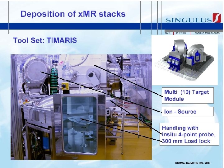
TIMARIS: Tool status Tool #1 – process optimization on 200 mm wafers since mid of March 03 Tool #2 – The Worlds 1 st 300 mm MRAM System is Ready for Process in August 03 Clean room Multi (10) Target Module Oxidation / Pre-clean Module Transport Module
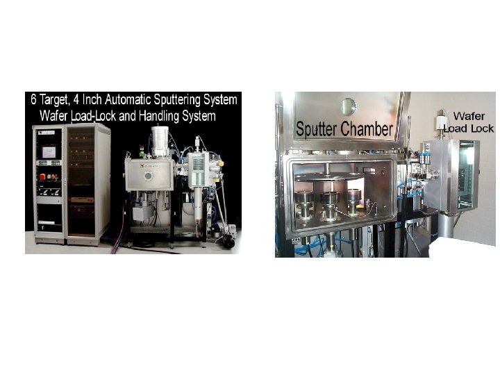
Sputtering System LL1: wafer-in Plasma Oxidation LL2: Bridge Metal depo. Reactive sputter : surface smooth
MOKE Measurements R-VSM
MOKE with Orthogonal Coils