REFERENCE CIRCUITS A reference circuit is an independent




- Slides: 38

REFERENCE CIRCUITS A reference circuit is an independent voltage or current source which has a high degree of precision and stability. • Output voltage/current should be independent of power supply. • Output voltage/current should be independent of temperature. • Output voltage/current should be independent of processing variations.

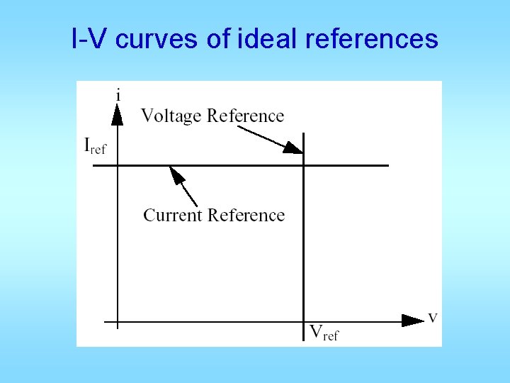
I-V curves of ideal references

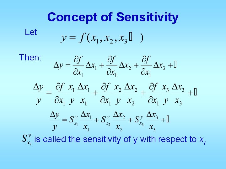
Concept of Sensitivity Let Then: is called the sensitivity of y with respect to xi

Total percentage change in y = Sensitivity w. r. t. x 1 * percentage change in x 1 + Sensitivity w. r. t. x 2 * percentage change in x 2 + …… Goal: Design reference circuits so that the reference’s sensitivities w. r. t. various variations are minimized.

Types of commonly used references • • Voltage dividers - passive and active. MOS diode reference. PN junction diode reference. Gate-source threshold reference circuit. Base-emitter reference circuit. Thermo voltage reference circuit Bandgap reference circuit

Typical variations affecting the references • Power supply variation (main concern here) • Load variation (want ro=∞ for I-ref, ro=0 for V-ref) • Temperature variation (main concern also) • Processes variation (use good process and layout) • Interferences and noise (not considered here)

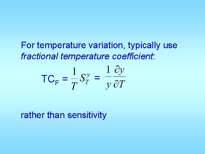
For temperature variation, typically use fractional temperature coefficient: TCF = = rather than sensitivity

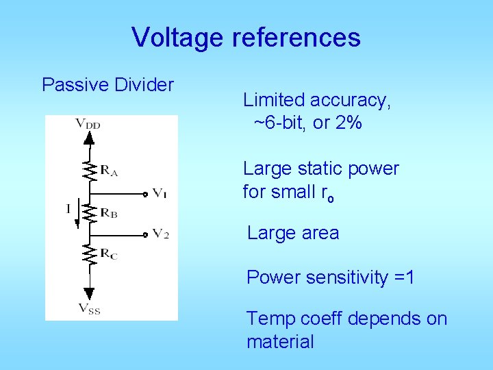
Voltage references Passive Divider Limited accuracy, ~6 -bit, or 2% Large static power for small ro Large area Power sensitivity =1 Temp coeff depends on material

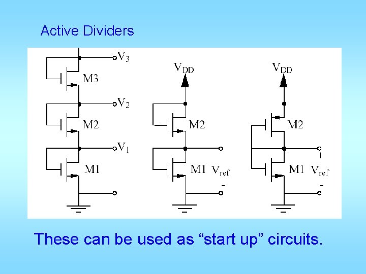
Active Dividers These can be used as “start up” circuits.

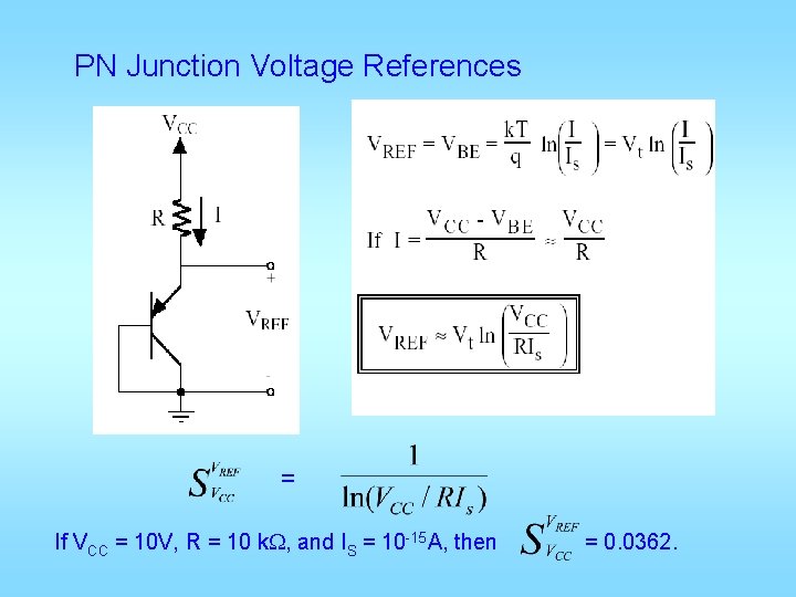
PN Junction Voltage References = If VCC = 10 V, R = 10 k. W, and IS = 10 -15 A, then = 0. 0362.

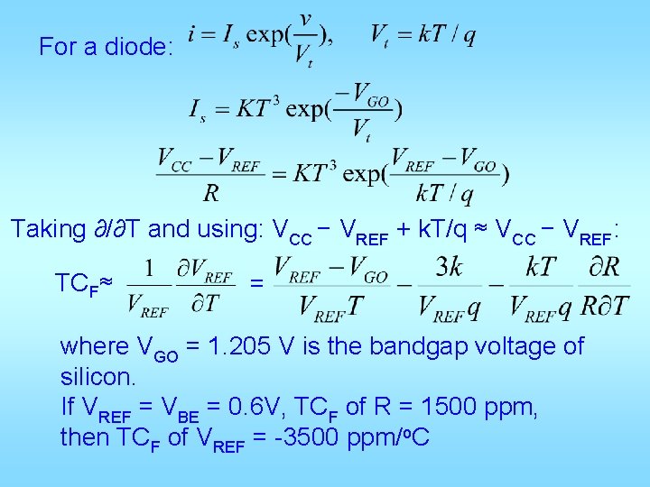
For a diode: Taking ∂/∂T and using: VCC − VREF + k. T/q ≈ VCC − VREF: TCF≈ = where VGO = 1. 205 V is the bandgap voltage of silicon. If VREF = VBE = 0. 6 V, TCF of R = 1500 ppm, then TCF of VREF = -3500 ppm/o. C

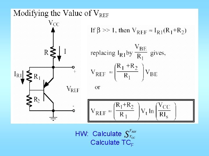
HW: Calculate TCF

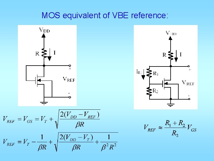
MOS equivalent of VBE reference:


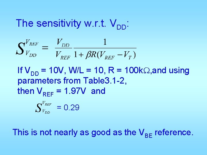
The sensitivity w. r. t. VDD: If VDD = 10 V, W/L = 10, R = 100 k. W, and using parameters from Table 3. 1 -2, then VREF = 1. 97 V and = 0. 29 This is not nearly as good as the VBE reference.

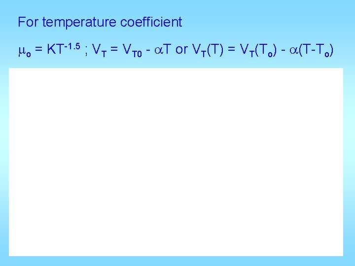
For temperature coefficient mo = KT-1. 5 ; VT = VT 0 - a. T or VT(T) = VT(To) - a(T-To)

Solving for ∂VREF/∂T and computer TC: The book has one example of using this.

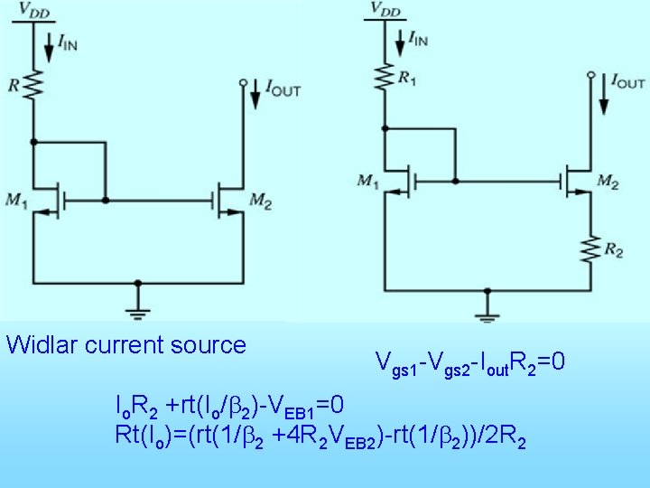
Widlar current source Vgs 1 -Vgs 2 -Iout. R 2=0 Io. R 2 +rt(Io/b 2)-VEB 1=0 Rt(Io)=(rt(1/b 2 +4 R 2 VEB 2)-rt(1/b 2))/2 R 2

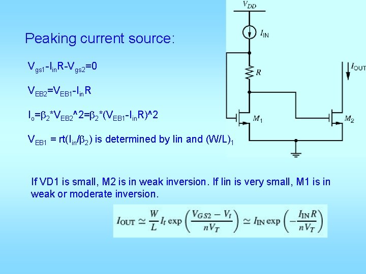
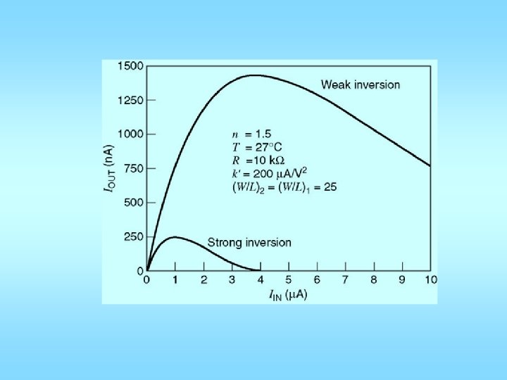
Peaking current source: Vgs 1 -Iin. R-Vgs 2=0 VEB 2=VEB 1 -Iin. R Io=b 2*VEB 2^2=b 2*(VEB 1 -Iin. R)^2 VEB 1 = rt(Iin/b 2) is determined by Iin and (W/L)1 If VD 1 is small, M 2 is in weak inversion. If Iin is very small, M 1 is in weak or moderate inversion.


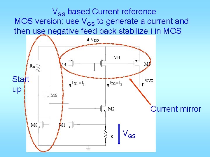
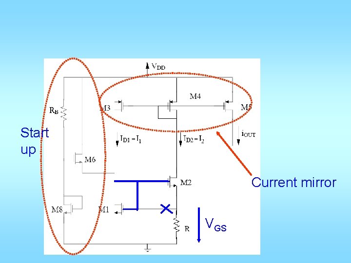
VGS based Current reference MOS version: use VGS to generate a current and then use negative feed back stabilize i in MOS Start up Current mirror VGS

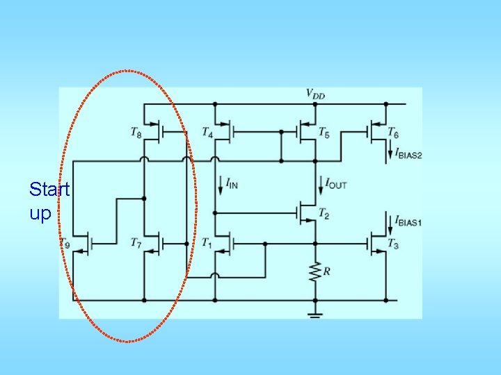
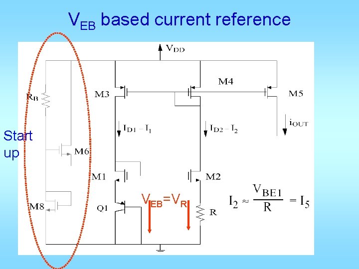
Why the start up circuit? There are two possible operating points: The desired one and The one that gives I 1 = I 2 = 0. At power up, I 1 = I 2 = 0 without the start up. RB bias M 6 to be on, which turns M 2 and M 1 on.

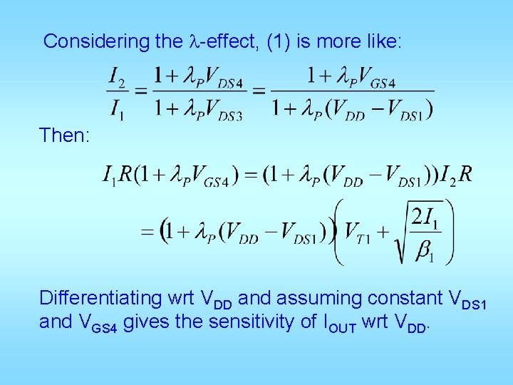
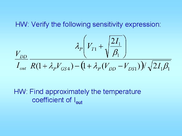
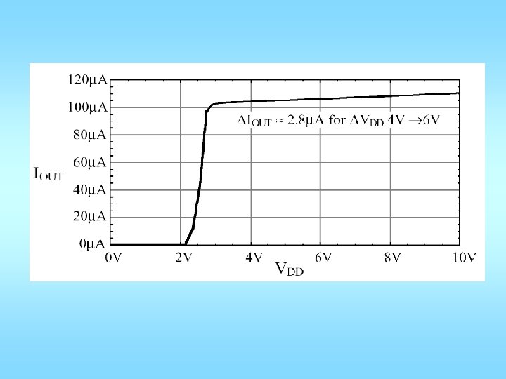
Considering the l-effect, (1) is more like: Then: Differentiating wrt VDD and assuming constant VDS 1 and VGS 4 gives the sensitivity of IOUT wrt VDD.

HW: Verify the following sensitivity expression: HW: Find approximately the temperature coefficient of Iout


Start up

Start up Current mirror VGS

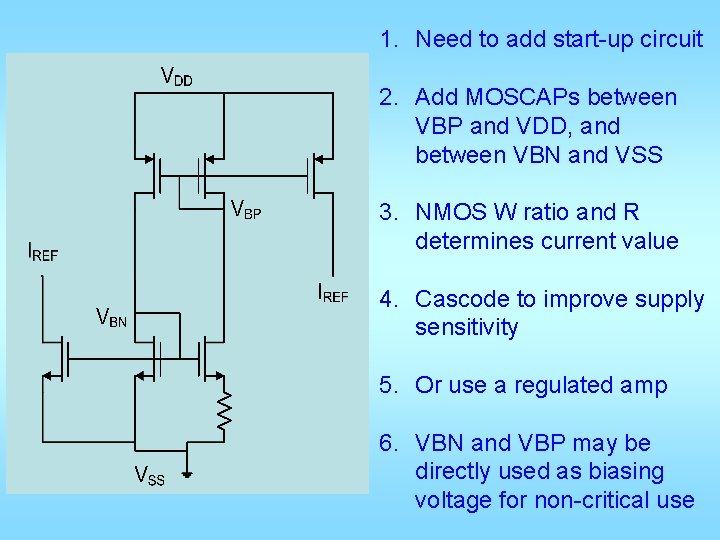
1. Need to add start-up circuit 2. Add MOSCAPs between VBP and VDD, and between VBN and VSS 3. NMOS W ratio and R determines current value 4. Cascode to improve supply sensitivity 5. Or use a regulated amp 6. VBN and VBP may be directly used as biasing voltage for non-critical use

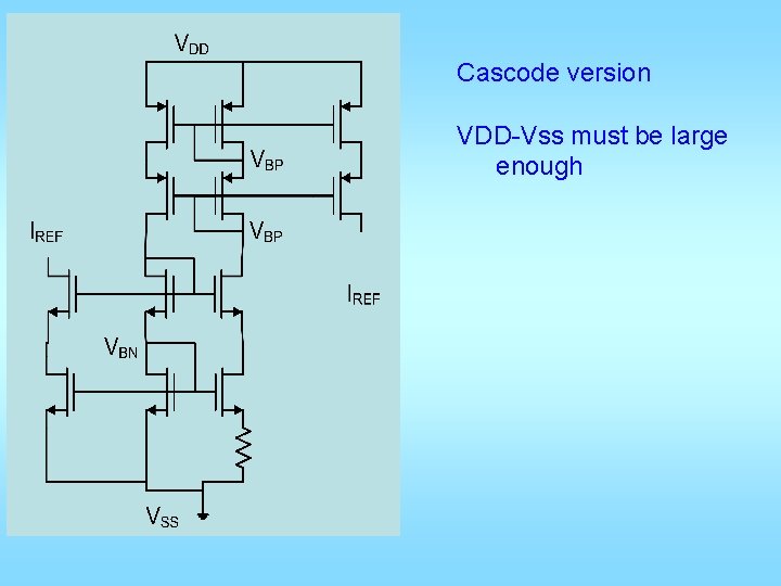
Cascode version VDD-Vss must be large enough

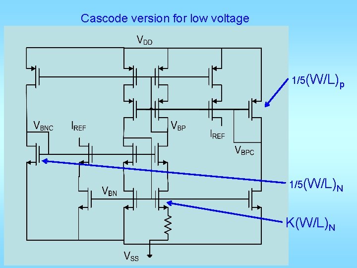
Cascode version for low voltage 1/5(W/L)p 1/5(W/L)N K(W/L)N

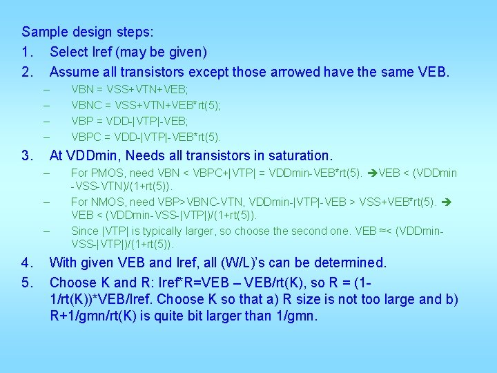
Sample design steps: 1. Select Iref (may be given) 2. Assume all transistors except those arrowed have the same VEB. – – 3. At VDDmin, Needs all transistors in saturation. – – – 4. 5. VBN = VSS+VTN+VEB; VBNC = VSS+VTN+VEB*rt(5); VBP = VDD-|VTP|-VEB; VBPC = VDD-|VTP|-VEB*rt(5). For PMOS, need VBN < VBPC+|VTP| = VDDmin-VEB*rt(5). VEB < (VDDmin -VSS-VTN)/(1+rt(5)). For NMOS, need VBP>VBNC-VTN, VDDmin-|VTP|-VEB > VSS+VEB*rt(5). VEB < (VDDmin-VSS-|VTP|)/(1+rt(5)). Since |VTP| is typically larger, so choose the second one. VEB ≈< (VDDmin. VSS-|VTP|)/(1+rt(5)). With given VEB and Iref, all (W/L)’s can be determined. Choose K and R: Iref*R=VEB – VEB/rt(K), so R = (11/rt(K))*VEB/Iref. Choose K so that a) R size is not too large and b) R+1/gmn/rt(K) is quite bit larger than 1/gmn.

VEB based current reference Start up VEB=VR

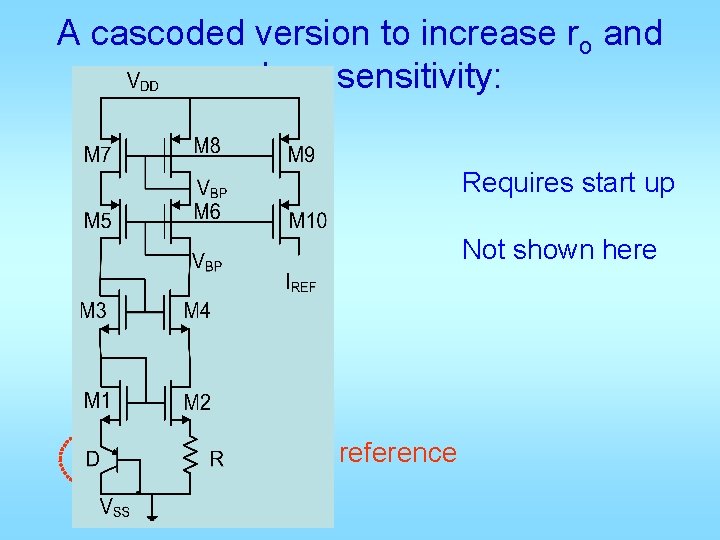
A cascoded version to increase ro and reduce sensitivity: Requires start up Not shown here VEB reference

HW: Analyze the sensitivity of the output I with respect to VDD and temperature. Come up with a start up circuit for the circuit on the previous slide, using only active resisters without RB. Note that you need to make sure that at the desired operating point, the connection from the start up circuit should be turned off.

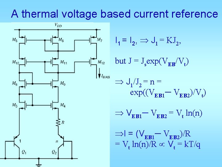
A thermal voltage based current reference I 1 = I 2, J 1 = KJ 2, but J = Jsexp(VEB/Vt) J 1/J 2 = n = exp((VEB 1─ VEB 2)/Vt) VEB 1─ VEB 2 = Vt ln(n) I = (VEB 1─ VEB 2)/R = Vt ln(n)/R Vt = k. T/q

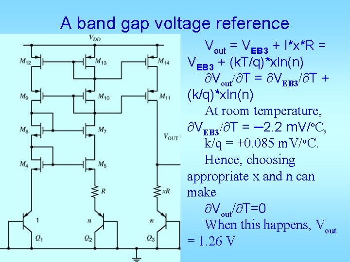
A band gap voltage reference Vout = VEB 3 + I*x*R = VEB 3 + (k. T/q)*xln(n) Vout/ T = VEB 3/ T + (k/q)*xln(n) At room temperature, VEB 3/ T = ─2. 2 m. V/o. C, k/q = +0. 085 m. V/o. C. Hence, choosing appropriate x and n can make Vout/ T=0 When this happens, Vout = 1. 26 V

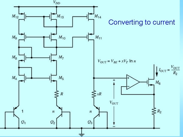
Converting to current
