Radiation effects in devices and technologies Federico Faccio

- Slides: 46

Radiation effects in devices and technologies Federico Faccio CERN – PH dept/ESE group federico. faccio@cern. ch 1

Radiation effects in devices and technologies Outline ü General view ü Total Ionizing Dose (TID) ü Displacement damage ü Single Event Effects l l EIROforum 09 SEU, SET Destructive events Federico Faccio - CERN 2

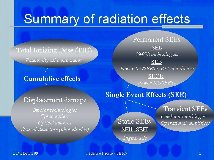
Summary of radiation effects Permanent SEEs SEL Total Ionizing Dose (TID) CMOS technologies Potentially all components SEB Power MOSFETs, BJT and diodes SEGR Cumulative effects Power MOSFETs Displacement damage Bipolar technologies Optocouplers Optical sources Optical detectors (photodiodes) Single Event Effects (SEE) Transient SEEs Static SEEs Combinational logic Operational amplifiers SEU, SEFI Digital ICs EIROforum 09 Federico Faccio - CERN 3

Radiation effects in devices and technologies Outline ü General view ü Total Ionizing Dose (TID) l l TID in CMOS technologies TID in bipolar technologies ü Displacement damage ü Single Event Effects l l EIROforum 09 SEU, SET Destructive events Federico Faccio - CERN 4

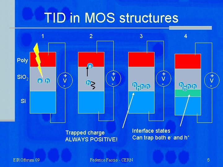
TID in MOS structures 1 2 Poly Si. O 2 4 3 e e h + V - h h Si Trapped charge ALWAYS POSITIVE! EIROforum 09 Interface states Can trap both e- and h+ Federico Faccio - CERN 5

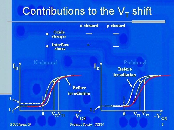
Contributions to the VT shift n-channel p-channel Oxide charges Interface states ID N-channel EIROforum 09 ID P-channel Before irradiation I 2 I 1 + 0 VT 2 VT 1 VGS I 1 Federico Faccio - CERN 0 VT 1 VT 2 -VGS 6

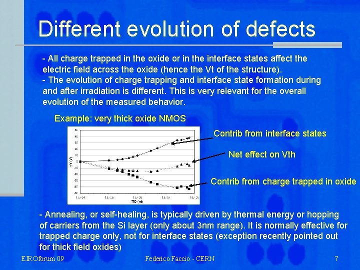
Different evolution of defects - All charge trapped in the oxide or in the interface states affect the electric field across the oxide (hence the Vt of the structure). - The evolution of charge trapping and interface state formation during and after irradiation is different. This is very relevant for the overall evolution of the measured behavior. Example: very thick oxide NMOS Contrib from interface states Net effect on Vth Contrib from charge trapped in oxide - Annealing, or self-healing, is typically driven by thermal energy or hopping of carriers from the Si layer (only about 3 nm range). It is normally effective for trapped charge only, not for interface states (exception recently pointed out for thick field oxides) EIROforum 09 Federico Faccio - CERN 7

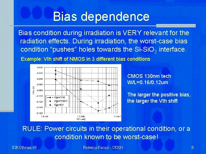
Bias dependence Bias condition during irradiation is VERY relevant for the radiation effects. During irradiation, the worst-case bias condition “pushes” holes towards the Si-Si. O 2 interface. Example: Vth shift of NMOS in 3 different bias conditions CMOS 130 nm tech W/L=0. 16/0. 12 um The larger the positive bias, the larger the Vth shift RULE: Power circuits in their operational condition, or a condition known to be worst-case! EIROforum 09 Federico Faccio - CERN 8

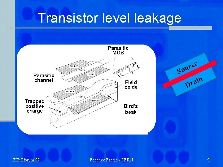
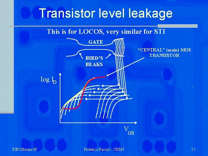
Transistor level leakage Parasitic MOS Parasitic channel Trapped positive charge EIROforum 09 S Field oxide e c r ou n i a r D Bird’s beak Federico Faccio - CERN 9

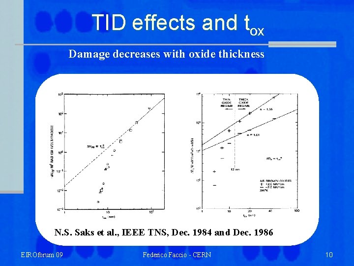
TID effects and tox Damage decreases with oxide thickness Oxide trapped charge Interface states N. S. Saks et al. , IEEE TNS, Dec. 1984 and Dec. 1986 EIROforum 09 Federico Faccio - CERN 10

Transistor level leakage This is for LOCOS, very similar for STI GATE “CENTRAL” (main) MOS TRANSISTOR BIRD’S BEAKS log ID VGS EIROforum 09 Federico Faccio - CERN 11

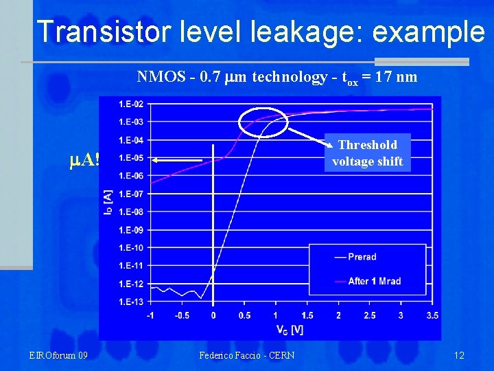
Transistor level leakage: example NMOS - 0. 7 m technology - tox = 17 nm Threshold voltage shift A! EIROforum 09 Federico Faccio - CERN 12

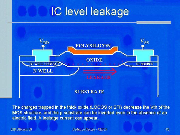
IC level leakage VDD N+ WELL CONTACT VSS POLYSILICON + + + OXIDE + + + N+ SOURCE N WELL LEAKAGE SUBSTRATE The charges trapped in the thick oxide (LOCOS or STI) decrease the Vth of the MOS structure, and the p substrate can be inverted even in the absence of an electric field. A leakage current can appear. EIROforum 09 Federico Faccio - CERN 13

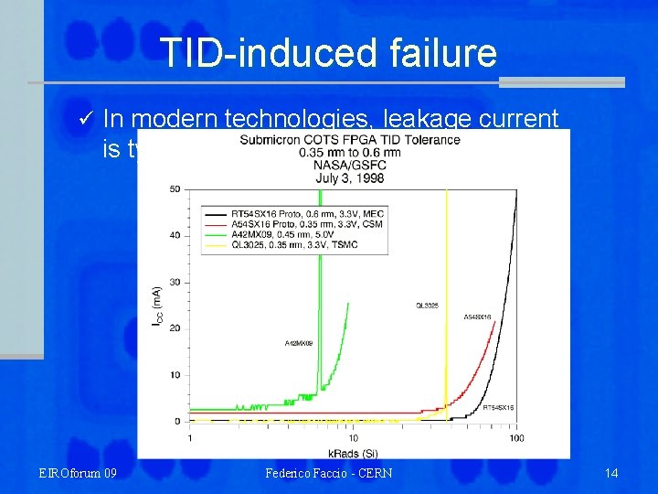
TID-induced failure ü In modern technologies, leakage current is typically the killer EIROforum 09 Federico Faccio - CERN 14

TID in CMOS Summary of the problems ü Main transistor: l l ü Parasitic leakage paths: l l l EIROforum 09 Threshold voltage shift, transconductance and noise degradation Effects get negligible in modern deep submicron (as from 250 -180 nm techs) Source – drain leakage Leakage between devices This are still potentially deleterious – although things looks to be better as from 130 nm techs Federico Faccio - CERN 15

Radiation effects in devices and technologies Outline ü General view ü Total Ionizing Dose (TID) l l TID in CMOS technologies TID in bipolar technologies ü Displacement damage ü Single Event Effects l l EIROforum 09 SEU, SET Destructive events Federico Faccio - CERN 16

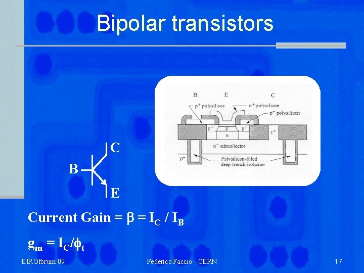
Bipolar transistors C B E Current Gain = = IC / IB gm = IC/ t EIROforum 09 Federico Faccio - CERN 17

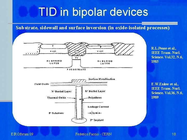
TID in bipolar devices Substrate, sidewall and surface inversion (in oxide-isolated processes) R. L. Pease et al. , IEEE Trans. Nucl. Science. Vol. 32, N. 6, 1985 E. W. Enlow et al. , IEEE Trans. Nucl. Science. Vol. 36, N. 6, 1989 EIROforum 09 Federico Faccio - CERN 18

TID in bipolar devices Gain degradation: Increase of the surface component of the base current R. N. Nowlin et al. , IEEE Trans. Nucl. Science. Vol. 39, N. 6, 1992 EIROforum 09 Federico Faccio - CERN 19

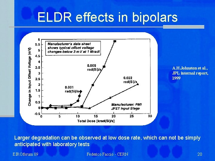
ELDR effects in bipolars A. H. Johnston et al. , JPL internal report, 1999 Larger degradation can be observed at low dose rate, which can not be simply anticipated with laboratory tests EIROforum 09 Federico Faccio - CERN 20

Radiation effects in devices and technologies Outline ü General view ü Total Ionizing Dose (TID) ü Displacement damage ü Single Event Effects l l EIROforum 09 SEU, SET Destructive events Federico Faccio - CERN 21

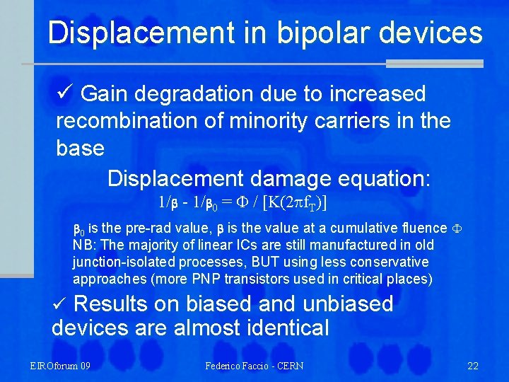
Displacement in bipolar devices ü Gain degradation due to increased recombination of minority carriers in the base Displacement damage equation: 1/ - 1/ 0 = F / [K(2 pf. T)] 0 is the pre-rad value, is the value at a cumulative fluence F NB: The majority of linear ICs are still manufactured in old junction-isolated processes, BUT using less conservative approaches (more PNP transistors used in critical places) Results on biased and unbiased devices are almost identical ü EIROforum 09 Federico Faccio - CERN 22

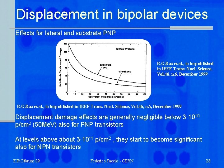
Displacement in bipolar devices Effects for lateral and substrate PNP B. G. Rax et al. , to be published in IEEE Trans. Nucl. Science, Vol. 46, n. 6, December 1999 Displacement damage effects are generally negligible below 3· 1010 p/cm 2 (50 Me. V) also for PNP transistors At levels above about 3· 1011 p/cm 2 , they start to become significant also for NPN transistors EIROforum 09 Federico Faccio - CERN 23

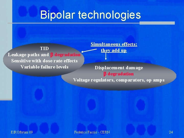
Bipolar technologies TID Leakage paths and degradation Sensitive with dose rate effects Variable failure levels Simultaneous effects: they add up Displacement damage degradation Voltage regulators, comparators, op amps EIROforum 09 Federico Faccio - CERN 24

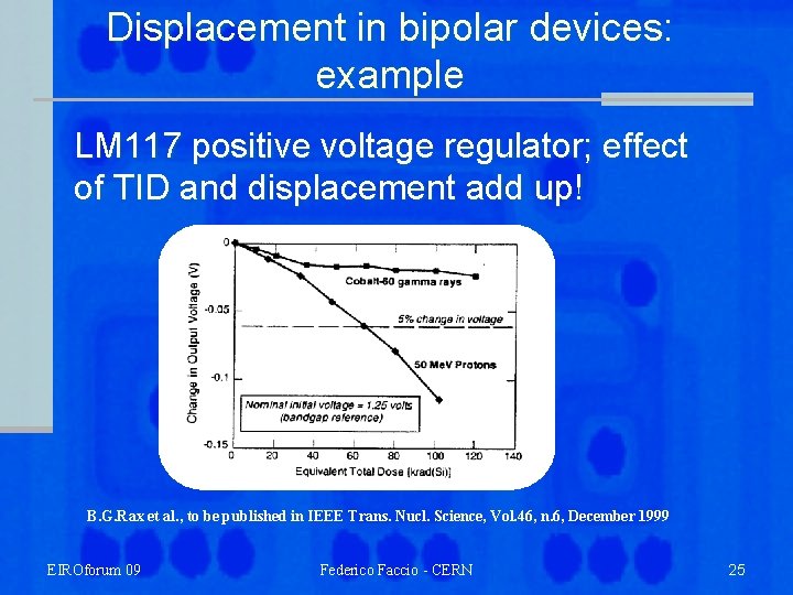
Displacement in bipolar devices: example LM 117 positive voltage regulator; effect of TID and displacement add up! B. G. Rax et al. , to be published in IEEE Trans. Nucl. Science, Vol. 46, n. 6, December 1999 EIROforum 09 Federico Faccio - CERN 25

Radiation effects in devices and technologies Outline ü General view ü Total Ionizing Dose (TID) ü Displacement damage ü Single Event Effects l l EIROforum 09 SEU, SET Destructive events Federico Faccio - CERN 26

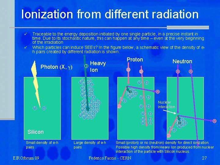
Ionization from different radiation ü ü Traceable to the energy deposition initiated by one single particle, in a precise instant in time. Due to its stochastic nature, this can happen at any time – even at the very beginning of the irradiation Which particles can induce SEEs? In the figure below, a schematic view of the density of eh pairs created by different radiation is shown. Photon (X, g) h e i Proton Heavy Ion hhh eee hh ee h h e e hh hh e eee e hhhhhe ee e hhh h eee e h h h e e p EIROforum 09 n h h n e e Nuclear interaction e e e h e p Large density of e-h pairs n e h ie eee h h hhe he h Silicon Small density of e-h pairs p h h e p Neutron e h eee h h i hhe he n Small (proton) or no (neutron) density for direct ionization. Possible high density from Heavy Ion produced from nuclear interaction of the particle with Silicon nucleus. Federico Faccio - CERN 27

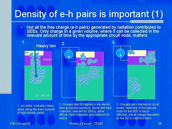
Density of e-h pairs is important (1) Not all the free charge (e-h pairs) generated by radiation contributes to SEEs. Only charge in a given volume, where it can be collected in the relevant amount of time by the appropriate circuit node, matters ü 1. Heavy Ion p+ h e h h e e hh ee Nwell hh ee h e h e hhhh e eeeee hhhhhe ee hhh h eee e h hh eeee h hheeee 3. 2. + h h h e e eee h hhh e e ee ee h hh hhe e ee ee h h hh h e hh hhe h h e h p- silicon 1. Ion strike: ionization takes place along the track (column of high-density pairs) EIROforum 09 2. Charges start to migrate in the electric field across the junctions. Some drift (fast collection, relevant for SEEs), some diffuse (slow collection, less relevant for SEEs) Federico Faccio - CERN + hhhh ee e e e ee eeee h hh hh h h hh hh h 3. Charges are collected at circuit nodes. Note that, if the relevant node for the SEE is the p+ diffusion, not all charge deposited by the ion is collected there. 28

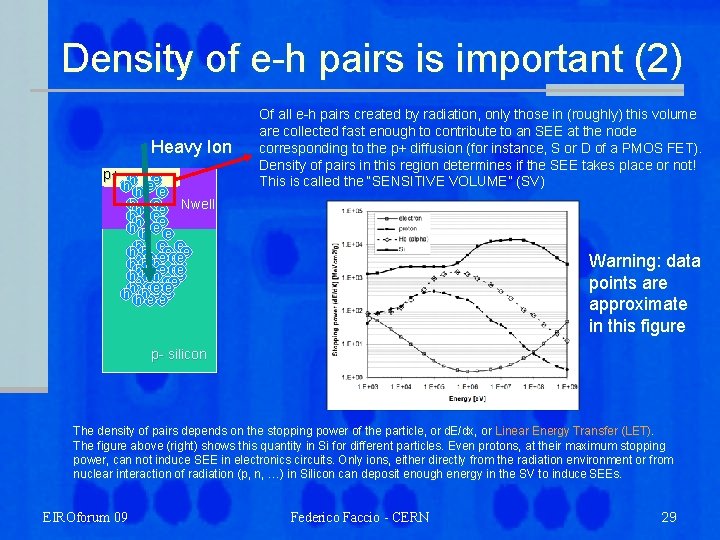
Density of e-h pairs is important (2) Heavy Ion p+ h e h h e e Of all e-h pairs created by radiation, only those in (roughly) this volume are collected fast enough to contribute to an SEE at the node corresponding to the p+ diffusion (for instance, S or D of a PMOS FET). Density of pairs in this region determines if the SEE takes place or not! This is called the “SENSITIVE VOLUME” (SV) h e e Nwell hh e hhh eee hh hh e eee e hhhhhe ee e hhh h eee e h h h e e h hheeee Warning: data points are approximate in this figure p- silicon The density of pairs depends on the stopping power of the particle, or d. E/dx, or Linear Energy Transfer (LET). The figure above (right) shows this quantity in Si for different particles. Even protons, at their maximum stopping power, can not induce SEE in electronics circuits. Only ions, either directly from the radiation environment or from nuclear interaction of radiation (p, n, …) in Silicon can deposit enough energy in the SV to induce SEEs. EIROforum 09 Federico Faccio - CERN 29

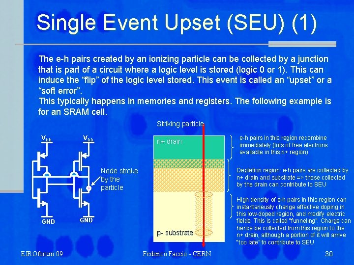
Single Event Upset (SEU) (1) The e-h pairs created by an ionizing particle can be collected by a junction that is part of a circuit where a logic level is stored (logic 0 or 1). This can induce the “flip” of the logic level stored. This event is called an “upset” or a “soft error”. This typically happens in memories and registers. The following example is for an SRAM cell. Striking particle VDD n+ drain Depletion region: e-h pairs are collected by n+ drain and substrate => those collected by the drain can contribute to SEU Node stroke by the particle GND p- substrate EIROforum 09 e-h pairs in this region recombine immediately (lots of free electrons available in this n+ region) Federico Faccio - CERN High density of e-h pairs in this region can instantaneusly change effective doping in this low-doped region, and modify electric fields. This is called “funneling”. Charge can hence be collected from this region to the n+ drain, although a portion of it will arrive “too late” to contribute to SEU 30

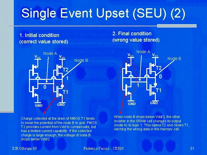
Single Event Upset (SEU) (2) 2. Final condition (wrong value stored) 1. Initial condition (correct value stored) VDD Node A 0 GND VDD VDD Node B T 2 1 0 1 T 1 GND Charge collected at the drain of NMOS T 1 tends to lower the potential of the node B to gnd. PMOS T 2 provides current from Vdd to compensate, but has a limited current capability. If the collected charge is large enough, the voltage of node B drops below Vdd/2 EIROforum 09 Node A T 1 GND When node B drops below Vdd/2, the other inverter in the SRAM cell changes its output (node A) to logic 1. This opens T 2 and closes T 1, latching the wrong data in the memory cell. Federico Faccio - CERN 31

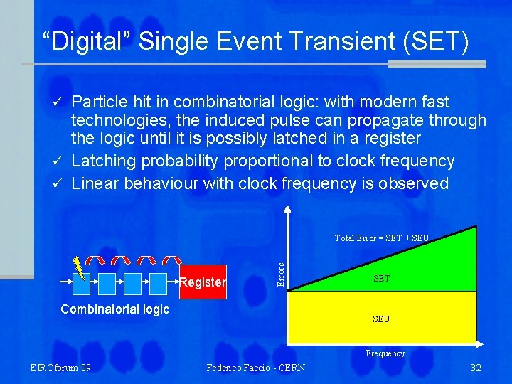
“Digital” Single Event Transient (SET) Particle hit in combinatorial logic: with modern fast technologies, the induced pulse can propagate through the logic until it is possibly latched in a register ü Latching probability proportional to clock frequency ü Linear behaviour with clock frequency is observed ü Register Errors Total Error = SET + SEU Combinatorial logic SET SEU Frequency EIROforum 09 Federico Faccio - CERN 32

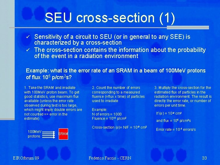
SEU cross-section (1) Sensitivity of a circuit to SEU (or in general to any SEE) is characterized by a cross-section ü The cross-section contains the information about the probability of the event in a radiation environment ü Example: what is the error rate of an SRAM in a beam of 100 Me. V protons of flux 105 p/cm 2 s? 1. Take the SRAM and irradiate with 100 Me. V proton beam. To get good statistics, use maximum flux available (unless the error rate observed during test is too large, which might imply double errors are not counted => error in the estimate) 2. Count the number of errors corresponding to a measured fluence (=flux x time) of particles used to irradiate Example: N of errors = 1000 Fluence = 1012 p/cm 2 Cross-section (s)= N/F = 10 -9 cm 2 100 Me. V protons EIROforum 09 3. Multiply the cross-section for the estimated flux of particles in the radiation environment. The result is directly the error rate, or number of errors per unit time. If (s) = 10 -9 cm 2 and flux = 105 p/cm 2 s Error rate = 10 -4 errors/s SRAM Federico Faccio - CERN 33

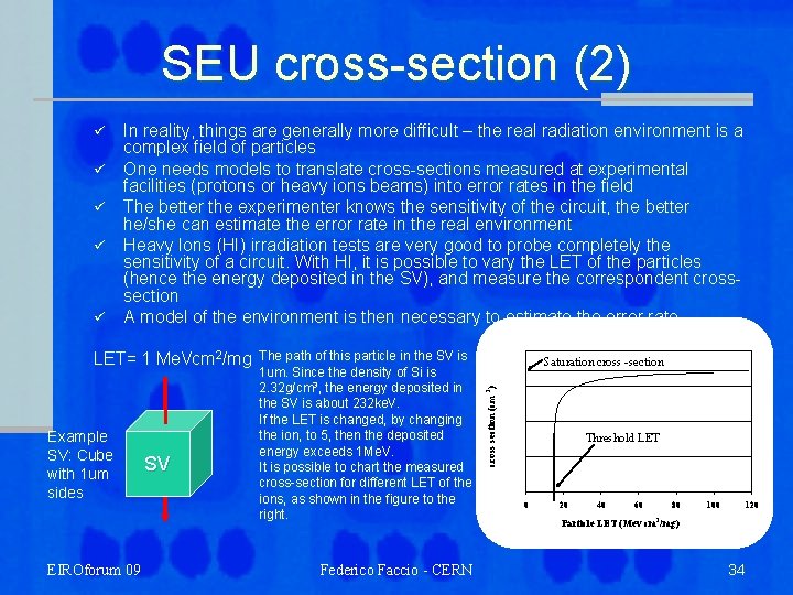
SEU cross-section (2) ü ü ü LET= 1 Me. Vcm 2/mg Example SV: Cube with 1 um sides EIROforum 09 SV The path of this particle in the SV is 1 um. Since the density of Si is 2. 32 g/cm 3, the energy deposited in the SV is about 232 ke. V. If the LET is changed, by changing the ion, to 5, then the deposited energy exceeds 1 Me. V. It is possible to chart the measured cross-section for different LET of the ions, as shown in the figure to the right. Federico Faccio - CERN Saturation cross -section 2 ü In reality, things are generally more difficult – the real radiation environment is a complex field of particles One needs models to translate cross-sections measured at experimental facilities (protons or heavy ions beams) into error rates in the field The better the experimenter knows the sensitivity of the circuit, the better he/she can estimate the error rate in the real environment Heavy Ions (HI) irradiation tests are very good to probe completely the sensitivity of a circuit. With HI, it is possible to vary the LET of the particles (hence the energy deposited in the SV), and measure the correspondent crosssection A model of the environment is then necessary to estimate the error rate cross section (cm ) ü Threshold LET 0 20 40 60 2 80 100 120 2 Particle LET (Mev cm(Mev /mg)cm or /mg) proton energy (Me. V) LET 34

Radiation effects in devices and technologies Outline ü General view ü Total Ionizing Dose (TID) ü Displacement damage ü Single Event Effects l l EIROforum 09 SEU, SET Destructive events Federico Faccio - CERN 35

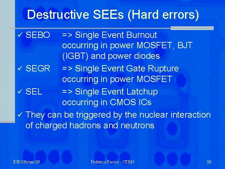
Destructive SEEs (Hard errors) => Single Event Burnout occurring in power MOSFET, BJT (IGBT) and power diodes ü SEGR => Single Event Gate Rupture occurring in power MOSFET ü SEL => Single Event Latchup occurring in CMOS ICs ü They can be triggered by the nuclear interaction of charged hadrons and neutrons ü SEBO EIROforum 09 Federico Faccio - CERN 36

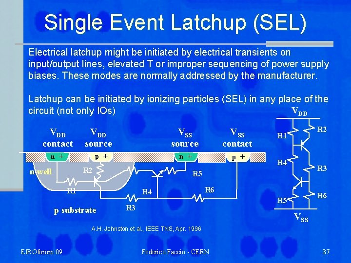
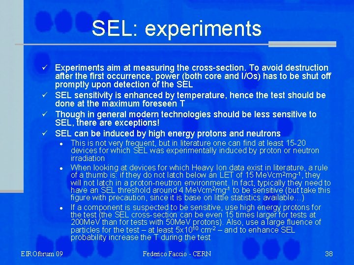
Single Event Latchup (SEL) Electrical latchup might be initiated by electrical transients on input/output lines, elevated T or improper sequencing of power supply biases. These modes are normally addressed by the manufacturer. Latchup can be initiated by ionizing particles (SEL) in any place of the VDD circuit (not only IOs) VDD contact VDD source n + p + R 2 n well VSS source VSS contact n + p + R 4 R 3 R 5 R 1 R 4 p substrate R 2 R 1 R 6 R 5 R 3 VSS A. H. Johnston et al. , IEEE TNS, Apr. 1996 EIROforum 09 Federico Faccio - CERN 37

SEL: experiments ü ü Experiments aim at measuring the cross-section. To avoid destruction after the first occurrence, power (both core and I/Os) has to be shut off promptly upon detection of the SEL sensitivity is enhanced by temperature, hence the test should be done at the maximum foreseen T Though in general modern technologies should be less sensitive to SEL, there are exceptions! SEL can be induced by high energy protons and neutrons l l l EIROforum 09 This is not very frequent, but in literature one can find at least 15 -20 devices for which SEL was experimentally induced by proton or neutron irradiation When looking at devices for which Heavy Ion data exist in literature, a rule of a thumb is: if they do not latch below an LET of 15 Me. Vcm 2 mg-1, they will not latch in a proton-neutron environment. In fact, typically they need to have an SEL threshold around 4 Me. Vcm 2 mg-1 to be sensitive (but take this figure with precaution, since it is base on little statistics available…) If a component is suspected to be sensitive, use high energy protons for the test (the SEL cross-section can be even 15 times larger for tests at 200 Me. V than for tests with 50 Me. V protons). Also, use a large fluence of particles for the test – at least 5 x 1010 cm-2 – and to enhance SEL probability increase the T during the test Federico Faccio - CERN 38

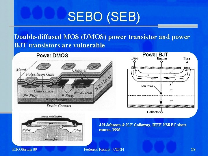
SEBO (SEB) Double-diffused MOS (DMOS) power transistor and power BJT transistors are vulnerable Power BJT Power DMOS J. H. Johnson & K. F. Galloway, IEEE NSREC short course, 1996 EIROforum 09 Federico Faccio - CERN 39

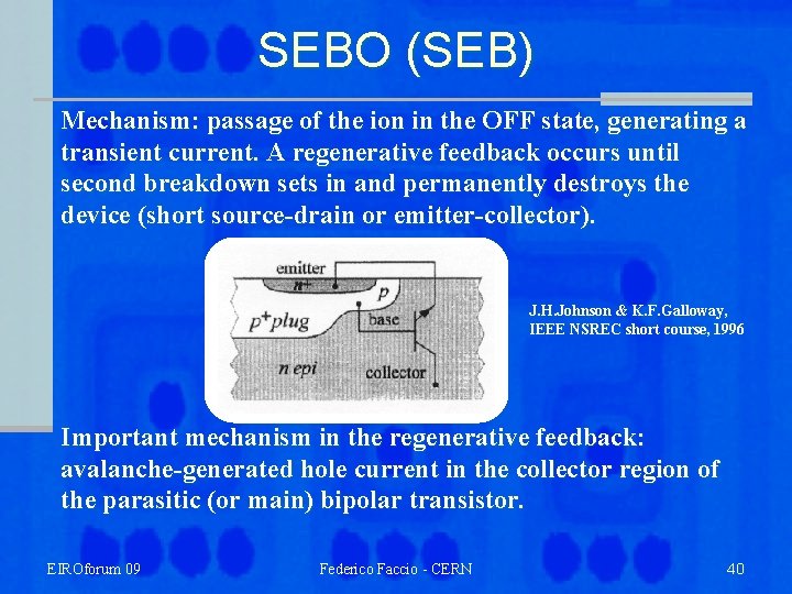
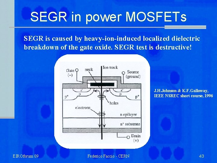
SEBO (SEB) Mechanism: passage of the ion in the OFF state, generating a transient current. A regenerative feedback occurs until second breakdown sets in and permanently destroys the device (short source-drain or emitter-collector). J. H. Johnson & K. F. Galloway, IEEE NSREC short course, 1996 Important mechanism in the regenerative feedback: avalanche-generated hole current in the collector region of the parasitic (or main) bipolar transistor. EIROforum 09 Federico Faccio - CERN 40

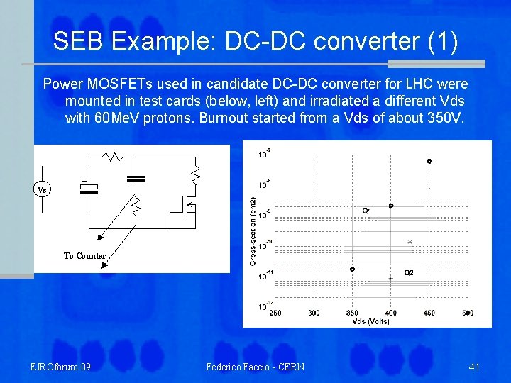
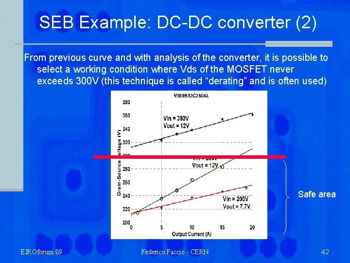
SEB Example: DC-DC converter (1) Power MOSFETs used in candidate DC-DC converter for LHC were mounted in test cards (below, left) and irradiated a different Vds with 60 Me. V protons. Burnout started from a Vds of about 350 V. Vs + To Counter EIROforum 09 Federico Faccio - CERN 41

SEB Example: DC-DC converter (2) From previous curve and with analysis of the converter, it is possible to select a working condition where Vds of the MOSFET never exceeds 300 V (this technique is called “derating” and is often used) Safe area EIROforum 09 Federico Faccio - CERN 42

SEGR in power MOSFETs SEGR is caused by heavy-ion-induced localized dielectric breakdown of the gate oxide. SEGR test is destructive! J. H. Johnson & K. F. Galloway, IEEE NSREC short course, 1996 EIROforum 09 Federico Faccio - CERN 43

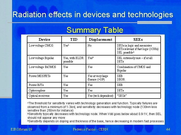
Radiation effects in devices and technologies Summary Table Device TID Displacement SEEs Low voltage CMOS Yes 1 No SEUs in logic and memories SETs relevant if fast logic (1 GHz) SEL possible 2 Low voltage Bipolar Yes, with ELDR possible Yes 3 SEL extremely rare – if at all SETs Low voltage Bi. CMOS Yes Combination of CMOS and Bipolar Power MOSFETs Yes at very large fluence (>10 f) SEB SEGR Power BJTs Yes SEB Optocouplers Yes SETs Optical receivers Yes (tech dependent) “SEUs” 1 The threshold for sensitivity varies with technology generation and function. Typically failures are observed from a minimum of 1 -3 krd, and sensitivity decreases with technology node (130 nm less sensitive than 250 nm for instance) 2 Sensitivity typically decreases with technology node. When Vdd goes below about 0. 8 -1 V, then SEL should not appear any more 3 Sensitivity depends on doping and thickness of the base, hence decreasing in modern fast processes EIROforum 09 Federico Faccio - CERN 44

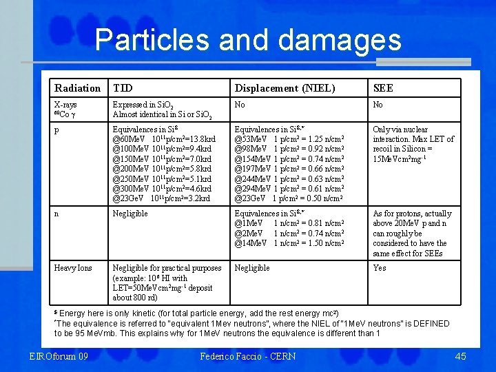
Particles and damages Radiation TID Displacement (NIEL) SEE X-rays 60 Co g Expressed in Si. O 2 Almost identical in Si or Si. O 2 No No p Equivalences in Si $ @60 Me. V 1011 p/cm 2=13. 8 krd @100 Me. V 1011 p/cm 2=9. 4 krd @150 Me. V 1011 p/cm 2=7. 0 krd @200 Me. V 1011 p/cm 2=5. 8 krd @250 Me. V 1011 p/cm 2=5. 1 krd @300 Me. V 1011 p/cm 2=4. 6 krd @23 Ge. V 1011 p/cm 2=3. 2 krd Equivalences in Si $, * @53 Me. V 1 p/cm 2 = 1. 25 n/cm 2 @98 Me. V 1 p/cm 2 = 0. 92 n/cm 2 @154 Me. V 1 p/cm 2 = 0. 74 n/cm 2 @197 Me. V 1 p/cm 2 = 0. 66 n/cm 2 @244 Me. V 1 p/cm 2 = 0. 63 n/cm 2 @294 Me. V 1 p/cm 2 = 0. 61 n/cm 2 @23 Ge. V 1 p/cm 2 = 0. 50 n/cm 2 Only via nuclear interaction. Max LET of recoil in Silicon = 15 Me. Vcm 2 mg-1 n Negligible Equivalences in Si $, * @1 Me. V 1 n/cm 2 = 0. 81 n/cm 2 @2 Me. V 1 n/cm 2 = 0. 74 n/cm 2 @14 Me. V 1 n/cm 2 = 1. 50 n/cm 2 As for protons, actually above 20 Me. V p and n can roughly be considered to have the same effect for SEEs Heavy Ions Negligible for practical purposes (example: 106 HI with LET=50 Me. Vcm 2 mg-1 deposit about 800 rd) Negligible Yes $ Energy here is only kinetic (for total particle energy, add the rest energy mc 2) *The equivalence is referred to “equivalent 1 Mev neutrons”, where the NIEL of “ 1 Me. V neutrons” is DEFINED to be 95 Me. Vmb. This explains why for 1 Me. V neutrons the equivalence is different than 1 EIROforum 09 Federico Faccio - CERN 45

To study further… ü General material on radiation effects: l l The best source is the “archive of Radiation Effects Short Course Notebooks, 19802006” collecting the courses given at the IEEE NSREC conference (CD sold by IEEE) “Classic” books on the subject • • l Recent Books with good overview of all effects: • • l ü “Ionizing radiation effects in MOS devices and circuits”, edited by T. Ma and P. Dressendorfer, published by Wiley (2001), ISBN 978 -0471848936 “Handbook of radiation effects”, by A. Holmes-Siedle and L. Adams, published by Oxford University Press (2002), ISBN 978 -0198507338 “Radiation effects on Embedded Systems”, edited by R. Velazco, P. Fouillat, R. Reis, published by Springer (2007), ISBN 978 -1 -4020 -5645 -1 “Radiation effects and soft errors in integrated circuits and electronic devices”, edited by R. Schrimpf and D. Fleetwood, published by World Scientific (2004), ISBN 981 -238 -940 -7 Best papers from the Nuclear and Space Radiation Effects Conference (NSREC) are published yearly in the IEEE TNS in the december special Issue Specialized conferences: l l EIROforum 09 NSREC in the US, yearly in July RADECs in Europe, conference (1 week) or workshop (2 -3 days) every year in September Federico Faccio - CERN 46