MOSFET Sangeeta Sinha Physics Department A N College


 ID – current flows from")

 Graph between ID and VDS at different constant value")

 • Graph between ID and VGS at constant VDS")


- Slides: 18
MOSFET ----Sangeeta Sinha Physics Department A N College
• • • Metal Oxide Field Effect Transistor -- MOSFET Insulated Gate Field Effect Transistor – IGFET Active Semiconductor Device • Two types – • • • 1. Enhancement MOSFET ( i) n- channel (ii) p-channel It has no channel between source and drain initially • • 2. Depletion MOSFET (i) n- channel (ii) p- channel • It has channel between source and drain from beginning •
Enhancement Type MOSFET Construction- n-channel Lightly doped p-type semiconductor bar – Substrate or Body
• • Two n-type well heavily doped- diffused into p-type semiconductor bar Two p-n junction – two depletion region of same width Source – one n-type well Drain - other n-type well Gate - A thin layer of Si. O 2 deposited between wells Metallic layer – over n-well , Si. O 2 layer and the bottom of bar Channel - no No current flow due to two p-n junction
Making a Channel • G and S connected to a battery
• The free electrons of p type accumulate near the Si. O 2 layer – behaves like di electric between plates of capacitor
Working When VGS = 0, it is normally off • When VGS – low , Electron accumulation less • VGS - increased , more electrons accumulation between n type wells • Hence, it behaves n type between wells inside the p type body – channel made
At certain voltage of VGS - channel is made – Threshold Voltage ( VT ) When VGS ≥ VT – Channel VGS < VT – no channel By increasing VGS , more electrons accumulation – more thick channel – behaves like n-type Inversion Process – p type material changed into n type material and vice-versa There is depletion layer around the channel Two p-n junction one between drain and body second between body and source
Now source and drain is connected by a battery(VDS) ID – current flows from drain to source •
• • ID increased with VDS Depletion layer thick at D side. Channel – narrow Channel becomes narrower with increased VDS ID not increased with VDS – saturated This value of ID – saturation Current Condition – Pinch off Value of VDS – saturation voltage – VDSat = VGS – VT
Drain Characteristic ( Output ) Graph between ID and VDS at different constant value of VGS
ID increases with VDS • At its certain value ID constant – independent of VDSat increasing with increased value of VGS Three region – 1. Active Region -The width of channel is changed with VGS at fixed value of VDS In This region MOSFET is operated as voltage controll resister 2. Cut- off Region – VGS < VT – MOSFET in off condition 3. Saturation Region. ID constant -- VDS ≥ VGS – VT
Transfer Characteristic ( Input ) • Graph between ID and VGS at constant VDS • For low value of VGS , no ID • Relation between ID and VGS expressed as • ID = K( VGS – VT )2 where K is device constant.
P - Channel MOSFET
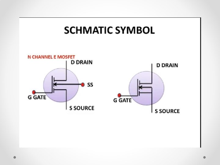
SYMBOL
• Drain Characteristic • VGS negative • More negative VGS more ID
Transfer Characteristic • It is mirror image of n – channel curve