Memory System UnitIV 12252021 Unit4 Memory System 1
- Slides: 28

Memory System Unit-IV 12/25/2021 Unit-4 : Memory System 1

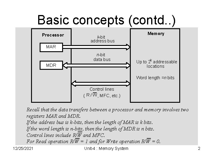
Basic concepts (contd. . ) Processor k-bit address bus Memory MAR n-bit data bus MDR Up to 2 k addressable locations Word length =n bits Control lines ( R / W , MFC, etc. ) Recall that the data transfers between a processor and memory involves two registers MAR and MDR. If the address bus is k-bits, then the length of MAR is k bits. If the word length is n-bits, then the length of MDR is n bits. Control lines include R/W and MFC. For Read operation R/W = 1 and for Write operation R/W = 0. 12/25/2021 Unit-4 : Memory System 2

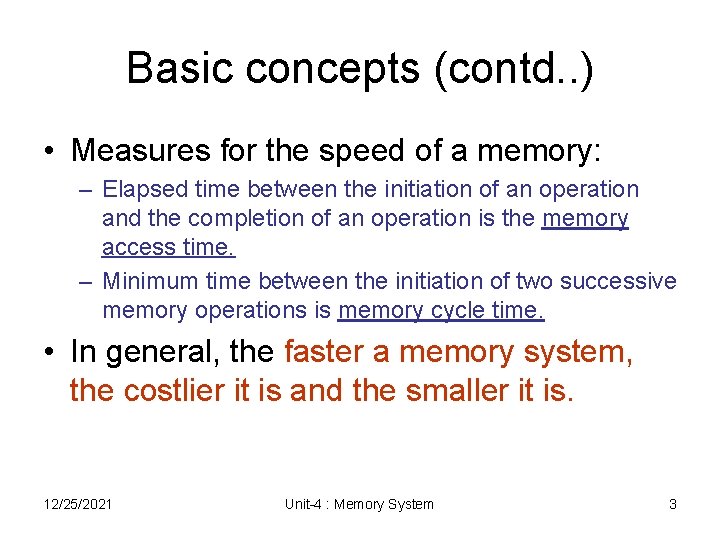
Basic concepts (contd. . ) • Measures for the speed of a memory: – Elapsed time between the initiation of an operation and the completion of an operation is the memory access time. – Minimum time between the initiation of two successive memory operations is memory cycle time. • In general, the faster a memory system, the costlier it is and the smaller it is. 12/25/2021 Unit-4 : Memory System 3

Basic concepts (contd. . ) • An important design issue is to provide a computer system with as large and fast a memory as possible, within a given cost target. • Several techniques to increase the effective size and speed of the memory: – Cache memory (to increase the effective speed). – Virtual memory (to increase the effective size). 12/25/2021 Unit-4 : Memory System 4

Semiconductor RAM memories • Random Access Memory (RAM) memory unit is a unit where any location can be addressed in a fixed amount of time, independent of the location’s address. 12/25/2021 Unit-4 : Memory System 5

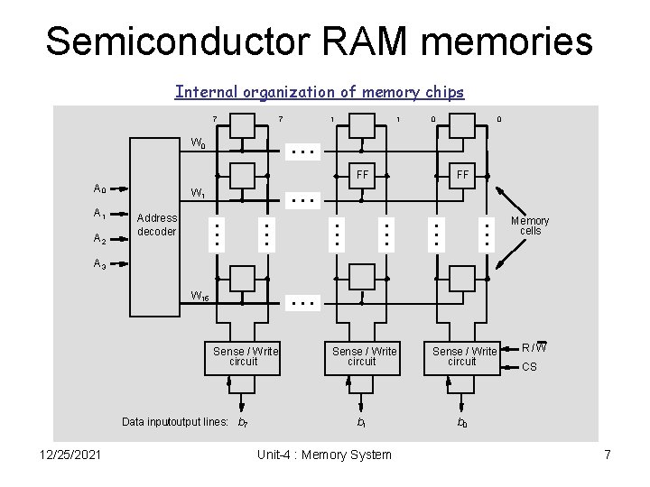
Semiconductor RAM memories • Internal organization of memory chips: – – Each memory cell can hold one bit of information. Memory cells are organized in the form of an array. One row is one memory word. All cells of a row are connected to a common line, known as the “word line”. – Word line is connected to the address decoder. – Sense/write circuits are connected to the data input/output lines of the memory chip. 12/25/2021 Unit-4 : Memory System 6

Semiconductor RAM memories Internal organization of memory chips 7 7 1 1 0 0 W 0 • • • FF A 0 A 2 Address decoder • • • A 1 W 1 FF • • • • • Memory cells A 3 • • • W 15 Sense / Write circuit Data input/output lines: b 7 12/25/2021 Sense / Write circuit b 1 Unit-4 : Memory System Sense / Write circuit R/W CS b 0 7

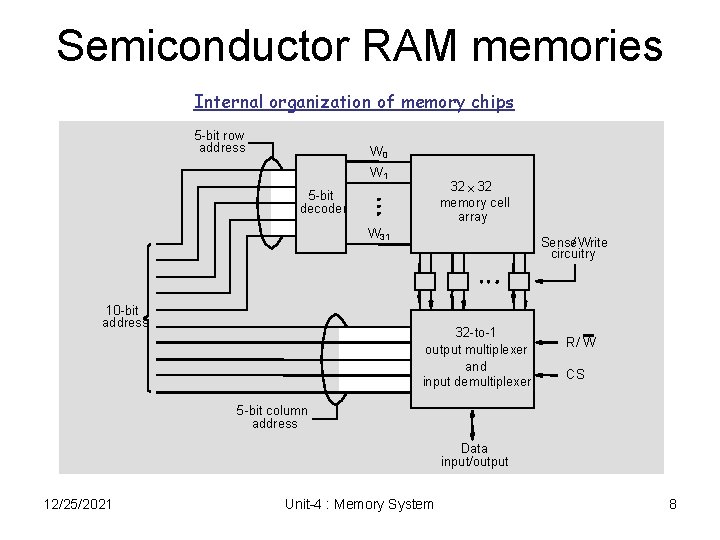
Semiconductor RAM memories Internal organization of memory chips 5 -bit row address W 0 W 1 32 ´ 32 memory cell array 5 -bit decoder W 31 10 -bit address Sense/Write circuitry 32 -to-1 output multiplexer and input demultiplexer R/ W CS 5 -bit column address Data input/output 12/25/2021 Unit-4 : Memory System 8

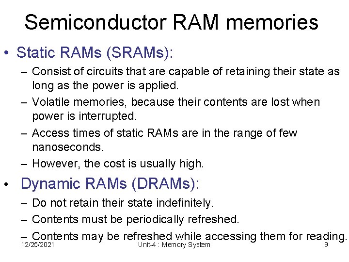
Semiconductor RAM memories • Static RAMs (SRAMs): – Consist of circuits that are capable of retaining their state as long as the power is applied. – Volatile memories, because their contents are lost when power is interrupted. – Access times of static RAMs are in the range of few nanoseconds. – However, the cost is usually high. • Dynamic RAMs (DRAMs): – Do not retain their state indefinitely. – Contents must be periodically refreshed. – Contents may be refreshed while accessing them for reading. 12/25/2021 Unit-4 : Memory System 9

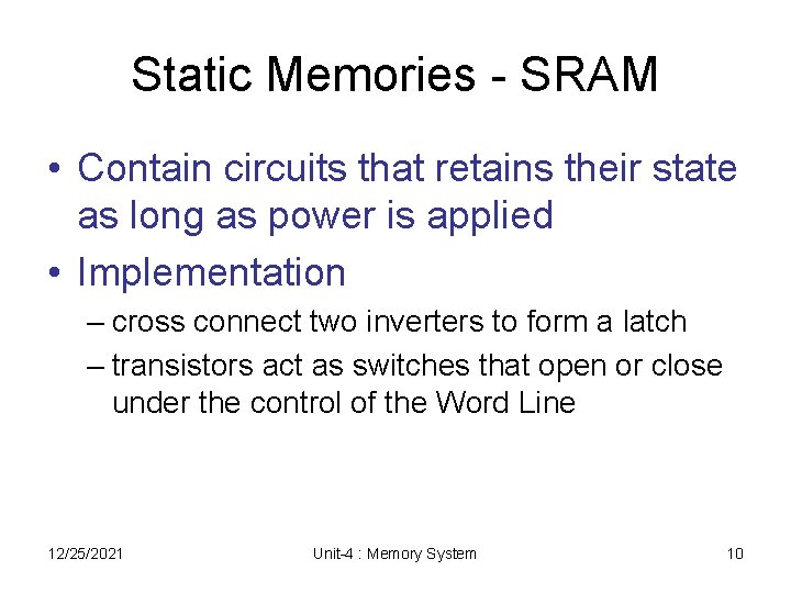
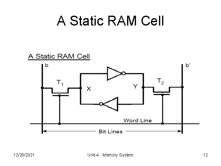
Static Memories - SRAM • Contain circuits that retains their state as long as power is applied • Implementation – cross connect two inverters to form a latch – transistors act as switches that open or close under the control of the Word Line 12/25/2021 Unit-4 : Memory System 10

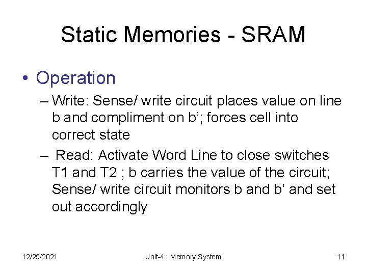
Static Memories - SRAM • Operation – Write: Sense/ write circuit places value on line b and compliment on b’; forces cell into correct state – Read: Activate Word Line to close switches T 1 and T 2 ; b carries the value of the circuit; Sense/ write circuit monitors b and b’ and set out accordingly 12/25/2021 Unit-4 : Memory System 11

A Static RAM Cell 12/25/2021 Unit-4 : Memory System 12

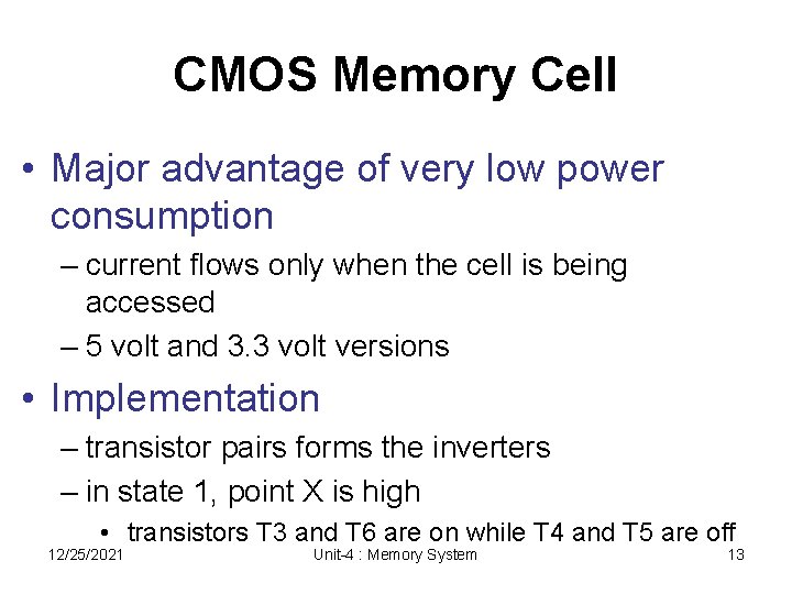
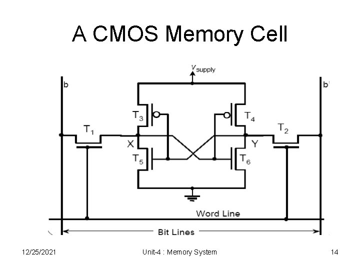
CMOS Memory Cell • Major advantage of very low power consumption – current flows only when the cell is being accessed – 5 volt and 3. 3 volt versions • Implementation – transistor pairs forms the inverters – in state 1, point X is high • transistors T 3 and T 6 are on while T 4 and T 5 are off 12/25/2021 Unit-4 : Memory System 13

A CMOS Memory Cell 12/25/2021 Unit-4 : Memory System 14

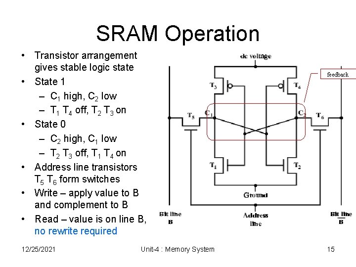
SRAM Operation • Transistor arrangement gives stable logic state • State 1 – C 1 high, C 2 low – T 1 T 4 off, T 2 T 3 on • State 0 – C 2 high, C 1 low – T 2 T 3 off, T 1 T 4 on • Address line transistors T 5 T 6 form switches • Write – apply value to B and complement to B • Read – value is on line B, no rewrite required 12/25/2021 Unit-4 : Memory System feedback 15

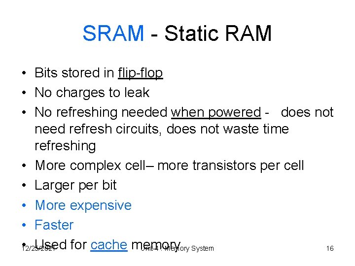
SRAM - Static RAM • Bits stored in flip-flop • No charges to leak • No refreshing needed when powered - does not need refresh circuits, does not waste time refreshing • More complex cell– more transistors per cell • Larger per bit • More expensive • Faster • Used for cache memory 12/25/2021 Unit-4 : Memory System 16

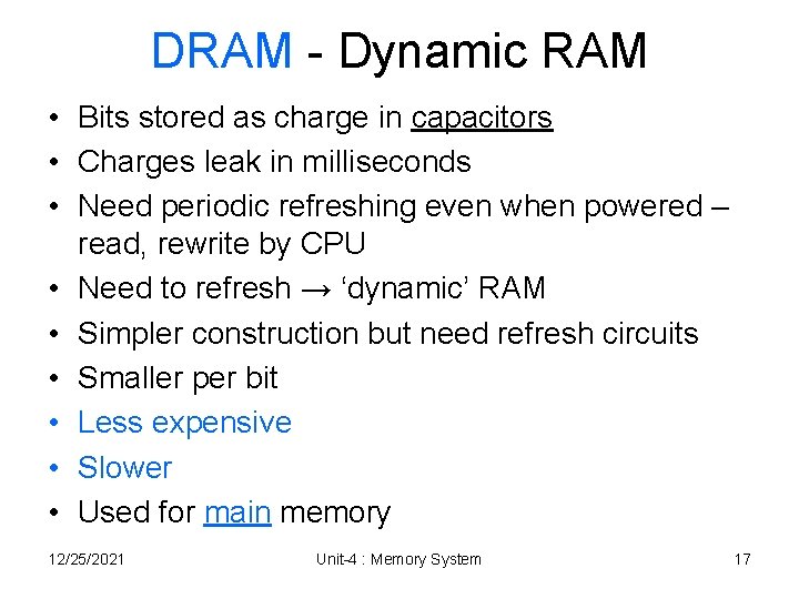
DRAM - Dynamic RAM • Bits stored as charge in capacitors • Charges leak in milliseconds • Need periodic refreshing even when powered – read, rewrite by CPU • Need to refresh → ‘dynamic’ RAM • Simpler construction but need refresh circuits • Smaller per bit • Less expensive • Slower • Used for main memory 12/25/2021 Unit-4 : Memory System 17

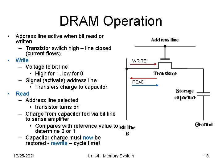
DRAM Operation • • • Address line active when bit read or written – Transistor switch high – line closed (current flows) Write – Voltage to bit line • High for 1, low for 0 – Signal (activate) address line • Transfers charge to capacitor Read – Address line selected • transistor turns on – Charge from capacitor fed via bit line to sense amplifier • Compares with reference value to determine 0 or 1 – Capacitor charge must now be restored - rewrite – cycle time! 12/25/2021 WRITE READ Unit-4 : Memory System 18

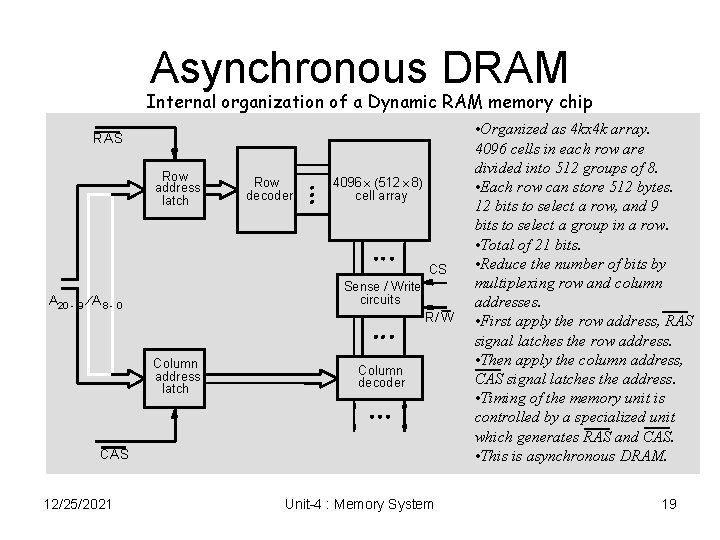
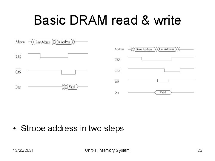
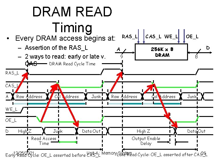
Asynchronous DRAM Internal organization of a Dynamic RAM memory chip RA S Row address latch Row decoder 4096´ (512 ´ 8) cell array CS A 20 - 9 ¤ A 8 - Sense / Write circuits 0 R/ W Column address latch Column decoder CA S 12/25/2021 Unit-4 : Memory System • Organized as 4 kx 4 k array. 4096 cells in each row are divided into 512 groups of 8. • Each row can store 512 bytes. 12 bits to select a row, and 9 bits to select a group in a row. • Total of 21 bits. • Reduce the number of bits by multiplexing row and column addresses. • First apply the row address, RAS signal latches the row address. • Then apply the column address, CAS signal latches the address. • Timing of the memory unit is controlled by a specialized unit which generates RAS and CAS. • This is asynchronous DRAM. 19

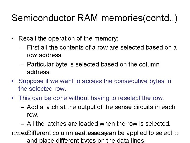
Semiconductor RAM memories(contd. . ) • Recall the operation of the memory: – First all the contents of a row are selected based on a row address. – Particular byte is selected based on the column address. • Suppose if we want to access the consecutive bytes in the selected row. • This can be done without having to reselect the row. – Add a latch at the output of the sense circuits in each row. – All the latches are loaded when the row is selected. 12/25/2021 Unit-4 : Memory System – Different column addresses can be applied to select 20 and place different bytes on the data lines.

Semiconductor RAM memories(contd. . ) • Consecutive sequence of column addresses can be applied under the control signal CAS, without reselecting the row. – Allows a block of data to be transferred at a much faster rate than random accesses. – A small collection/group of bytes is usually referred to as a block. • This transfer capability is referred to as the fast page mode feature. 12/25/2021 Unit-4 : Memory System 21

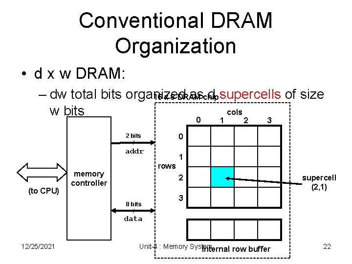
Conventional DRAM Organization • d x w DRAM: – dw total bits organized aschip d supercells of size 16 x 8 DRAM cols w bits 0 2 bits / 2 3 0 addr (to CPU) 1 1 rows memory controller 2 8 bits / supercell (2, 1) 3 data 12/25/2021 Unit-4 : Memory System internal row buffer 22

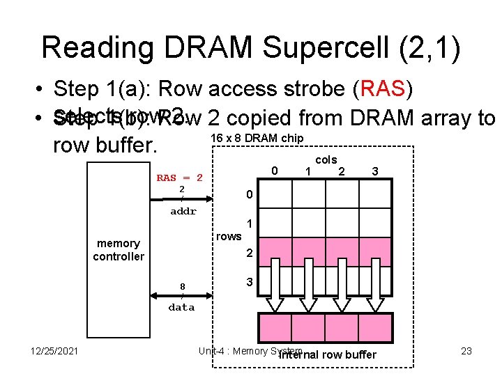
Reading DRAM Supercell (2, 1) • Step 1(a): Row access strobe (RAS) selects row. Row 2. 2 copied from DRAM array to • Step 1(b): 16 x 8 DRAM chip row buffer. 0 RAS = 2 2 / 1 cols 2 3 0 addr 1 rows memory controller 2 8 / 3 data 12/25/2021 Unit-4 : Memory System internal row buffer 23

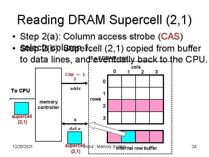
Reading DRAM Supercell (2, 1) • Step 2(a): Column access strobe (CAS) selects column 1. (2, 1) copied from buffer • Step 2(b): Supercell x 8 DRAM chip to data lines, and 16 eventually back to the CPU. 0 CAS = 1 2 / 2 3 0 addr To CPU 1 rows memory controller supercell (2, 1) 1 cols 2 8 / 3 data 12/25/2021 supercell Unit-4 : Memory System internal row buffer (2, 1) 24

Basic DRAM read & write • Strobe address in two steps 12/25/2021 Unit-4 : Memory System 25

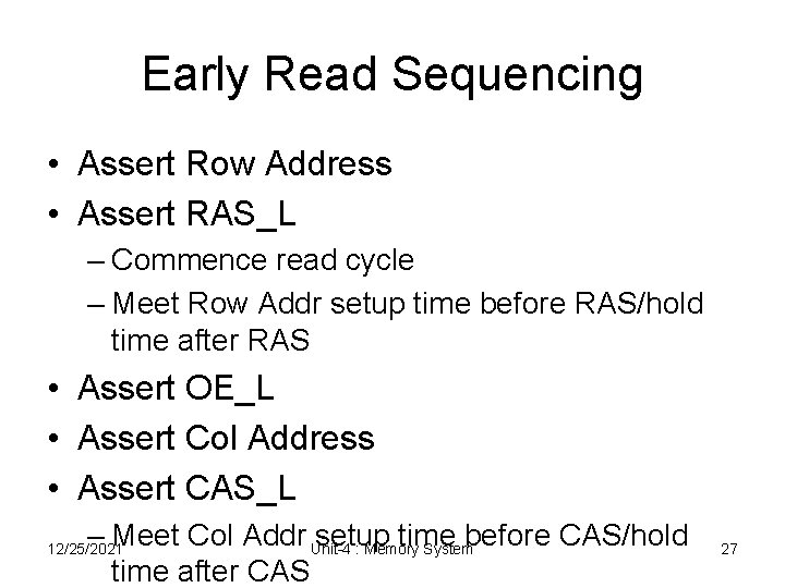
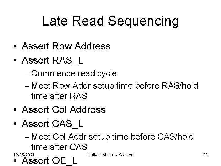
DRAM READ Timing RAS_L • Every DRAM access begins at: – Assertion of the RAS_L – 2 ways to read: early or late v. DRAM Read Cycle Time CAS_L WE_L A 256 K x 8 DRAM 9 OE_L D 8 RAS_L CAS_L A Row Address Col Address Junk WE_L OE_L D High Z Junk Read Access Time Data Out High Z Data Output Enable Delay 12/25/2021 Unit-4 : Memory. Late System 26 Read Cycle: OE_L asserted after CAS_L Early Read Cycle: OE_L asserted before CAS_L

Early Read Sequencing • Assert Row Address • Assert RAS_L – Commence read cycle – Meet Row Addr setup time before RAS/hold time after RAS • Assert OE_L • Assert Col Address • Assert CAS_L – Meet Col Addr Unit-4 setup time before CAS/hold : Memory System time after CAS 12/25/2021 27

Late Read Sequencing • Assert Row Address • Assert RAS_L – Commence read cycle – Meet Row Addr setup time before RAS/hold time after RAS • Assert Col Address • Assert CAS_L – Meet Col Addr setup time before CAS/hold time after CAS 12/25/2021 • Assert OE_L Unit-4 : Memory System 28