Low Noise Front End ASIC with Current Mode
- Slides: 28

Low Noise Front End ASIC with Current Mode Active Cooled Termination for the Upgrade of the LHCb Calorimeter E. Picatoste, C. Abellan, O. Duarte, L. Garrido, D. Gascon, J. Lefrançois, E. Grauges, F. Machefert, X. Vilasis Universitat de Barcelona Institut de Ciències del Cosmos ICC-UB TWEPP-11 – 26 -30 September 2011 – Vienna, Austria

Outline 1. 2. 3. 4. 5. Introduction Channel Architecture First prototype Second prototype Summary 27 th September 2011 TWEPP-11 2

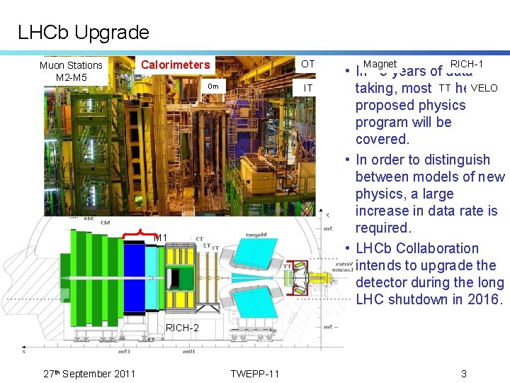
LHCb Upgrade Muon Stations M 2 -M 5 OT Calorimeters 10 m -5 m 5 m 0 m y IT M 1 Magnet RICH-1 • In ~5 years of data TT the. VELO taking, most of proposed physics program will be covered. • In order to distinguish between models of new physics, a large increase in data rate is required. • LHCb Collaboration intends to upgrade the detector during the long LHC shutdown in 2016. RICH-2 27 th September 2011 TWEPP-11 3

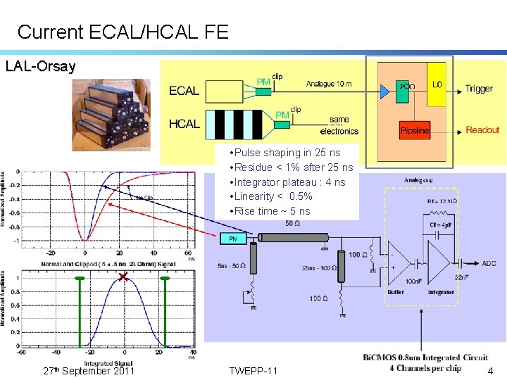
Current ECAL/HCAL FE LAL-Orsay • Pulse shaping in 25 ns • Residue < 1% after 25 ns • Integrator plateau : 4 ns • Linearity < 0. 5% • Rise time ~ 5 ns 27 th September 2011 TWEPP-11 4

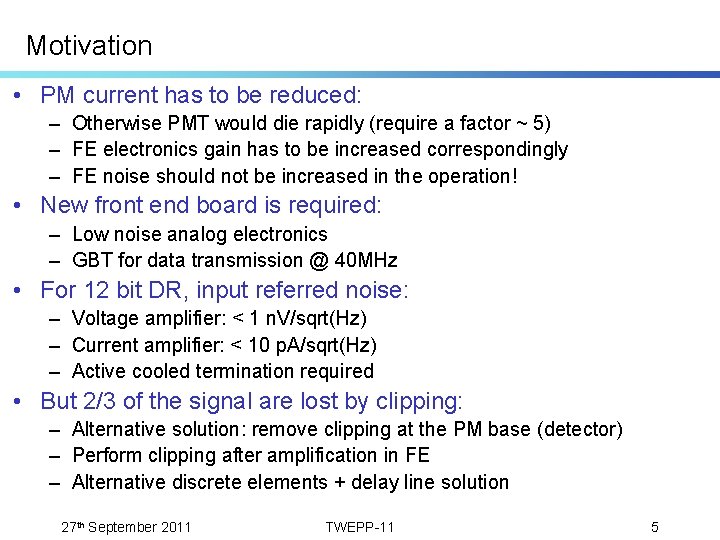
Motivation • PM current has to be reduced: – Otherwise PMT would die rapidly (require a factor ~ 5) – FE electronics gain has to be increased correspondingly – FE noise should not be increased in the operation! • New front end board is required: – Low noise analog electronics – GBT for data transmission @ 40 MHz • For 12 bit DR, input referred noise: – Voltage amplifier: < 1 n. V/sqrt(Hz) – Current amplifier: < 10 p. A/sqrt(Hz) – Active cooled termination required • But 2/3 of the signal are lost by clipping: – Alternative solution: remove clipping at the PM base (detector) – Perform clipping after amplification in FE – Alternative discrete elements + delay line solution 27 th September 2011 TWEPP-11 5

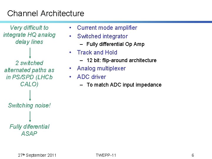
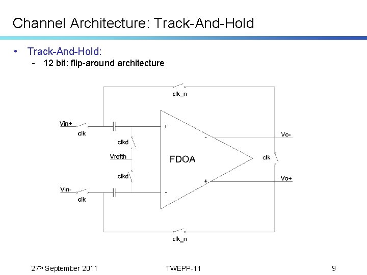
Channel Architecture Very difficult to integrate HQ analog delay lines • Current mode amplifier • Switched integrator – Fully differential Op Amp • Track and Hold 2 switched alternated paths as in PS/SPD (LHCb CALO) – 12 bit: flip-around architecture • Analog multiplexer • ADC driver – To match ADC input impedance Switching noise! Fully diferential ASAP 27 th September 2011 TWEPP-11 6

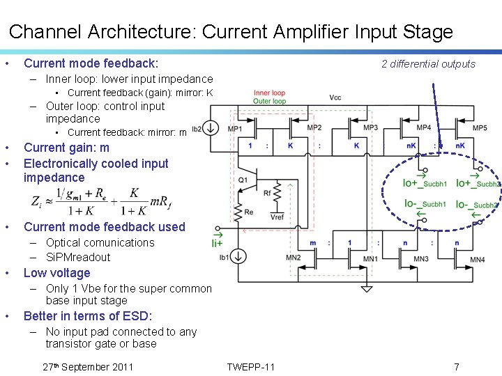
Channel Architecture: Current Amplifier Input Stage • Current mode feedback: 2 differential outputs – Inner loop: lower input impedance • Current feedback (gain): mirror: K – Outer loop: control input impedance • Current feedback: mirror: m • • Current gain: m Electronically cooled input impedance • Current mode feedback used – Optical comunications – Si. PMreadout • Low voltage – Only 1 Vbe for the super common base input stage • Better in terms of ESD: – No input pad connected to any transistor gate or base 27 th September 2011 TWEPP-11 7

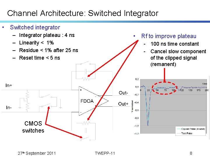
Channel Architecture: Switched Integrator • Switched integrator – – Integrator plateau : 4 ns Linearity < 1% Residue < 1% after 25 ns Reset time < 5 ns • Rf to improve plateau - 100 ns time constant - Cancel slow component of the clipped signal (remanent) CMOS switches 27 th September 2011 TWEPP-11 8

Channel Architecture: Track-And-Hold • Track-And-Hold: - 12 bit: flip-around architecture 27 th September 2011 TWEPP-11 9

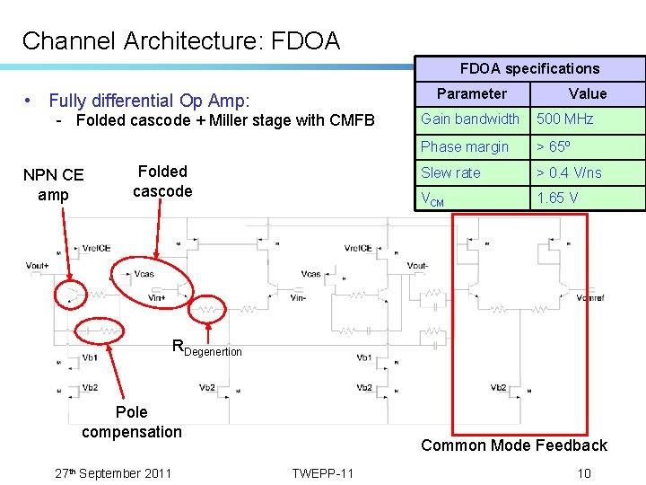
Channel Architecture: FDOA specifications Parameter • Fully differential Op Amp: - Folded cascode + Miller stage with CMFB NPN CE amp Folded cascode Value Gain bandwidth 500 MHz Phase margin > 65º Slew rate > 0. 4 V/ns VCM 1. 65 V RDegenertion Pole compensation 27 th September 2011 Common Mode Feedback TWEPP-11 10

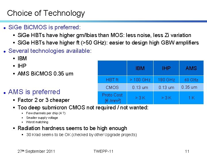
Choice of Technology Si. Ge Bi. CMOS is preferred: § Si. Ge HBTs have higher gm/Ibias than MOS: less noise, less Zi variation § Si. Ge HBTs have higher ft (>50 GHz): easier to design high GBW amplifiers Several technologies available: § IBM § IHP § AMS Bi. CMOS 0. 35 um AMS is preferred IBM IHP AMS HBT ft > 100 GHz 190 GHz 60 GHz CMOS 0. 13 um 0. 35 um Proto Cost [€ /mm 2] >3 K § Factor 2 or 3 cheaper § Too deep submicron CMOS not required / not wanted: § § § 1 K Few channels per chip (4 ? ) Smaller supply voltage Worst matching § Radiation hardness seems to be high enough § 30 Krad seems to be OK (checked by other Upgrade projects) 27 th September 2011 TWEPP-11 11

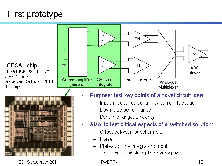
First prototype ICECAL chip: Si. Ge Bi. CMOS 0. 35 um AMS 2 mm 2 Received: October 2010 12 chips Switched integrator • Track and Hold Purpose: test key points of a novel circuit idea – Input impedance control by current feedback – Low noise performance – Dynamic range: Linearity • Also, to test critical aspects of a switched solution: – Offset between subchannels – Noise – Plateau of the integrator output • Effect of the clock jitter versus signal 27 th September 2011 TWEPP-11 12

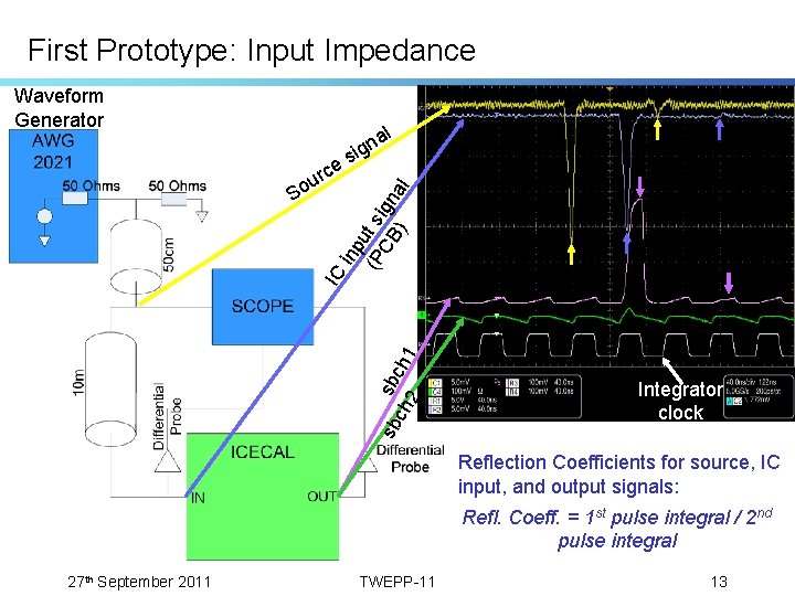
First Prototype: Input Impedance Waveform Generator e sb sbc ch 2 h 1 IC inp (P ut si CB gn al ) rc u So al n sig Integrator clock Reflection Coefficients for source, IC input, and output signals: Refl. Coeff. = 1 st pulse integral / 2 nd pulse integral 27 th September 2011 TWEPP-11 13

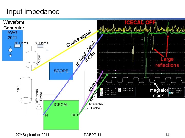
Input impedance Waveform Generator ICECAL OFF inp (P ut si CB gn al ) sb sbc ch 2 h 1 IC S rce u o al n sig 27 th September 2011 TWEPP-11 Large reflections Integrator clock 14

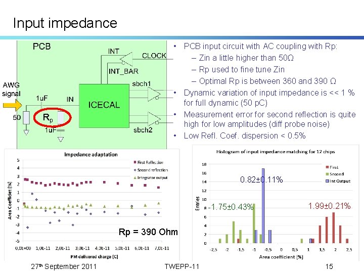
Input impedance Rp • PCB input circuit with AC coupling with Rp: – Zin a little higher than 50Ω – Rp used to fine tune Zin – Optimal Rp is between 360 and 390 Ω • Dynamic variation of input impedance is << 1 % for full dynamic (50 p. C) • Measurement error for second reflection is quite high for low amplitudes (diff probe noise) • Low Refl. Coef. dispersion < 0. 5% 0. 82± 0. 11% -1. 75± 0. 43% 1. 99± 0. 21% Rp = 390 Ohm 27 th September 2011 TWEPP-11 15

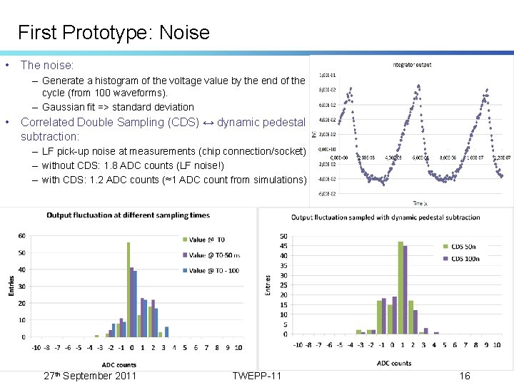
First Prototype: Noise • The noise: – Generate a histogram of the voltage value by the end of the cycle (from 100 waveforms). – Gaussian fit => standard deviation • Correlated Double Sampling (CDS) ↔ dynamic pedestal subtraction: – LF pick-up noise at measurements (chip connection/socket) – without CDS: 1. 8 ADC counts (LF noise!) – with CDS: 1. 2 ADC counts (≈1 ADC count from simulations) 27 th September 2011 TWEPP-11 16

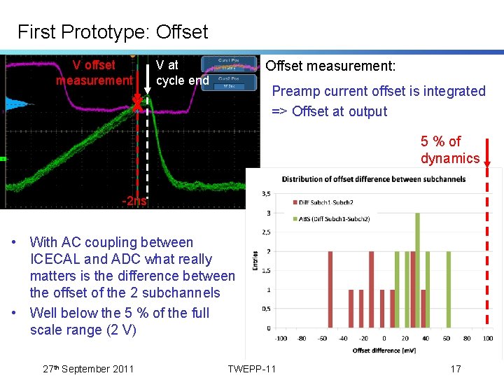
First Prototype: Offset V offset measurement V at cycle end Offset measurement: Preamp current offset is integrated => Offset at output 5 % of dynamics -2 ns • With AC coupling between ICECAL and ADC what really matters is the difference between the offset of the 2 subchannels • Well below the 5 % of the full scale range (2 V) 27 th September 2011 TWEPP-11 17

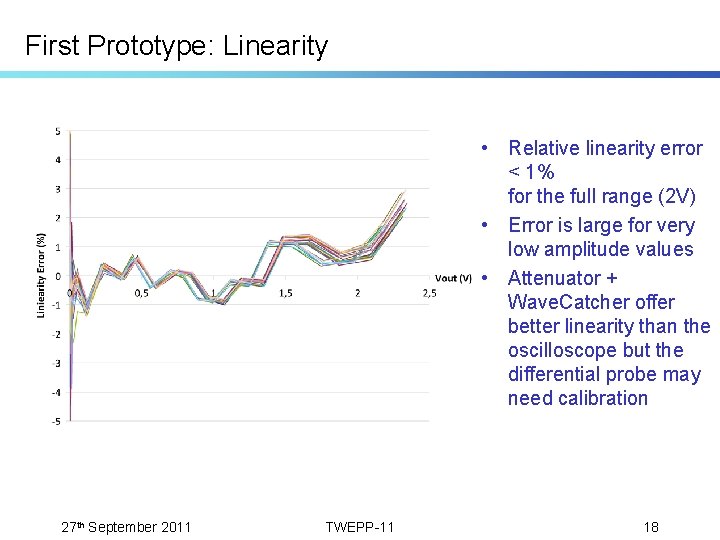
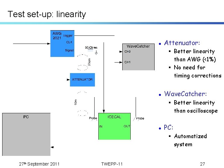
First Prototype: Linearity • Relative linearity error < 1% for the full range (2 V) • Error is large for very low amplitude values • Attenuator + Wave. Catcher offer better linearity than the oscilloscope but the differential probe may need calibration 27 th September 2011 TWEPP-11 18

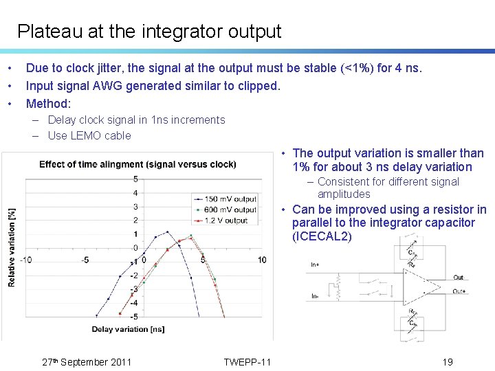
Plateau at the integrator output • • • Due to clock jitter, the signal at the output must be stable (<1%) for 4 ns. Input signal AWG generated similar to clipped. Method: – Delay clock signal in 1 ns increments – Use LEMO cable • The output variation is smaller than 1% for about 3 ns delay variation – Consistent for different signal amplitudes • Can be improved using a resistor in parallel to the integrator capacitor (ICECAL 2) 27 th September 2011 TWEPP-11 19

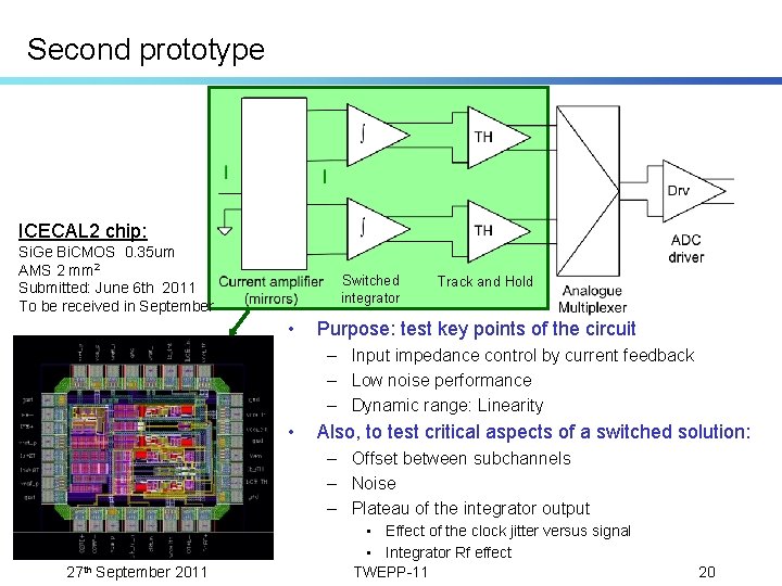
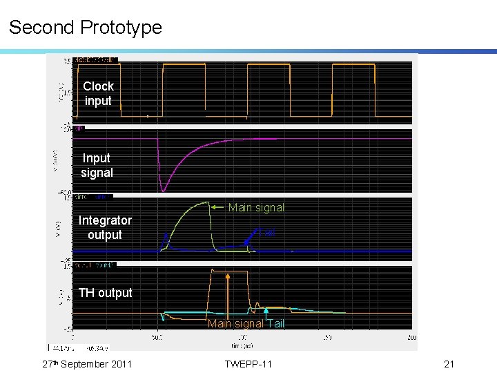
Second prototype ICECAL 2 chip: Si. Ge Bi. CMOS 0. 35 um AMS 2 mm 2 Submitted: June 6 th 2011 To be received in September Switched integrator • Track and Hold Purpose: test key points of the circuit – Input impedance control by current feedback – Low noise performance – Dynamic range: Linearity • Also, to test critical aspects of a switched solution: – Offset between subchannels – Noise – Plateau of the integrator output 27 th September 2011 • Effect of the clock jitter versus signal • Integrator Rf effect TWEPP-11 20

Second Prototype Clock input Input signal Integrator output Main signal Tail TH output Main signal Tail 27 th September 2011 TWEPP-11 21

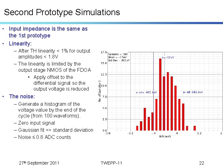
Second Prototype Simulations • Input impedance is the same as the 1 st prototype • Linearity: – After TH linearity < 1% for output amplitudes < 1. 8 V – The linearity is limited by the output stage NMOS of the FDOA • Apply offset to the differential signal so the output voltage is reduced • The noise: – Generate a histogram of the voltage value by the end of the cycle (from 100 waveforms). – Zero input signal – Gaussian fit => standard deviation – Noise ≲ 0. 8 ADC counts 27 th September 2011 TWEPP-11 22

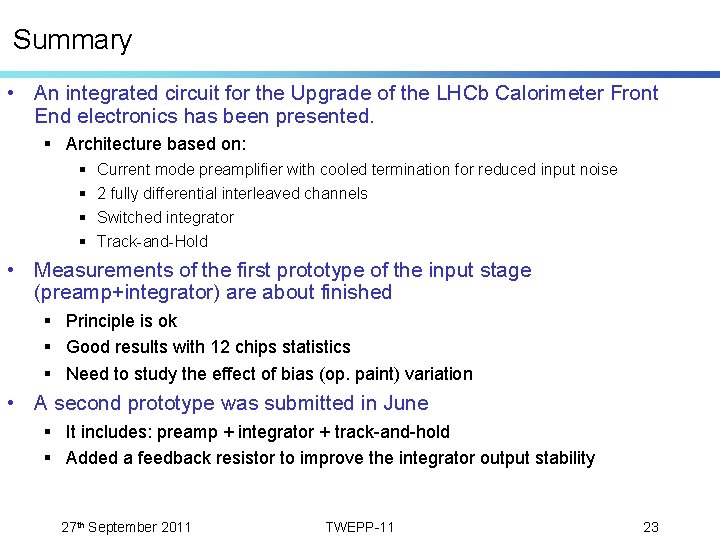
Summary • An integrated circuit for the Upgrade of the LHCb Calorimeter Front End electronics has been presented. § Architecture based on: § § Current mode preamplifier with cooled termination for reduced input noise 2 fully differential interleaved channels Switched integrator Track-and-Hold • Measurements of the first prototype of the input stage (preamp+integrator) are about finished § Principle is ok § Good results with 12 chips statistics § Need to study the effect of bias (op. paint) variation • A second prototype was submitted in June § It includes: preamp + integrator + track-and-hold § Added a feedback resistor to improve the integrator output stability 27 th September 2011 TWEPP-11 23

Back-up: 27 th September 2011 TWEPP-11 24

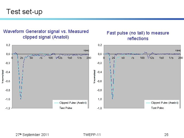
Test set-up Waveform Generator signal vs. Measured clipped signal (Anatoli) 27 th September 2011 TWEPP-11 Fast pulse (no tail) to measure reflections 25

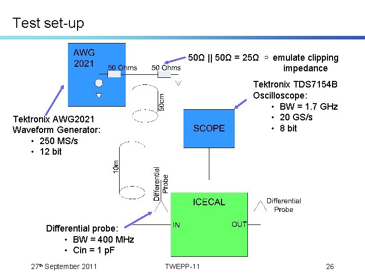
Test set-up 50Ω || 50Ω = 25Ω ⇨ emulate clipping impedance Tektronix TDS 7154 B Oscilloscope: • BW = 1. 7 GHz • 20 GS/s • 8 bit Tektronix AWG 2021 Waveform Generator: • 250 MS/s • 12 bit Differential probe: • BW = 400 MHz • Cin = 1 p. F 27 th September 2011 TWEPP-11 26

Test set-up: linearity Attenuator: § Better linearity than AWG (<1%) § No need for timing corrections Wave. Catcher: § Better linearity than oscilloscope PC: § Automatized system 27 th September 2011 TWEPP-11 27

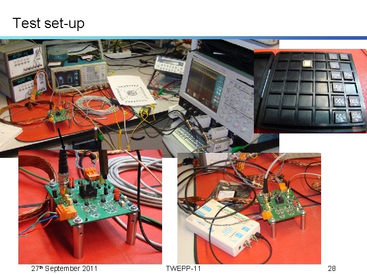
Test set-up 27 th September 2011 TWEPP-11 28