MSP 430 Teaching Materials Week 7 LowPower Modes


: § 6 operating modes; § Configured by")


: • Example: Typical current consumption (41 x")

![Low power modes (LPM): Mode Current SR bits configuration Clock signals Oscillator [ A]](https://slidetodoc.com/presentation_image/28a6c41bda4f97e5db3816716b2c3a5c/image-8.jpg "Low power modes (LPM): Mode Current SR bits configuration Clock signals Oscillator [ A]")
 characteristics: § LPM 0 to")

 selection: q Through four bits in status register (SR) in")

 q Program flow steps: § Enter Low-power mode: •")

 q Program flow steps: § An enabled interrupt event")
 q Examples of applications development using the MSP 430")


 ports, P")


 q Independent of the I/O port type (non-interruptible or interruptible), the operation")
 § Input Registers (Px. IN): • When pins are configured as GPIO,")
 § Output Registers (Px. OUT): • Each bit of these registers reflects")
 § Function Select Registers: (Px. SEL) and (Px. SEL 2): • Some")
 (1/2) q Each pin of ports P")
 § (2/2) Interrupt Edge Select Registers (Px.")


- Slides: 49
MSP 430 Teaching Materials Week 7 Low-Power Modes Hacettepe University Copyright 2009 Texas Instruments All Rights Reserved
Low-Power Modes q One of the main features of the MSP 430 families: § Low power consumption § Important in battery operated embedded systems. q Low power consumption is only accomplished: § Using low power operating modes design; § Depends on several factors such as: • Clock frequency; • Ambient temperature; • Supply voltage; • Peripheral selection; • Input/output usage; • Memory type; • . . . Copyright 2009 Texas Instruments All Rights Reserved 2
Low-Power Modes q Low power modes (LPM): § 6 operating modes; § Configured by the SR bits: CPUOFF, OSCOFF, SCG 1, SCG 0. § Active mode (AM) - highest power consumption: q Active mode: § MSP 430 starts up in this mode, which must be used when the CPU is required, i. e. , to run code § An interrupt automatically switches MSP 430 to active § Current can be reduced by running at lowest supply voltage consistent with the frequency of MCLK, e. g. VCC to 1. 8 V for f. DCO = 1 MHz • Configured by disabling the SR bits described above; • CPU is active; • All enabled clocks are active; • Current consumption: 250 A. Copyright 2009 Texas Instruments All Rights Reserved 3
Low-Power Modes § Software selection up to 5 LPM of operation; § Operation: • An interrupt event can wake up the CPU from any LPM; • Service the interrupt request; • Restore back to the LPM. Copyright 2009 Texas Instruments All Rights Reserved 4
Low-Power Modes
Low-Power Modes • Low power modes (LPM): • Example: Typical current consumption (41 x family).
Low-Power Modes
Low power modes (LPM): Mode Current SR bits configuration Clock signals Oscillator [ A] CPUOFF OSCOFF SCG 1 SCG 0 ACLK SMCLK DCO DC gen. Low-power mode 0 (LPM 0) 35 1 0 0 0 1 1 Low-power mode 1 (LPM 1) 44 1 0 0 1 1 1 0 1 1* Low-power mode 2 (LPM 2) 19 1 0 1 0 0 0 1 Low-power mode 3 (LPM 3) 0. 8 1 0 1 1 1 0 0 Low-power mode 4 (LPM 4) 0. 1 1 1 0 0 0 *DCO’s DC generator is enabled if it is used by peripherals. Copyright 2009 Texas Instruments All Rights Reserved 8
Low power operating modes q Low power modes (LPM) characteristics: § LPM 0 to LPM 3: Periodic processing based on a timer interrupt; • LPM 0: CPU and MCLK are disabled, SMCLK and ACLK remain active. Both DCO source signal and DCO’s DC generator are active. This is used when the CPU is not required but some modules require a fast clock from SMCLK and the DCO • LPM 1: Main difference to LPM 0 is the condition of enable/disable the DCO’s DC generator; • LPM 2: DCO’s DC generator is active and DCO is disabled; • LPM 3: CPU, MCLK, SMCLK, and DCO are disabled; only ACLK remains active (< 2 μA). This is the standard low-power mode when the device must wake itself at regular intervals and therefore needs a (slow) clock. It is also required if the MSP 430 must maintain a real-time clock. Copyright 2009 Texas Instruments All Rights Reserved 9
Low power operating modes § LPM 4: • The device can be wakened only by an external signal. • No clocks are active and available for peripherals. • Reduced current consumption (0. 1 μA). Copyright 2009 Texas Instruments All Rights Reserved 10
Low power modes (LPM) selection: q Through four bits in status register (SR) in CPU § SCG 0 (System clock generator 0): when set, turns off DCO, if DCOCLK is not used for MCLK or SMCLK § SCG 1 (System clock generator 1): when set, turns off the SMCLK § OSCOFF (Oscillator off): when set, turns off LFXT 1 crystal oscillator, when LFXT 1 CLK is not use for MCLK or SMCLK § CPUOFF (CPU off): when set, turns off the CPU § All are clear in active mode Copyright 2009 Texas Instruments All Rights Reserved 12
How to put in LPM q bis. w #LPM 3 , SR ; enter LPM 3 but can we wake again? q bis. w #GIE|LPM 3 , SR ; enter LPM 3 with interrupts enabled q This cannot be done in standard C, of course, and an intrinsic function is required. The function that follows is taken from intrinsics. h and sets both the low-power and GIE bits: q _low_power_mode_3 (); // enter LPM 3 with interrupts enabled Copyright 2009 Texas Instruments All Rights Reserved 13
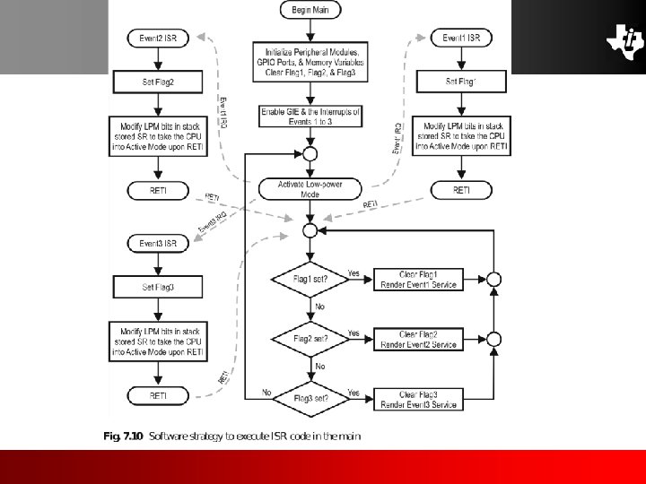
Low power operating modes (6/11) q Program flow steps: § Enter Low-power mode: • Enable/disable CPUOFF, OSCOFF, SCG 0, SCG 1 bits in SR; • LPM is now active after writing to SR! • CPU will suspend the program execution; • Disabled peripherals: – Peripherals operating with any disabled clock; – Individual control register settings. • All I/O port pins and RAM/registers are unchanged; • Wake up is now possible through any enabled interrupt. Copyright 2009 Texas Instruments All Rights Reserved 14
MCLK and Low-Power Mode q An interrupt is needed to awaken the MSP 430. q The processor handles an interrupt from a low-power mode in almost the same way as in active mode. The only difference is that MCLK must first be started so that the CPU can handle the interrupt; this replaces the first step when the CPU is active, which is to complete the current instruction. q MCLK is started automatically by the hardware for servicing interrupts and requires no intervention from the programmer. Remember that the status register is cleared when an interrupt is accepted, which puts the processor into active mode. q Similarly, MCLK is automatically turned off at the end of the ISR if the MSP 430 returns to a low-power mode when the status register is restored. Copyright 2009 Texas Instruments All Rights Reserved 15
Low power operating modes (7/11) q Program flow steps: § An enabled interrupt event wakes the MSP 430; § Enter ISR: • The operating mode is saved on the stack during ISR; • The PC and SR are stored on the stack; • Interrupt vector is moved to the PC; • The CPUOFF, SCG 1, and OSCOFF bits are automatically reset, enabling normal CPU operation; • § Corresponding IFG flag cleared on single source flags. Returning from the ISR: • The original SR is popped from the stack, restoring the previous operating mode; • The SR bits are restored from the stack returning to a different operating mode after RETI instruction. Copyright 2009 Texas Instruments All Rights Reserved 16
Low power operating modes (8/11) q Examples of applications development using the MSP 430 with and without low power modes consideration: Example Without low power mode With low power mode Toggling the bit 0 of port 1 (P 1. 0) periodically Endless loop (100 % CPU load) LPM 0 Timer interrupt UART to transmit the received message at a 9600 baud rate Polling UART receive (100 % CPU load) UART receive interrupt (0. 1 % CPU load) Set/reset during a time interval, periodically, of the peripheral connected to the bit 2 of port 1 (P 1. 2) Endless loop (100 % CPU load) Setup output unit (Zero CPU load) Power manage external devices like Op-Amp Putting the OPA Quiescent (Average current: 1 A) Shutdown the Op-Amp between data acquisition (Average current: 0. 06 A) Power manage internal devices like Comparator A Always active (Average typical current: 35 A) Disable Comparator A between data acquisition Endless loop (100 % CPU load) Using LPMs while the LED is switch off: LPM 3: 1. 4 A LPM 4: 0. 3 A Configure unused ports in output direction P 1 interrupt service routine Respond to button-press interrupt in P 1. 0 and toggle LED on P 2. 1 Copyright 2009 Texas Instruments All Rights Reserved 17
// timint. C 1. c - toggles LEDs with period of about 1. 0 s // Toggle LEDs in ISR using interrupts from timer A CCR 0 // in Up mode with period of about 0. 5 s // Timer clock is SMCLK divided by 8, up mode , period 50000 // Olimex 1121 STK , LED 1 , 2 active low on P 2. 3, 4 // J H Davies , 2006 -10 -11; IAR Kickstart version 3. 41 A // ---------------------------------------------------------------------#include <io 430 x 11 x 1. h> // Specific device #include <intrinsics. h> // Intrinsic functions // ---------------------------------------------------------------------// Pins for LEDs #define LED 1 BIT 3 #define LED 2 BIT 4 // ---------------------------------------------------------------------void main (void) { { WDTCTL = WDTPW|WDTHOLD; // Stop watchdog timer P 2 OUT = ˜LED 1; // Preload LED 1 on , LED 2 off P 2 DIR = LED 1|LED 2; // Set pins with LED 1 , 2 to output TACCR 0 = 49999; // Upper limit of count for TAR TACCTL 0 = CCIE; // Enable interrupts on Compare 0 TACTL = MC_1|ID_3|TASSEL_2|TACLR; // Set up and start Timer A // "Up to CCR 0" mode , divide clock by 8, clock from SMCLK , clear timer __enable _interrupt (); // Enable interrupts (intrinsic) for (; ; ) { // Loop forever doing nothing } // Interrupts do the work __low_power_mode_0 (); // Enter LPM 0 } } // Interrupts do the work } // -----------------------------------// Interrupt service routine for Timer A channel 0 // ---------------------------------------------------------------------// Interrupt service routine for Timer A channel 0 #pragma vector = TIMERA 0_VECTOR // -----------------------------------__interrupt void TA 0_ISR (void) #pragma vector = TIMERA 0_VECTOR { __interrupt void TA 0_ISR (void) P 2 OUT ˆ= LED 1|LED 2; // Toggle LEDs { } P 2 OUT ˆ= LED 1|LED 2; // Toggle LEDs } Copyright 2009 Texas Instruments All Rights Reserved 18
Assembly version q interrupts from Timer_A. The device enters low-power mode 0 between interrupts. Inf. Loop: bis. w #LPM 0|GIE , SR ; this is added ; Enable ints and low power mode 0 jmp Inf. Loop ; Infinite loop (should never happen) Copyright 2009 Texas Instruments All Rights Reserved 19
; timrint 1. s 43 - toggles LEDs with period of about 1 s ; TACCR 0 interrupts from timer A with period of about 0. 5 s ; Timer clock is SMCLK divided by 8, up mode , period 50000 ; Olimex 1121 STK , LED 1 , 2 active low on P 2. 3, 4 ; -----------------------------------#include <msp 430 x 11 x 1. h> ; Header file for this device ; -----------------------------------; Pins for LED on port 2 LED 1 EQU BIT 3 LED 2 EQU BIT 4 ; -----------------------------------RSEG CSTACK ; Create stack (in RAM) ; -----------------------------------RSEG CODE ; Program goes in code memory Reset: ; Execution starts here mov. w #SFE(CSTACK), SP ; Initialize stack pointer main: ; Equivalent to start of main() in C mov. w #WDTPW|WDTHOLD , & WDTCTL ; Stop watchdog timer mov. b #LED 2 , & P 2 OUT ; Preload LED 1 on , LED 2 off bis. b #LED 1|LED 2 , & P 2 DIR ; Set pins with LED 1 , 2 to output mov. w #49999 , & TACCR 0 ; Period for up mode mov. w #CCIE , & TACCTL 0 ; Enable interrupts on Compare 0 mov. w #MC_1|ID_3|TASSEL_2|TACLR , & TACTL ; Set up Timer A ; Up mode , divide clock by 8, clock from SMCLK , clear TAR bis. w #GIE , SR ; Enable interrupts (just TACCR 0) jmp $ ; Loop forever; interrupts do all ; -----------------------------------; Interrupt service routine for TACCR 0 , called when TAR = TACCR 0 ; No need to acknowledge interrupt explicitly - done automatically TA 0_ISR: ; ISR for TACCR 0 CCIFG xor. b #LED 1|LED 2 , & P 2 OUT ; Toggle LEDs reti ; That's all: return from interrupt ; -----------------------------------COMMON INTVEC ; Segment for vectors (in Flash) ORG TIMERA 0_VECTOR DW TA 0_ISR ; ISR for TA 0 interrupt ORG RESET_VECTOR DW Reset ; Address to start execution END interrupts from Timer_A. The device enters low-power mode 0 Inf. Loop: bis. w #LPM 0|GIE , SR ; this is added ; Enable ints and low power mode 0 jmp Inf. Loop ; Infinite loop (should never happen) Copyright 2009 Texas Instruments All Rights Reserved 20
q We could save more power by using low-power mode 3 rather than mode 0. Two small changes are needed. The TASSEL bits in TACTL must be adjusted so that the timer runs from ACLK rather than SMCLK. Then the MCU can be put into LPM 3 instead of LPM 0 between interrupts. Copyright 2009 Texas Instruments All Rights Reserved 21
Returning from a Low-Power Mode to the Main Function q Sometimes it is not appropriate to carry out all actions in an ISR and it is better to return to the main function in active mode. To be more precise, this means returning to the function that put the device into the low-power mode. q In this case we must clear all the low-power bits in the saved value of SR on the stack before it is restored at the end of the interrupt service routine. This sounds alarming but is actually straightforward, particularly in C because an intrinsic function _ _low_power_mode_off_on_exit() is available to do the job. Copyright 2009 Texas Instruments All Rights Reserved 22
Returning from a Low-Power Mode to the Main Function Part of program to toggle LEDs using interrupts from Timer_A. The device enters low-power mode 0, is awakened by an interrupt and returns to the main function to toggle the LED. for (; ; ) { // Loop forever __low_power_mode_3 (); // Enter low power mode LPM 3 // Wait here , pace loop until timer expires and ISR restores Active Mode P 2 OUT ˆ= LED 1|LED 2; // Toggle LEDs } } // -----------------------------------// Interrupt service routine for Timer A channel 0 // Processor remains in Active Mode after ISR // -----------------------------------#pragma vector = TIMERA 0_VECTOR __interrupt void TA 0_ISR (void) { __low_power_mode_off_on_exit(); // Restore Active Mode on return } Copyright 2009 Texas Instruments All Rights Reserved 23
Returning from a Low-Power Mode to the Main Function q The main function is now like the paced loop of except that the processor goes to sleep and waits to be awakened by an interrupt from the timer instead of polling the overflow flag. In fact _ _low_ power_mode_3() behaves just like a simple delay function. The ISR is trivial and contains only one line for the intrinsic function to clear the stacked lowpower mode. q The more general function _ _bic_SR_register_on_exit() can be used to clear selected bits in SR if finer control is required. q It is also called _BIC_SR_IRQ(). Copyright 2009 Texas Instruments All Rights Reserved 24
Returning from a Low-Power Mode to the Main Function Part of program timain 1. s 43 to toggle LEDs using interrupts from Timer_A. The device enters lowpower mode 0, is awakened by an interrupt and returns to the main function to toggle the LED. Inf. Loop: bis. w #LPM 3|GIE, SR ; Enable interrupts and enter LPM 3 ; Wait here, pace loop until timer expires and ISR restores Active Mode nop ; Helps debugging xor. b #LED 1|LED 2 , & P 2 OUT ; Toggle LEDs jmp Inf. Loop ; Infinite loop ; ---------------------------------; Interrupt service routine for TACCR 0 , called when TAR = TACCR 0 ; No need to acknowledge interrupt explicitly - done automatically TA 0_ISR: ; ISR for TACCR 0 CCIFG bic. w #LPM 3 , 0(SP) ; Delete LPM 3 on exit: Active Mode reti ; That's all: return from interrupt Copyright 2009 Texas Instruments All Rights Reserved 25
Input/0 utput Interfacing q Up to ten 8 -bit digital Input/Output (I/O) ports, P 1 to P 10 (depending on the MSP 430 device); q I/O ports P 1 and P 2 have interrupt capability; q Each interrupt for these I/O lines can be individually configured: § To provide an interrupt on a rising or falling edge; § All interruptible I/O lines source a single interrupt vector. q The available digital I/O pins for the hardware development tools: § e. Z 430 -F 2013: 10 pins - Port P 1 (8 bits) and Port P 2 (2 bits); § e. Z 430 -RF 2500: 32 pins - Port P 1 to P 4 (8 bits); § Experimenter’s board: 80 pins – Port P 1 to P 10 (8 bits). Copyright 2009 Texas Instruments All Rights Reserved 26
Input/0 utput Interfacing q Each I/O port can be: § Programmed independently for each bit; § Combine input, output, and interrupt functionality; § Edge-selectable input interrupt capability for all 8 bits of ports P 1 and P 2; § Read/write access to port-control registers is supported § Individually programmable pull-up/pull-down resistor (2 xx family only). Copyright 2009 Texas Instruments All Rights Reserved 27
Input/0 utput Interfacing q The port pins can be individually configured as I/O for special functions, such as: § USART – Universal Synchronous/Asynchronous Receive/Transmit for serial data; § Input comparator for analogue signals; § Analogue-to-Digital converter; § Others functions (see specific datasheet for details). Copyright 2009 Texas Instruments All Rights Reserved 28
Registers (1/6) q Independent of the I/O port type (non-interruptible or interruptible), the operation of the ports is configured by user software, as defined by the following registers: § Direction Registers (Px. DIR): • Read/write 8 -bit registers; • Select the direction of the corresponding I/O pin, regardless of the selected function of the pin (general purpose I/O or as a special function I/O); • For other module functions, must be set as required by the other function. • Px. DIR configuration: Bit = 1: the individual port pin is set as an output; Bit = 0: the individual port pin is set as an input. Copyright 2009 Texas Instruments All Rights Reserved 29
Registers (2/6) § Input Registers (Px. IN): • When pins are configured as GPIO, each bit of these read-only registers reflects the input signal at the corresponding I/O pin; • Px. IN configuration: Bit = 1: The input is high; Bit = 0: The input is low; • Tip: Avoid writing to these read-only registers because it will result in increased current consumption. Copyright 2009 Texas Instruments All Rights Reserved 30
Registers (3/6) § Output Registers (Px. OUT): • Each bit of these registers reflects the value written to the corresponding output pin. • Px. OUT configuration: Bit = 1: The output is high; Bit = 0: The output is low. – Note: the Px. OUT Register is read-write. This means that the previous value written to it can be read back and modified to generate the next output signal. Copyright 2009 Texas Instruments All Rights Reserved 31
Registers (5/6) § Function Select Registers: (Px. SEL) and (Px. SEL 2): • Some port pins are multiplexed with other peripheral module functions (see the device-specific datasheet); • These bits: Px. SEL and Px. SEL 2 (see specific device datasheet), are used to select the pin function: • – I/O general purpose port; – Peripheral module function. Px. SEL configuration: Bit = 0: I/O Function is selected for the pin; Bit = 1: Peripheral module function enabled for pin. Copyright 2009 Texas Instruments All Rights Reserved 32
Interruptible ports (P 1 and P 2) (1/2) q Each pin of ports P 1 and P 2 is able to make an interrupt request; q Pins are configured with additional registers: § Interrupt Enable (Px. IE): • Read-write register to enable interrupts on individual pins; • Px. IE configuration: Bit = 1: The interrupt is enabled; Bit = 0: The interrupt is disabled. • Each Px. IE bit enables the interrupt request associated with the corresponding Px. IFG interrupt flag; • Writing to Px. OUT and/or Px. DIR can result in setting Px. IFG. Copyright 2009 Texas Instruments All Rights Reserved 33
Interruptible ports (P 1 and P 2) § (2/2) Interrupt Edge Select Registers (Px. IES): • Selects the transition on which an interrupt occurs (if Px. IE and GIE are set); • Px. IES configuration: Bit = 1: Interrupt flag is set on a high-to-low transition; Bit = 0: Interrupt flag is set on a low-to-high transition. § Interrupt Flag Registers (Px. IFG) • Set automatically when a programmed signal transition (edge) occurs; • Px. IFG flag can be set and must be reset by software. • Px. IFG configuration: Bit = 0: No interrupt is pending; Bit = 1: An interrupt is pending. Copyright 2009 Texas Instruments All Rights Reserved 34
Interrupts on Digital Inputs q Ports P 1 and P 2 can request an interrupt when the value on an input changes. This is one of the few interrupts that remains active in LPM 4 and is therefore useful to wake the CPU in portable equipment that lies idle for a long time q Interrupts for port P 1 are controlled by the registers P 1 IE and P 1 IES, and similarly for port P 2. There is a single vector for each port, so the user must check P 1 IFG to determine the bit that caused the interrupt. This bit must be cleared explicitly; it does not happen automatically as with interrupts that have a single source. q The direction of the transition that causes the interrupt can be changed in P 1 IES at any time by the program. This is useful if both edges of a pulse need to be detected, for example, when a button is pressed and released. There is a danger that spurious interrupts may be generated, so it is a good idea to disable this interrupt, change P 1 IES, and clear any spurious flags in P 1 IFG before reenabling the interrupt! Copyright 2009 Texas Instruments All Rights Reserved 35
// butled 4. c - press button B 1 to light LED 1 // Responds to interrupts on input pin , LPM 4 between interrupts // Olimex 1121 STK board , LED 1 active low on P 2. 3, // button B 1 active low on P 2. 1 // J H Davies , 2006 -11 -18; IAR Kickstart version 3. 41 A // -----------------------------------#include <io 430 x 11 x 1. h> // Specific device #include <intrinsics. h> // Intrinsic functions // -----------------------------------void main (void) { WDTCTL = WDTPW | WDTHOLD; // Stop watchdog timer P 2 OUT_bit. P 2 OUT_3 = 1; // Preload LED 1 off (active low!) P 2 DIR_bit. P 2 DIR_3 = 1; // Set pin with LED 1 to output P 2 IE_bit. P 2 IE_1 = 1; // Enable interrupts on edge P 2 IES_bit. P 2 IES_1 = 1; // Sensitive to negative edge (H->L) do { P 2 IFG = 0; // Clear any pending interrupts. . . } while (P 2 IFG != 0); //. . . until none remain for (; ; ) { // Loop forever (should not need) __low_power_mode_4 (); // LPM 4 with int'pts , all clocks off } // (RAM retention mode) } // -----------------------------------Copyright 2009 Texas Instruments All Rights Reserved 36
// Interrupt service routine for port 2 inputs // Only one bit is active so no need to check which // Toggle LED , toggle edge sensitivity , clear any pending interrupts // Device returns to low power mode automatically after ISR // ---------------------------------#pragma vector = PORT 2_VECTOR __interrupt void PORT 2_ISR (void) { P 2 OUT_bit. P 2 OUT_3 ˆ= 1; // Toggle LED P 2 IES_bit. P 2 IES_3 ˆ= 1; // Toggle edge sensitivity do { P 2 IFG = 0; // Clear any pending interrupts. . . } while (P 2 IFG != 0); //. . . until none remain } Copyright 2009 Texas Instruments All Rights Reserved 37
Multiplexed Inputs: Scanning a Matrix Keypad q Many products require numerical input and provide a keypad for the user. These often have 12 keys, like a telephone, or more. An individual connection for each switch would use an exorbitant number of pins so they are usually arranged as a matrix instead. Only seven pins are needed for a 12 -key pad, or eight pins for 16 keys. q As usual this economy comes at a price. The matrix must be scanned, which is more complicated than reading individual inputs. Moreover, the reading may become ambiguous if more than one key is depressed Copyright 2009 Texas Instruments All Rights Reserved 38
q There are, as usual, many ways of dealing with a keypad. Here is a straightforward approach, although it needs refinement in practice. Do not worry about debouncing at this stage and assume that no more than one switch is closed. Connect the rows Y 1–Y 4 as inputs to the microcontroller while the columns X 1–X 3 are driven by outputs. (It could equally well be the other way around. ) Pull-up resistors are required on the inputs. These could be internal for the MSP 430 F 2 xx family but must be provided externally for other devices Copyright 2009 Texas Instruments All Rights Reserved 39
1. Drive X 1 low and the other columns X 2 and X 3 high. This makes the switches in column X 1 active and the corresponding Y input goes low if a button is pressed. Thus we can detect the state of switches 1, 4, 7, or *. The switches in the other columns have no effect because both of their terminals are at VCC. 2. Drive X 2 low and the other columns high to read the switches in column X 2. 3. Repeat this for column X 3. 4. This process can be repeated as often as required Copyright 2009 Texas Instruments All Rights Reserved 40
q A problem with this simple method arises if two buttons, such as 1 and 2, are pressed, which short-circuits the column drives X 1 and X 2. This damages the output of the microcontroller if they are connected directly. Resistors should therefore be connected between the pins of the microcontroller and the columns of the keypad. Copyright 2009 Texas Instruments All Rights Reserved 41
q It is a waste of energy to scan the keypad when no button is being pressed. In this case it is more efficient to drive all columns low and wait for an interrupt generated by a falling edge on any of the row inputs. q The keypad can then be scanned to determine which key has been pressed. Copyright 2009 Texas Instruments All Rights Reserved 42
q Often in applications with keypads, the condition can occur where a key can be held or stuck down, causing excess current consumption and reducing the battery life of a battery-operated product. q This application report shows a solution. The keypad interface in this report, based on the MSP 430, draws. 1 u. A while waiting for a key press, is completely interrupt driven requring no polling, and consumes a maximum of only 2 u. A at 3 V if all keys are pressed and held simutaneously. q See Implementing an Ultralow-Power Keypad Interface with the MSP 430 http: //www. ti. com/lit/an/slaa 139. pdf Copyright 2009 Texas Instruments All Rights Reserved 43
Implementing an Ultralow-Power Keypad Interface • 100 n. A typical current consumption while waiting for key press • 2 µA maximum current consumption if all keys are held simultaneously • No polling required • No crystal required • Minimum external components • Suitable for any MSP 430 device Copyright 2009 Texas Instruments All Rights Reserved 44
Copyright 2009 Texas Instruments All Rights Reserved 45
Implementing an Ultralow-Power Keypad Interface q The rows of the keypad are connected to port pins P 3. 0 – P 3. 3. The columns are connected to pins P 1. 0 – P 1. 2. Connecting the rows to port 3 pins, instead of port 1 pins, leaves the other port 1 pins for other interrupt sources, because the P 1 pins have interrupt capability, but the P 3 pins do not. q In normal mode, while the circuit is awaiting a key press (wait-for-press mode), the rows are driven high (1), and the P 1. x column pins are configured as inputs, with interrupts enabled and set to interrupt on a rising edge. The 4. 7 MΩ pulldown resistors hold the inputs low in this state. The MSP 430 is then put into low-power mode 4, where the MSP 430 current consumption is about 100 n. A. This state is maintained indefinitely until a key is pressed. The circuit is completely interrupt-driven with no need for polling. Copyright 2009 Texas Instruments All Rights Reserved 46
q After a key has been pressed, the MSP 430 goes into a wait-for-release mode in which it drives high only the necessary row for the key being pressed (other rows are driven low). q It reconfigures the P 1. x I/O lines to interrupt on a falling edge, and it goes back into low power mode 4, waiting for the release of the key. Again, there is no polling necessary at this point. The detection of the key release is completely interrupt driven allowing the microcontroller to stay asleep while the key is held, thus reducing current consumption. q Once the key is released, the debounce delay is again executed. After the debounce delay, the keypad is scanned again to determine if any other keys are being held. If so, the wait-for-release mode continues, waiting for all keys to be released. When all keys are released the MSP 430 goes back to the wait-for-press mode again. Copyright 2009 Texas Instruments All Rights Reserved 47
q During the wait-for-release mode, only one row of the keypad is driven high, therefore limiting the maximum amount of current consumption to the condition where all three keys on a single row are pressed and held. For a 3 -V system, that equates to about 2 µA. Any other key press does not result in increased current consumption because the corresponding row is not driven high. q In this 3× 4 keypad example, the rows are driven rather than the columns to limit the maximum current consumption by the circuit when all keys are pressed and held simultaneously. Had the columns been driven instead, the rows would have had the pulldown resistors, therefore increasing the number of paths to ground when all the keys are held and increasing the possible current consumption. Copyright 2009 Texas Instruments All Rights Reserved 48
Copyright 2009 Texas Instruments All Rights Reserved 49