JEM FDR Design and Implementation JEP system requirements
- Slides: 37

JEM FDR: Design and Implementation JEP system requirements Architecture Modularity Data Formats Data Flow Challenges : Latency Connectivity, high-speed data paths JEM revisions JEM 1. 1 - implementation details Daughter modules Energy sum algorithms FPGA resource use Performance Production tests 5 th April, 2005 JEM FDR 1

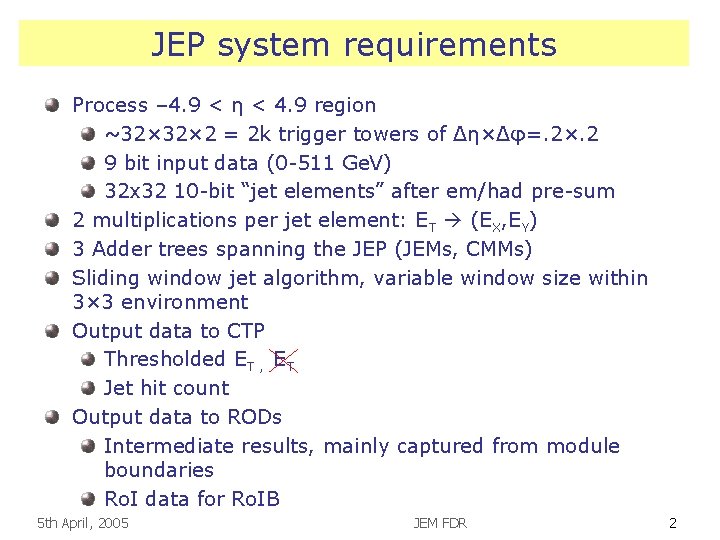
JEP system requirements Process – 4. 9 < η < 4. 9 region ~32× 2 = 2 k trigger towers of Δη×Δφ=. 2×. 2 9 bit input data (0 -511 Ge. V) 32 x 32 10 -bit “jet elements” after em/had pre-sum 2 multiplications per jet element: ET (EX, EY) 3 Adder trees spanning the JEP (JEMs, CMMs) Sliding window jet algorithm, variable window size within 3× 3 environment Output data to CTP Thresholded ET , ET Jet hit count Output data to RODs Intermediate results, mainly captured from module boundaries Ro. I data for Ro. IB 5 th April, 2005 JEM FDR 2

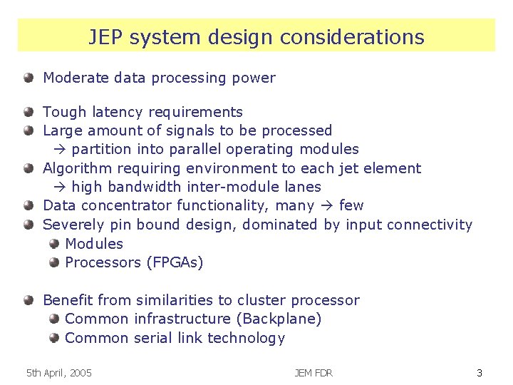
JEP system design considerations Moderate data processing power Tough latency requirements Large amount of signals to be processed partition into parallel operating modules Algorithm requiring environment to each jet element high bandwidth inter-module lanes Data concentrator functionality, many few Severely pin bound design, dominated by input connectivity Modules Processors (FPGAs) Benefit from similarities to cluster processor Common infrastructure (Backplane) Common serial link technology 5 th April, 2005 JEM FDR 3

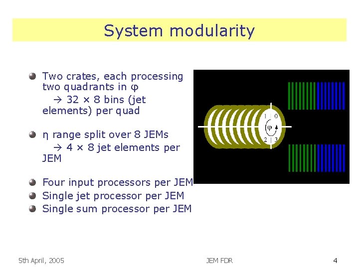
System modularity Two crates, each processing two quadrants in φ 32 × 8 bins (jet elements) per quad η range split over 8 JEMs 4 × 8 jet elements per JEM Four input processors per JEM Single jet processor per JEM Single sum processor per JEM 5 th April, 2005 JEM FDR 4

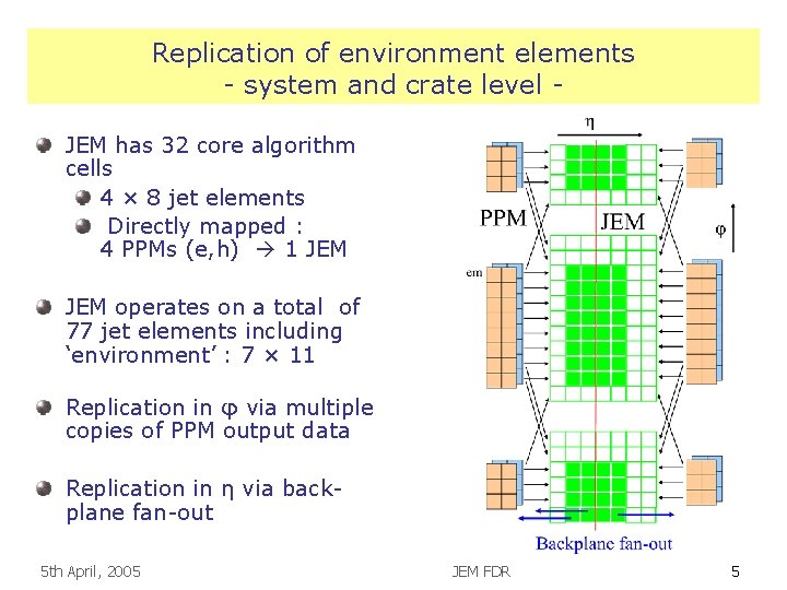
Replication of environment elements - system and crate level JEM has 32 core algorithm cells 4 × 8 jet elements Directly mapped : 4 PPMs (e, h) 1 JEM operates on a total of 77 jet elements including ‘environment’ : 7 × 11 Replication in φ via multiple copies of PPM output data Replication in η via backplane fan-out 5 th April, 2005 JEM FDR 5

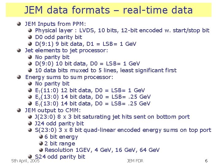
JEM data formats – real-time data JEM Inputs from PPM: Physical layer : LVDS, 10 bits, 12 -bit encoded w. start/stop bit D 0 odd parity bit D(9: 1) 9 bit data, D 1 = LSB= 1 Ge. V Jet elements to jet processor: No parity bit D(9: 0) 10 bit data, D 0 = LSB= 1 Ge. V 10 data bits muxed to 5 lines, least significant first Energy sums to sum processor: No parity bit ET(11: 0) 12 bit data, D 0 = LSB= 1 Ge. V EX(13: 0) 14 bit data, D 0 = LSB=. 25 Ge. V EY(13: 0) 14 bit data, D 0 = LSB=. 25 Ge. V JEM output to CMM: J(23: 0) 8 x 3 bit saturating jet hits sent on bottom port J 24 odd parity bit S(23: 0) 3 x 8 bit quad-linear encoded energy sums on top port 6 bit energy 2 bit range Resolution 1 GEV, 4 Ge. V, 16 Ge. V, 64 Ge. V S 24 odd parity bit 5 th April, 2005 JEM FDR 6

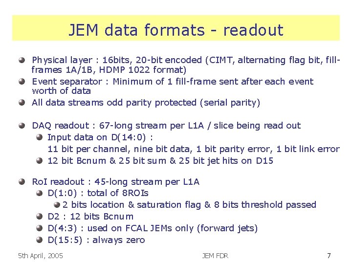
JEM data formats - readout Physical layer : 16 bits, 20 -bit encoded (CIMT, alternating flag bit, fillframes 1 A/1 B, HDMP 1022 format) Event separator : Minimum of 1 fill-frame sent after each event worth of data All data streams odd parity protected (serial parity) DAQ readout : 67 -long stream per L 1 A / slice being read out Input data on D(14: 0) : 11 bit per channel, nine bit data, 1 bit parity error, 1 bit link error 12 bit Bcnum & 25 bit sum & 25 bit jet hits on D 15 Ro. I readout : 45 -long stream per L 1 A D(1: 0) : total of 8 ROIs 2 bits location & saturation flag & 8 bits threshold passed D 2 : 12 bits Bcnum D(4: 3) : used on FCAL JEMs only (forward jets) D(15: 5) : always zero 5 th April, 2005 JEM FDR 7

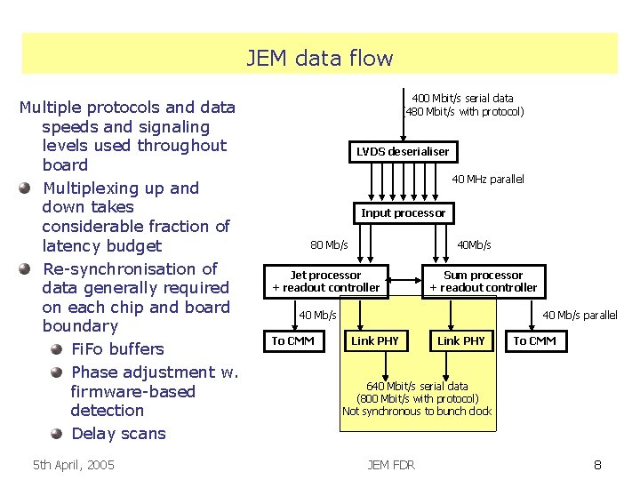
JEM data flow Multiple protocols and data speeds and signaling levels used throughout board Multiplexing up and down takes considerable fraction of latency budget Re-synchronisation of data generally required on each chip and board boundary Fi. Fo buffers Phase adjustment w. firmware-based detection Delay scans 5 th April, 2005 400 Mbit/s serial data (480 Mbit/s with protocol) LVDS deserialiser 40 MHz parallel Input processor 80 Mb/s 40 Mb/s Jet processor + readout controller Sum processor + readout controller 40 Mb/s To CMM 40 Mb/s parallel Link PHY To CMM 640 Mbit/s serial data (800 Mbit/s with protocol) Not synchronous to bunch clock JEM FDR 8

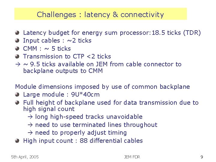
Challenges : latency & connectivity Latency budget for energy sum processor: 18. 5 ticks (TDR) Input cables : ~2 ticks CMM : ~ 5 ticks Transmission to CTP <2 ticks ~ 9. 5 ticks available on JEM from cable connector to backplane outputs to CMM Module dimensions imposed by use of common backplane Large module : 9 U*40 cm Full height of backplane used for data transmission due to high signal count long high-speed tracks unavoidable need to use terminated lines throughout need to properly adjust timing High input count : 88 differential cables 5 th April, 2005 JEM FDR 9

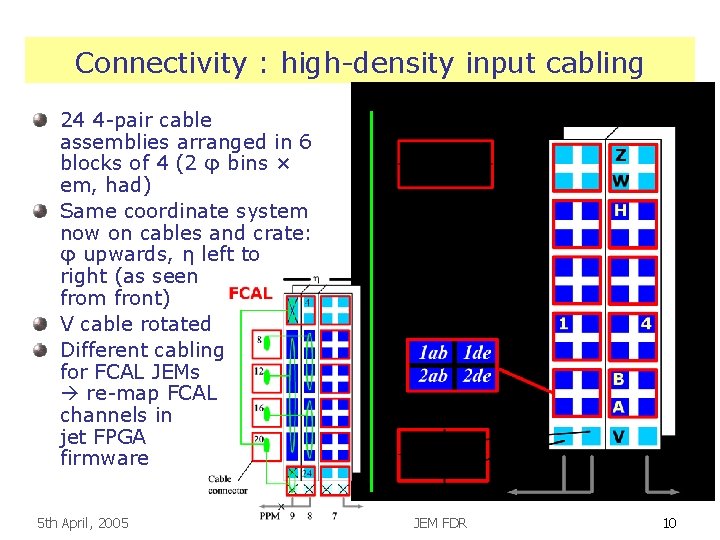
Connectivity : high-density input cabling 24 4 -pair cable assemblies arranged in 6 blocks of 4 (2 φ bins × em, had) Same coordinate system now on cables and crate: φ upwards, η left to right (as seen from front) V cable rotated Different cabling for FCAL JEMs re-map FCAL channels in jet FPGA firmware 5 th April, 2005 JEM FDR 10

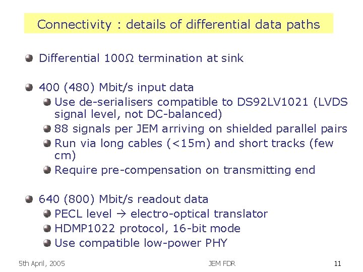
Connectivity : details of differential data paths Differential 100Ω termination at sink 400 (480) Mbit/s input data Use de-serialisers compatible to DS 92 LV 1021 (LVDS signal level, not DC-balanced) 88 signals per JEM arriving on shielded parallel pairs Run via long cables (<15 m) and short tracks (few cm) Require pre-compensation on transmitting end 640 (800) Mbit/s readout data PECL level electro-optical translator HDMP 1022 protocol, 16 -bit mode Use compatible low-power PHY 5 th April, 2005 JEM FDR 11

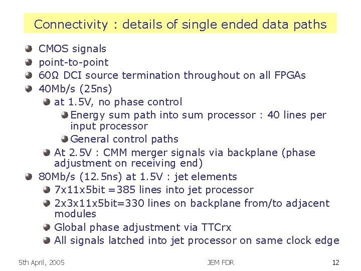
Connectivity : details of single ended data paths CMOS signals point-to-point 60Ω DCI source termination throughout on all FPGAs 40 Mb/s (25 ns) at 1. 5 V, no phase control Energy sum path into sum processor : 40 lines per input processor General control paths At 2. 5 V : CMM merger signals via backplane (phase adjustment on receiving end) 80 Mb/s (12. 5 ns) at 1. 5 V : jet elements 7 x 11 x 5 bit =385 lines into jet processor 2 x 3 x 11 x 5 bit=330 lines on backplane from/to adjacent modules Global phase adjustment via TTCrx All signals latched into jet processor on same clock edge 5 th April, 2005 JEM FDR 12

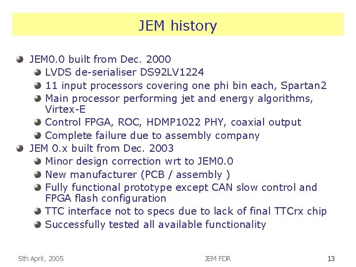
JEM history JEM 0. 0 built from Dec. 2000 LVDS de-serialiser DS 92 LV 1224 11 input processors covering one phi bin each, Spartan 2 Main processor performing jet and energy algorithms, Virtex-E Control FPGA, ROC, HDMP 1022 PHY, coaxial output Complete failure due to assembly company JEM 0. x built from Dec. 2003 Minor design correction wrt to JEM 0. 0 New manufacturer (PCB / assembly ) Fully functional prototype except CAN slow control and FPGA flash configuration TTC interface not to specs due to lack of final TTCrx chip Successfully tested all available functionality 5 th April, 2005 JEM FDR 13

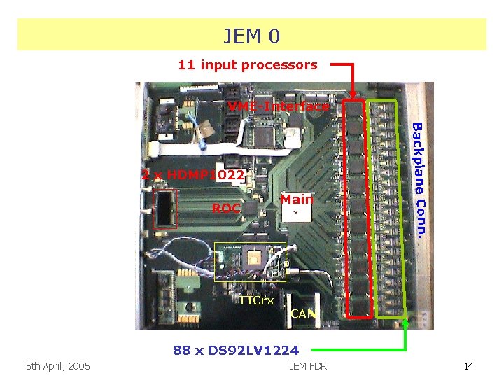
JEM 0 11 input processors VME-Interface ROC TTCrx Main Backplane Conn. 2 x HDMP 1022 CAN 88 x DS 92 LV 1224 5 th April, 2005 JEM FDR 14

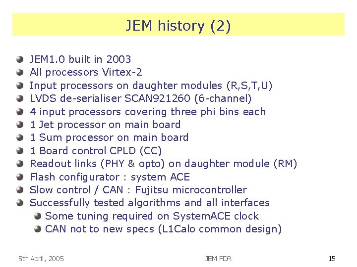
JEM history (2) JEM 1. 0 built in 2003 All processors Virtex-2 Input processors on daughter modules (R, S, T, U) LVDS de-serialiser SCAN 921260 (6 -channel) 4 input processors covering three phi bins each 1 Jet processor on main board 1 Sum processor on main board 1 Board control CPLD (CC) Readout links (PHY & opto) on daughter module (RM) Flash configurator : system ACE Slow control / CAN : Fujitsu microcontroller Successfully tested algorithms and all interfaces Some tuning required on System. ACE clock CAN not to new specs (L 1 Calo common design) 5 th April, 2005 JEM FDR 15

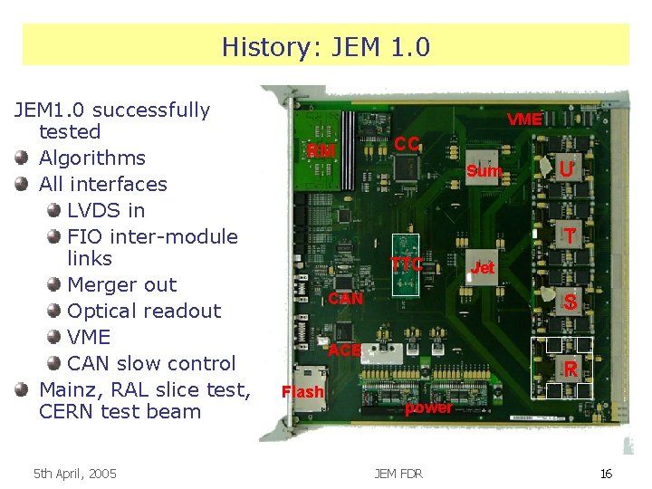
History: JEM 1. 0 successfully tested Algorithms All interfaces LVDS in FIO inter-module links Merger out Optical readout VME CAN slow control Mainz, RAL slice test, CERN test beam 5 th April, 2005 VME RM CC Sum U T TTC CAN S ACE Flash Jet R power JEM FDR 16

JEM 1. 1 in production now Identical to JEM 1. 0 Additional daughter module: Control Module (CM) CAN VME control Fan-out of configuration lines Expected back from assembly soooon 5 th April, 2005 JEM FDR 17

JEM details –main board 9 U*40 cm*2 mm, bracing bars, ESD strips, shielded b’plane connector 4 signal layers incl. top, bottom, 2*Vcc, 4*GND total 10 layers Micro vias on top, bottom, buried vias All tracks controlled impedance : controlled / measured by manufacturer Single ended 60Ω Differential 100Ω Point-to-point links only All hand-routed 60Ω DCI source termination on processors (CMOS levels) Power distribution All circuitry supplied by local step-down regulators, fused 10 A (estimated maximum consumption < 5 A on any supply, 50 W tot. ) 10 A capacity, separate 1. 5 V regulator for daughter modules Defined ramp-up time (Virtex 2 requirement) staged bypass capacitors, low ESR VME buffers scannable 3. 3 V (DTACK: open drain 3*24 m. A), short stubs on signal lines, 20 -75 mm Vccaux for FPGAs : dedicated quiet 3. 3 V Merger signals (directly driven by processors) on 2. 5 V banks FPGA core and inter-processor and inter-module links 1. 5 V 5 th April, 2005 JEM FDR 18

JEM details –main board (2) Timing TTC signals terminated and buffered (LVPECL, DC) near backplane TTCdec module with PLL and crystal clock automatic backup DESKEW 1 bunch clock used as a general purpose clock Low skew buffers (within TTCdec PLL loop) with series terminators DESKEW 2 clock used for phase-controlled sampling 80 Mb/s jet element data (local & FIO) on jet processor only VME Synchronised to bunch clock Sum processor acts as VME controller Basic pre-configure VME access through CM Readout located on RM (ROCs on sum and jet processor) DCS/CAN located on CM (except PHY - near backplane) Configuration via System. ACE / CF P 2 P links to keep ringing at bay Multiple configurations, slot dependent choice 5 th April, 2005 JEM FDR 19

JEM details –main board (3) JTAG available on most active components. Separate chains FPGAs (through System. ACE) Non-programmable devices on input daughters TTCdec and Readout Module Buffers Control Module JTAG used for Connectivity tests at manufacturer & MZ CPLD configuration FPGA configuration (ACE) 5 th April, 2005 JEM FDR 20

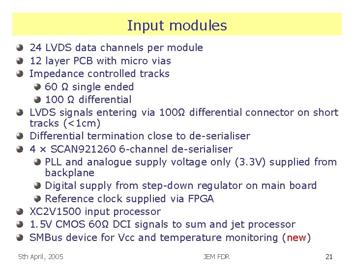
Input modules 24 LVDS data channels per module 12 layer PCB with micro vias Impedance controlled tracks 60 Ω single ended 100 Ω differential LVDS signals entering via 100Ω differential connector on short tracks (<1 cm) Differential termination close to de-serialiser 4 × SCAN 921260 6 -channel de-serialiser PLL and analogue supply voltage only (3. 3 V) supplied from backplane Digital supply from step-down regulator on main board Reference clock supplied via FPGA XC 2 V 1500 input processor 1. 5 V CMOS 60Ω DCI signals to sum and jet processor SMBus device for Vcc and temperature monitoring (new) 5 th April, 2005 JEM FDR 21

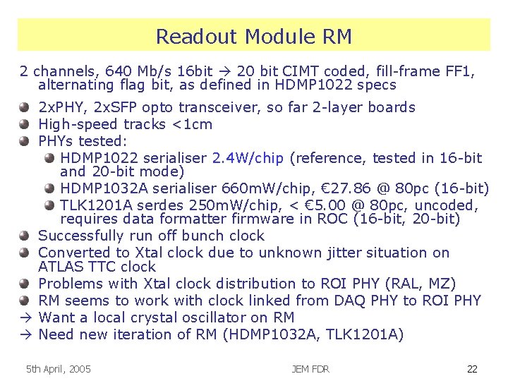
Readout Module RM 2 channels, 640 Mb/s 16 bit 20 bit CIMT coded, fill-frame FF 1, alternating flag bit, as defined in HDMP 1022 specs 2 x. PHY, 2 x. SFP opto transceiver, so far 2 -layer boards High-speed tracks <1 cm PHYs tested: HDMP 1022 serialiser 2. 4 W/chip (reference, tested in 16 -bit and 20 -bit mode) HDMP 1032 A serialiser 660 m. W/chip, € 27. 86 @ 80 pc (16 -bit) TLK 1201 A serdes 250 m. W/chip, < € 5. 00 @ 80 pc, uncoded, requires data formatter firmware in ROC (16 -bit, 20 -bit) Successfully run off bunch clock Converted to Xtal clock due to unknown jitter situation on ATLAS TTC clock Problems with Xtal clock distribution to ROI PHY (RAL, MZ) RM seems to work with clock linked from DAQ PHY to ROI PHY Want a local crystal oscillator on RM Need new iteration of RM (HDMP 1032 A, TLK 1201 A) 5 th April, 2005 JEM FDR 22

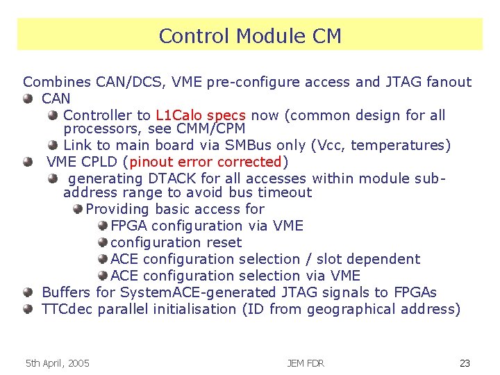
Control Module CM Combines CAN/DCS, VME pre-configure access and JTAG fanout CAN Controller to L 1 Calo specs now (common design for all processors, see CMM/CPM Link to main board via SMBus only (Vcc, temperatures) VME CPLD (pinout error corrected) generating DTACK for all accesses within module subaddress range to avoid bus timeout Providing basic access for FPGA configuration via VME configuration reset ACE configuration selection / slot dependent ACE configuration selection via VME Buffers for System. ACE-generated JTAG signals to FPGAs TTCdec parallel initialisation (ID from geographical address) 5 th April, 2005 JEM FDR 23

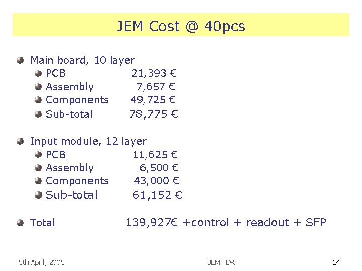
JEM Cost @ 40 pcs Main board, 10 layer PCB 21, 393 € Assembly 7, 657 € Components 49, 725 € Sub-total 78, 775 € Input module, 12 layer PCB 11, 625 € Assembly 6, 500 € Components 43, 000 € Sub-total 61, 152 € Total 5 th April, 2005 139, 927€ +control + readout + SFP JEM FDR 24

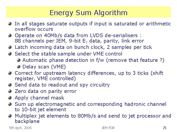
Energy Sum Algorithm In all stages saturate outputs if input is saturated or arithmetic overflow occurs Operate on 40 Mb/s data from LVDS de-serialisers : 88 channels per JEM, 9 -bit ET data, parity, link error Latch incoming data on bunch clock, 2 samples per tick Select the stable sample under VME control Automatic phase detection in f/w (remove that feature ? ) Delay scan (VME) Correct for upstream latency differences, up to 3 ticks (shift register, VME controlled) Send data to readout and spy circuitry Zero data on parity error Apply channel mask Sum up electromagnetic and corresponding hadronic channel to 10 -bit jet element Multiplex jet elements to 80 Mb/s and send to jet processor and backplane 5 th April, 2005 JEM FDR 25

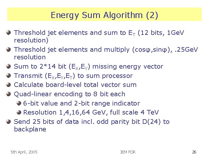
Energy Sum Algorithm (2) Threshold jet elements and sum to ET (12 bits, 1 Ge. V resolution) Threshold jet elements and multiply (cosφ, sinφ), . 25 Ge. V resolution Sum to 2*14 bit (EX, EY) missing energy vector Transmit (EX, EY, ET) to sum processor Calculate board-level total vector sum Quad-linear encoding to 8 bit each 6 -bit value and 2 -bit range indicator Resolution 1, 4, 16, 64 Ge. V, full scale 4 Te. V Send 25 bits of data incl. odd parity bit D(24) to backplane 5 th April, 2005 JEM FDR 26

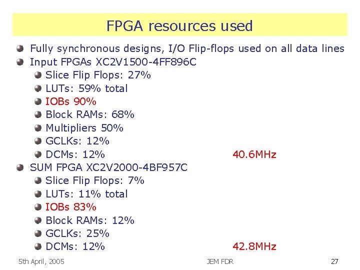
FPGA resources used Fully synchronous designs, I/O Flip-flops used on all data lines Input FPGAs XC 2 V 1500 -4 FF 896 C Slice Flip Flops: 27% LUTs: 59% total IOBs 90% Block RAMs: 68% Multipliers 50% GCLKs: 12% DCMs: 12% 40. 6 MHz SUM FPGA XC 2 V 2000 -4 BF 957 C Slice Flip Flops: 7% LUTs: 11% total IOBs 83% Block RAMs: 12% GCLKs: 25% DCMs: 12% 42. 8 MHz 5 th April, 2005 JEM FDR 27

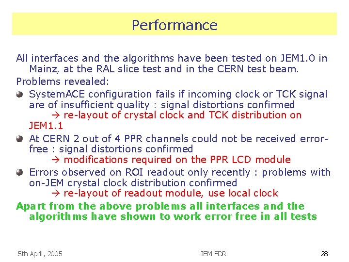
Performance All interfaces and the algorithms have been tested on JEM 1. 0 in Mainz, at the RAL slice test and in the CERN test beam. Problems revealed: System. ACE configuration fails if incoming clock or TCK signal are of insufficient quality : signal distortions confirmed re-layout of crystal clock and TCK distribution on JEM 1. 1 At CERN 2 out of 4 PPR channels could not be received errorfree : signal distortions confirmed modifications required on the PPR LCD module Errors observed on ROI readout only recently : problems with on-JEM crystal clock distribution confirmed re-layout of readout module, use local clock Apart from the above problems all interfaces and the algorithms have shown to work error free in all tests 5 th April, 2005 JEM FDR 28

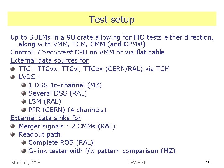
Test setup Up to 3 JEMs in a 9 U crate allowing for FIO tests either direction, along with VMM, TCM, CMM (and CPMs!) Control: Concurrent CPU on VMM or via flat cable External data sources for TTC : TTCvx, TTCvi, TTCex (CERN/RAL) via TCM LVDS : 1 DSS 16 -channel (MZ) Several DSS (RAL) LSM (RAL) PPR (CERN) (4 channels) External data sinks for Merger signals : 2 CMMs (RAL) Readout path: Complete ROS (RAL) G-link tester with f/w pattern comparison (MZ) 5 th April, 2005 JEM FDR 29

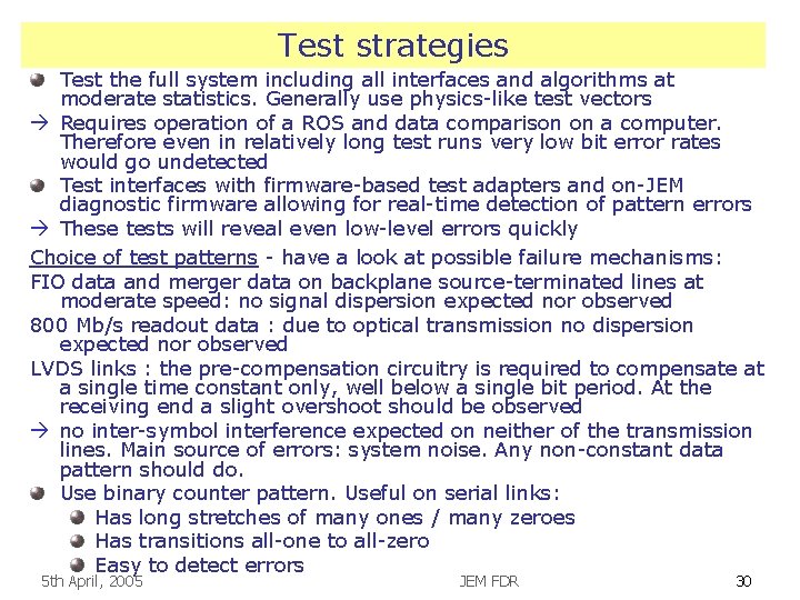
Test strategies Test the full system including all interfaces and algorithms at moderate statistics. Generally use physics-like test vectors Requires operation of a ROS and data comparison on a computer. Therefore even in relatively long test runs very low bit error rates would go undetected Test interfaces with firmware-based test adapters and on-JEM diagnostic firmware allowing for real-time detection of pattern errors These tests will reveal even low-level errors quickly Choice of test patterns - have a look at possible failure mechanisms: FIO data and merger data on backplane source-terminated lines at moderate speed: no signal dispersion expected nor observed 800 Mb/s readout data : due to optical transmission no dispersion expected nor observed LVDS links : the pre-compensation circuitry is required to compensate at a single time constant only, well below a single bit period. At the receiving end a slight overshoot should be observed no inter-symbol interference expected on neither of the transmission lines. Main source of errors: system noise. Any non-constant data pattern should do. Use binary counter pattern. Useful on serial links: Has long stretches of many ones / many zeroes Has transitions all-one to all-zero Easy to detect errors 5 th April, 2005 JEM FDR 30

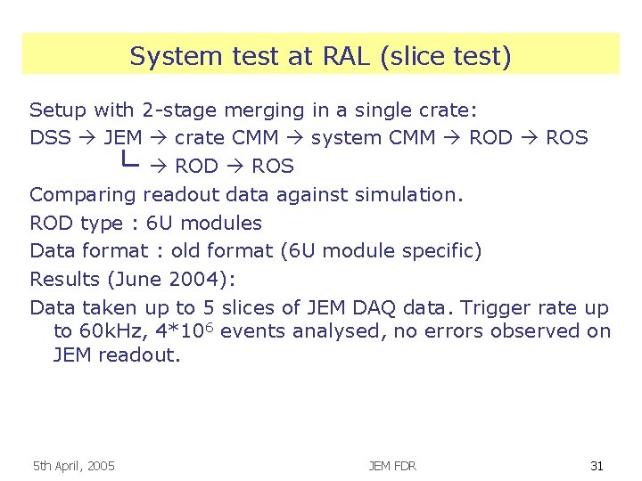
System test at RAL (slice test) Setup with 2 -stage merging in a single crate: DSS JEM crate CMM system CMM ROD ROS Comparing readout data against simulation. ROD type : 6 U modules Data format : old format (6 U module specific) Results (June 2004): Data taken up to 5 slices of JEM DAQ data. Trigger rate up to 60 k. Hz, 4*106 events analysed, no errors observed on JEM readout. 5 th April, 2005 JEM FDR 31

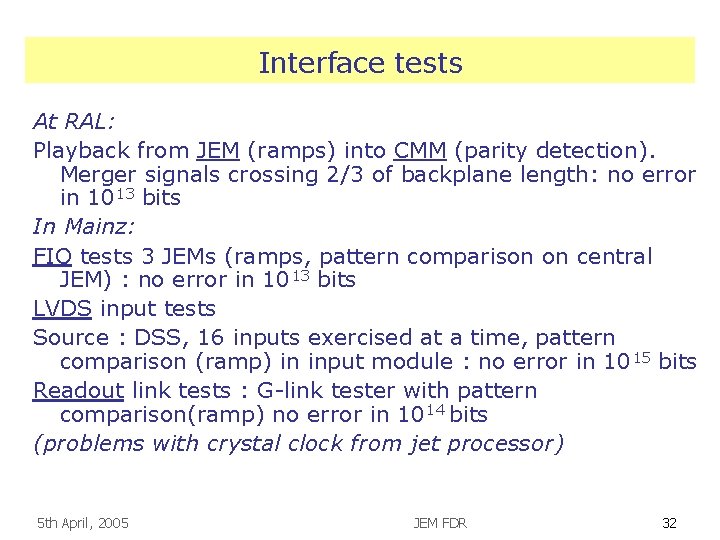
Interface tests At RAL: Playback from JEM (ramps) into CMM (parity detection). Merger signals crossing 2/3 of backplane length: no error in 1013 bits In Mainz: FIO tests 3 JEMs (ramps, pattern comparison on central JEM) : no error in 1013 bits LVDS input tests Source : DSS, 16 inputs exercised at a time, pattern comparison (ramp) in input module : no error in 1015 bits Readout link tests : G-link tester with pattern comparison(ramp) no error in 1014 bits (problems with crystal clock from jet processor) 5 th April, 2005 JEM FDR 32

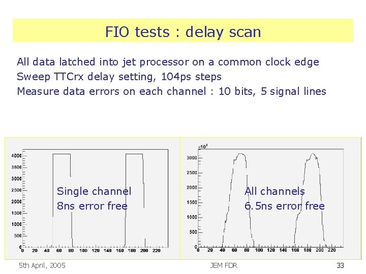
FIO tests : delay scan All data latched into jet processor on a common clock edge Sweep TTCrx delay setting, 104 ps steps Measure data errors on each channel : 10 bits, 5 signal lines Single channel 8 ns error free 5 th April, 2005 All channels 6. 5 ns error free JEM FDR 33

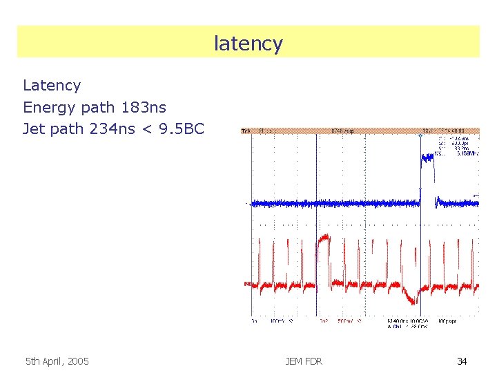
latency Latency Energy path 183 ns Jet path 234 ns < 9. 5 BC 5 th April, 2005 JEM FDR 34

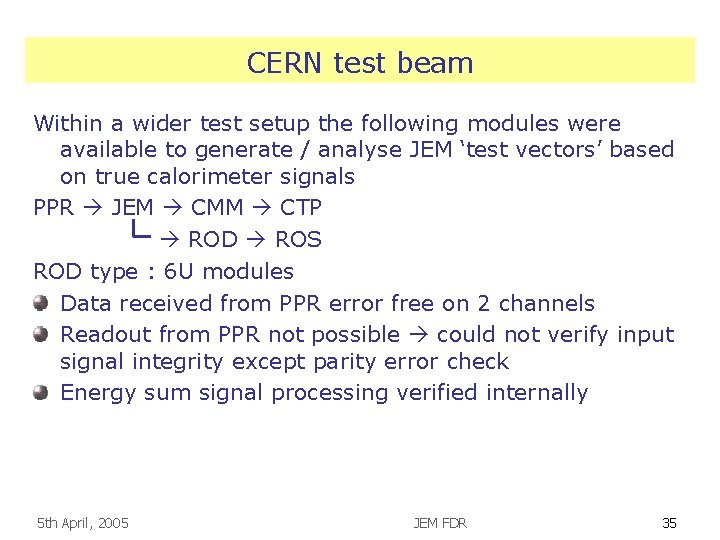
CERN test beam Within a wider test setup the following modules were available to generate / analyse JEM ‘test vectors’ based on true calorimeter signals PPR JEM CMM CTP ROD ROS ROD type : 6 U modules Data received from PPR error free on 2 channels Readout from PPR not possible could not verify input signal integrity except parity error check Energy sum signal processing verified internally 5 th April, 2005 JEM FDR 35

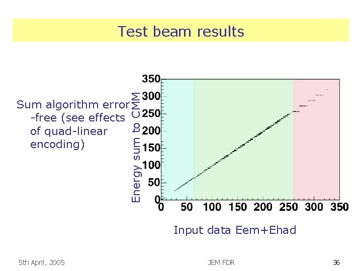
Energy sum to CMM Test beam results Sum algorithm error -free (see effects of quad-linear encoding) Input data Eem+Ehad 5 th April, 2005 JEM FDR 36

Production tests Boundary scan at manufacturer: high coverage due to large fraction of scannable components verify connectivity (static test) Standalone tester for input module LVDS inputs, pattern comparison in firmware (high statistics) Standalone tester for readout module, pattern comparison in firmware (high statistics) DCI operation verified w. oscilloscope (drive unterminated 50 Ω cable into scope, record pulse shape) dynamic test System-level tests in Mainz : 1 crate, 1 JEM supplied with LVDS data at a time, playback and spy facilities used to generate / capture data on board boundaries. FIO delay scan High statistics FIO BER tests, pattern detection in firmware, test full crate at a time with maximum activity on LVDS, VME, readout System-level tests at CERN 5 th April, 2005 JEM FDR 37