JEM Status and plans Hardware JEM 1 Status
- Slides: 7

JEM Status and plans • Hardware - JEM 1 - Status • Firmware - Algorithms - Status • Plans Uli Schäfer 1

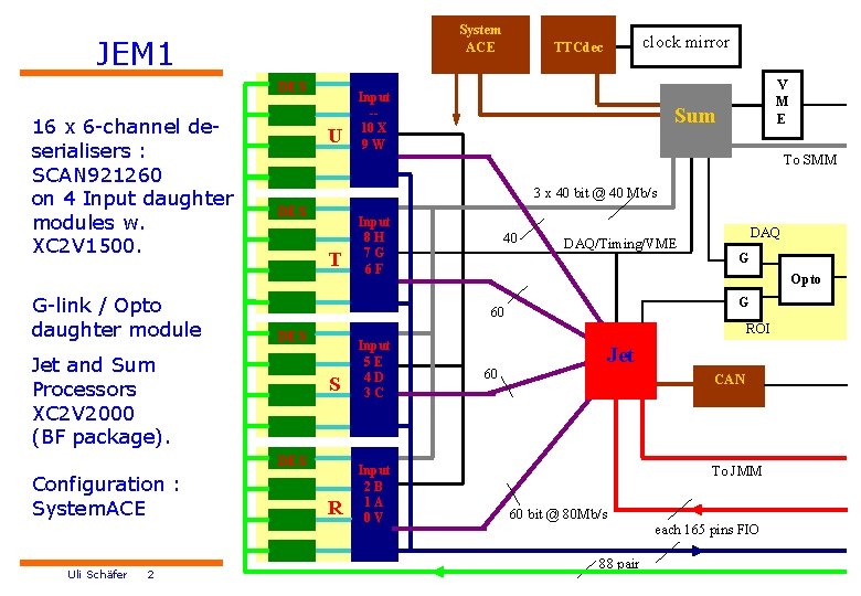
System ACE JEM 1 DES 16 x 6 -channel deserialisers : SCAN 921260 on 4 Input daughter modules w. XC 2 V 1500. G-link / Opto daughter module U DES T 2 V M E Sum To SMM Input 8 H 7 G 6 F 40 DAQ/Timing/VME DAQ G Opto G 60 ROI DES S DES Uli Schäfer Input -10 X 9 W 3 x 40 bit @ 40 Mb/s Jet and Sum Processors XC 2 V 2000 (BF package). Configuration : System. ACE clock mirror TTCdec R Input 5 E 4 D 3 C Input 2 B 1 A 0 V 60 Jet CAN To JMM 60 bit @ 80 Mb/s 88 pair each 165 pins FIO

JEM 1 main board Components : • Backplane and daughter connectors (TTC, input, G-link) • Bus drivers (VME) and PECL line drivers/receivers • Jet and Sum processors (BGA 1. 28 mm pitch) • 2 CPLDs (VME / display) • Front panel connectors/LEDs • System. ACE configurator / flash chip • CAN • Voltage converters Production: One-stop Rohde & Schwarz • Component procurement • PCB production • Adjustment of impedances • Test protocols • Assembly • Visual inspection • X-ray Uli Schäfer 3

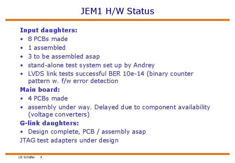
JEM 1 H/W Status Input daughters: • 8 PCBs made • 1 assembled • 3 to be assembled asap • stand-alone test system set up by Andrey • LVDS link tests successful BER 10 e-14 (binary counter pattern w. f/w error detection Main board: • 4 PCBs made • assembly under way. Delayed due to component availability (voltage converters) G-link daughters: • Design complete, PCB / assembly asap JTAG test adapters under design Uli Schäfer 4

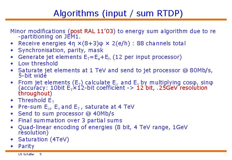
Algorithms (input / sum RTDP) Minor modifications (post RAL 11’ 03) to energy sum algorithm due to re -partitioning on JEM 1. • Receive energies 4η ×(8+3)φ × 2(e/h) : 88 channels total • Synchronisation, parity, mask • Generate jet elements ET=Ee+Eh (12 per input processor) • Low threshold • Saturate jet elements at 1 Te. V and send to jet processor @ 80 Mb/s, 5 -bit wide • From jet elements (ET) calculate EX and EY by multiplying cosφ, sinφ (accuracy: 10 bit ET× 12 -bit coefficient -> 12 bit, . 25 Ge. V resolution throughout) • Threshold ET • Pre-sum EX, EY and ET , saturate at 4 Te. V • Send to sum processor @ 40 Mb/s • Final summation over 3 partial sums • Quad-linear encoding of energies (8 bit, 4 Te. V range, 1 Ge. V resolution) • Saturation (4 Te. V) • Parity Uli Schäfer 5

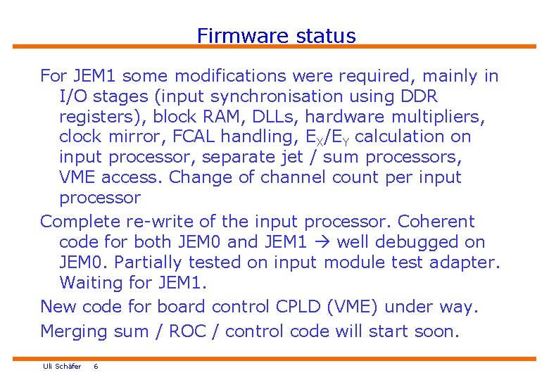
Firmware status For JEM 1 some modifications were required, mainly in I/O stages (input synchronisation using DDR registers), block RAM, DLLs, hardware multipliers, clock mirror, FCAL handling, EX/EY calculation on input processor, separate jet / sum processors, VME access. Change of channel count per input processor Complete re-write of the input processor. Coherent code for both JEM 0 and JEM 1 well debugged on JEM 0. Partially tested on input module test adapter. Waiting for JEM 1. New code for board control CPLD (VME) under way. Merging sum / ROC / control code will start soon. Uli Schäfer 6

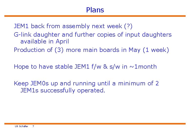
Plans JEM 1 back from assembly next week (? ) G-link daughter and further copies of input daughters available in April Production of (3) more main boards in May (1 week) Hope to have stable JEM 1 f/w & s/w in ~1 month Keep JEM 0 s up and running until a minimum of 2 JEM 1 s successfully operated. Uli Schäfer 7