JEM Status and plans Algorithms Hardware JEM 0
- Slides: 10

JEM Status and plans • Algorithms • Hardware JEM 0, JEM 1 • Tests • Plans Uli Schäfer

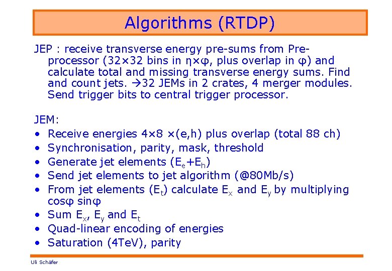
Algorithms (RTDP) JEP : receive transverse energy pre-sums from Preprocessor (32× 32 bins in η×φ, plus overlap in φ) and calculate total and missing transverse energy sums. Find and count jets. 32 JEMs in 2 crates, 4 merger modules. Send trigger bits to central trigger processor. JEM: • Receive energies 4× 8 ×(e, h) plus overlap (total 88 ch) • Synchronisation, parity, mask, threshold • Generate jet elements (Ee+Eh) • Send jet elements to jet algorithm (@80 Mb/s) • From jet elements (Et) calculate Ex and Ey by multiplying cosφ sinφ • Sum Ex, Ey and Et • Quad-linear encoding of energies • Saturation (4 Te. V), parity Uli Schäfer

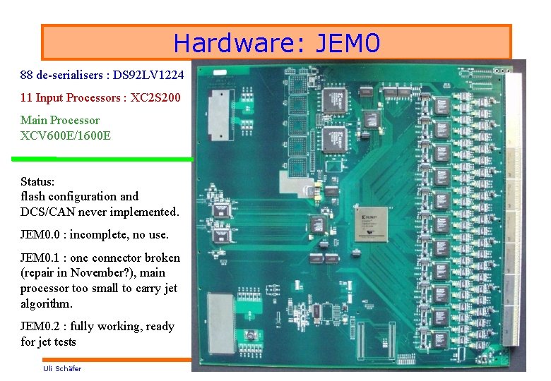
Hardware: JEM 0 88 de-serialisers : DS 92 LV 1224 11 Input Processors : XC 2 S 200 Main Processor XCV 600 E/1600 E Status: flash configuration and DCS/CAN never implemented. JEM 0. 0 : incomplete, no use. JEM 0. 1 : one connector broken (repair in November? ), main processor too small to carry jet algorithm. JEM 0. 2 : fully working, ready for jet tests Uli Schäfer

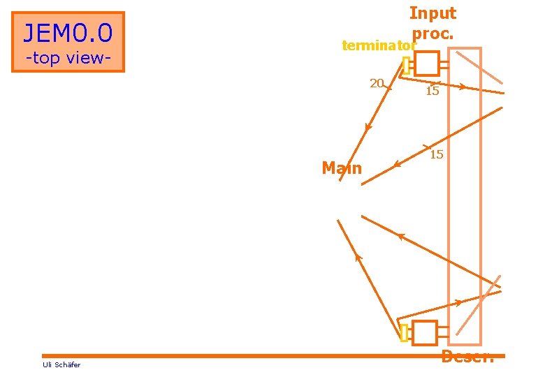
JEM 0. 0 -top view- Input proc. terminator 20 Main Uli Schäfer 15 15 Deser.

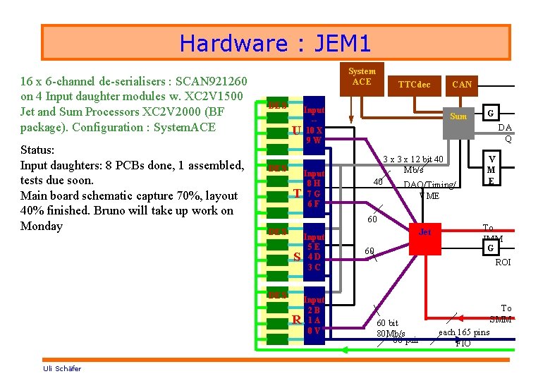
Hardware : JEM 1 16 x 6 -channel de-serialisers : SCAN 921260 on 4 Input daughter modules w. XC 2 V 1500 Jet and Sum Processors XC 2 V 2000 (BF package). Configuration : System. ACE Status: Input daughters: 8 PCBs done, 1 assembled, tests due soon. Main board schematic capture 70%, layout 40% finished. Bruno will take up work on Monday System ACE DES T Input 8 H 7 G 6 F Sum DES Input 5 E 4 D 3 C Input 2 B R 1 A 0 V G DA Q 3 x 12 bit 40 Mb/s 40 DAQ/Timing/ VME 60 DES CAN Input -U 10 X 9 W S Uli Schäfer TTCdec Jet 60 V M E To JMM G ROI 60 bit 80 Mb/s 88 pair To SMM each 165 pins FIO

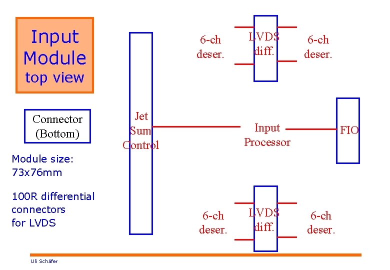
Input Module 6 -ch deser. LVDS diff. 6 -ch deser. top view Connector (Bottom) Jet Sum Control Input Processor FIO Module size: 73 x 76 mm 100 R differential connectors for LVDS Uli Schäfer 6 -ch deser. LVDS diff. 6 -ch deser.

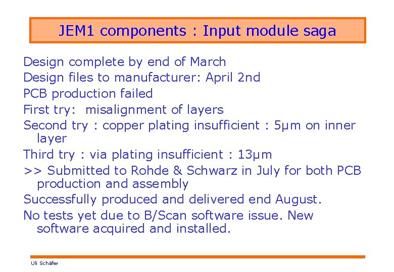
JEM 1 components : Input module saga Design complete by end of March Design files to manufacturer: April 2 nd PCB production failed First try: misalignment of layers Second try : copper plating insufficient : 5μm on inner layer Third try : via plating insufficient : 13μm >> Submitted to Rohde & Schwarz in July for both PCB production and assembly Successfully produced and delivered end August. No tests yet due to B/Scan software issue. New software acquired and installed. Uli Schäfer

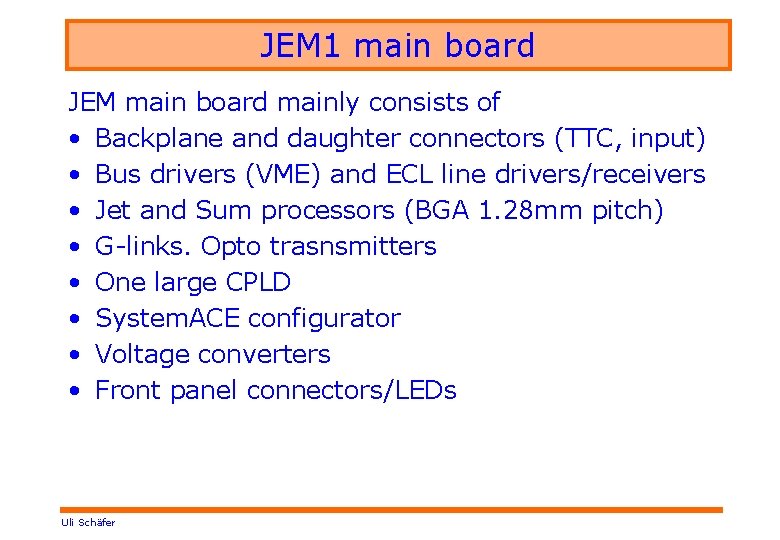
JEM 1 main board JEM main board mainly consists of • Backplane and daughter connectors (TTC, input) • Bus drivers (VME) and ECL line drivers/receivers • Jet and Sum processors (BGA 1. 28 mm pitch) • G-links. Opto trasnsmitters • One large CPLD • System. ACE configurator • Voltage converters • Front panel connectors/LEDs Uli Schäfer

Firmware / test For JEM 1 some modifications are required, mainly in I/O stages (DDR registers), block RAM, DLLs, hardware multipliers, clock mirror, FCAL handling, Ex/Ey calculation on input processor, separate sum processor, VME access. Change of channel count per input processor Work started : complete re-write of input processor, since previous version was hard-wired for 8 channels, instantiations, no loops. Coherent code for both JEM 0 and JEM 1 debug on JEM 0 and hope for plug and play once JEM 1 arrives VME register map completely refurbished adapt on-line software ! Separate test bench w. Windows PC, JEM 0. 1, configuration via JTAG, data transmission through printer port. Use this test setup for early tests of JEM 1 input processor (Andrey) Uli Schäfer

Plans / to do Hardware (Bruno/Uli): • Boundary Scan of input daughter • Input processor test module • Finish JEM 1 design and submit All to be done by end 2003, pay from 2003 CORE money! Firmware (Uli): • Complete JEM 1 compatible firmware (stable Jan. 2004? ) Software: (Cano, Andrey, Thomas) • adapt to JEM 1 (? ) • Look into PVSS / OPC /CAN (not CANopen!) (Andrey) • ? ? Tests (All) • Mainz remote jet test in November? • RAL test in November? – ROD tests – CMM tests – Full jet code tests (2 JEMs ? Need re-work!) • Input daughter test (Andrey) Uli Schäfer