JEM Status and plans Hardware status JEM 0
- Slides: 11

JEM Status and plans • Hardware status JEM 0 • Hardware status JEM 1 • Plans Uli Schäfer

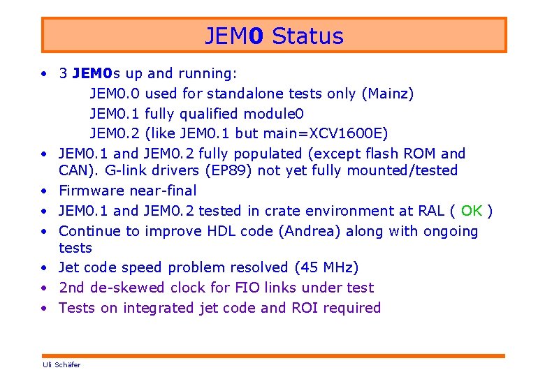
JEM 0 Status • 3 JEM 0 s up and running: JEM 0. 0 used for standalone tests only (Mainz) JEM 0. 1 fully qualified module 0 JEM 0. 2 (like JEM 0. 1 but main=XCV 1600 E) • JEM 0. 1 and JEM 0. 2 fully populated (except flash ROM and CAN). G-link drivers (EP 89) not yet fully mounted/tested • Firmware near-final • JEM 0. 1 and JEM 0. 2 tested in crate environment at RAL ( OK ) • Continue to improve HDL code (Andrea) along with ongoing tests • Jet code speed problem resolved (45 MHz) • 2 nd de-skewed clock for FIO links under test • Tests on integrated jet code and ROI required Uli Schäfer

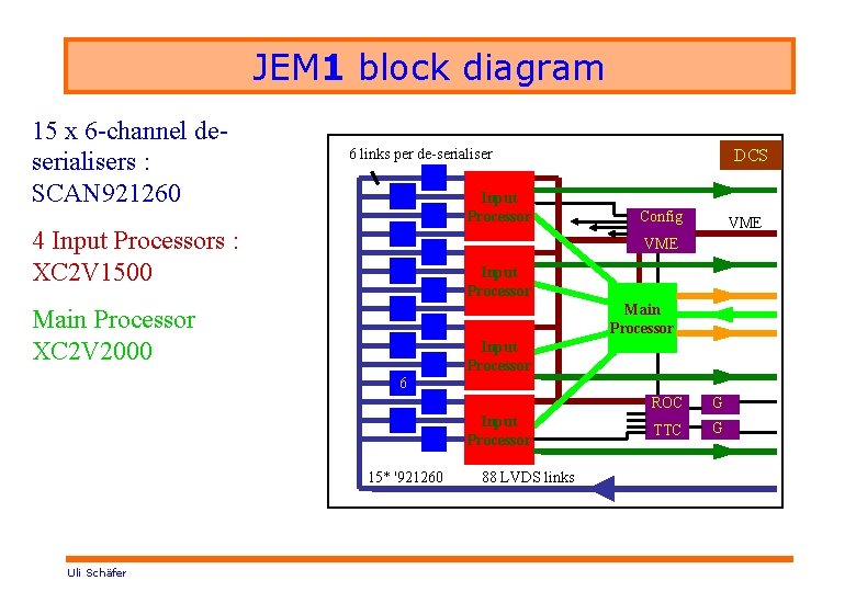
JEM 1 block diagram 15 x 6 -channel deserialisers : SCAN 921260 6 links per de-serialiser Input Processor 4 Input Processors : XC 2 V 1500 DCS Config VME Input Processor Main Processor XC 2 V 2000 Input Processor 6 Input Processor 15* '921260 Uli Schäfer 88 LVDS links ROC G TTC G

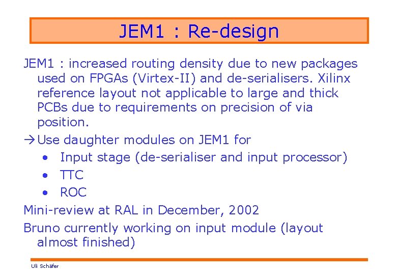
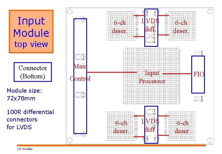
JEM 1 : Re-design JEM 1 : increased routing density due to new packages used on FPGAs (Virtex-II) and de-serialisers. Xilinx reference layout not applicable to large and thick PCBs due to requirements on precision of via position. Use daughter modules on JEM 1 for • Input stage (de-serialiser and input processor) • TTC • ROC Mini-review at RAL in December, 2002 Bruno currently working on input module (layout almost finished) Uli Schäfer

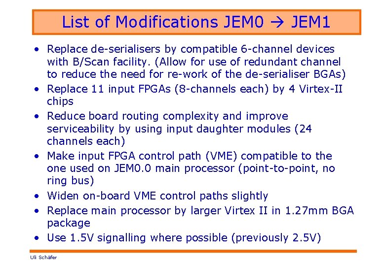
List of Modifications JEM 0 JEM 1 • Replace de-serialisers by compatible 6 -channel devices with B/Scan facility. (Allow for use of redundant channel to reduce the need for re-work of the de-serialiser BGAs) • Replace 11 input FPGAs (8 -channels each) by 4 Virtex-II chips • Reduce board routing complexity and improve serviceability by using input daughter modules (24 channels each) • Make input FPGA control path (VME) compatible to the one used on JEM 0. 0 main processor (point-to-point, no ring bus) • Widen on-board VME control paths slightly • Replace main processor by larger Virtex II in 1. 27 mm BGA package • Use 1. 5 V signalling where possible (previously 2. 5 V) Uli Schäfer

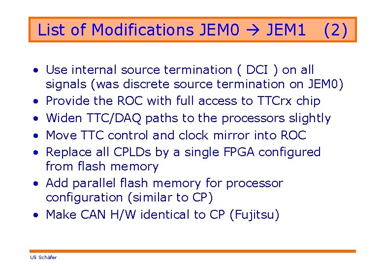
List of Modifications JEM 0 JEM 1 (2) • Use internal source termination ( DCI ) on all signals (was discrete source termination on JEM 0) • Provide the ROC with full access to TTCrx chip • Widen TTC/DAQ paths to the processors slightly • Move TTC control and clock mirror into ROC • Replace all CPLDs by a single FPGA configured from flash memory • Add parallel flash memory for processor configuration (similar to CP) • Make CAN H/W identical to CP (Fujitsu) Uli Schäfer

Input Module 6 -ch deser. LVDS diff. 6 -ch deser. top view Connector (Bottom) Main Input Processor Control FIO Module size: 72 x 78 mm 100 R differential connectors for LVDS Uli Schäfer 6 -ch deser. LVDS diff. 6 -ch deser.

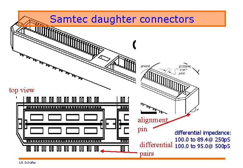
Samtec daughter connectors top view alignment pin differential pairs Uli Schäfer differential impedance: 100. 0 to 89. 4@ 250 p. S 100. 0 to 95. 0@ 500 p. S

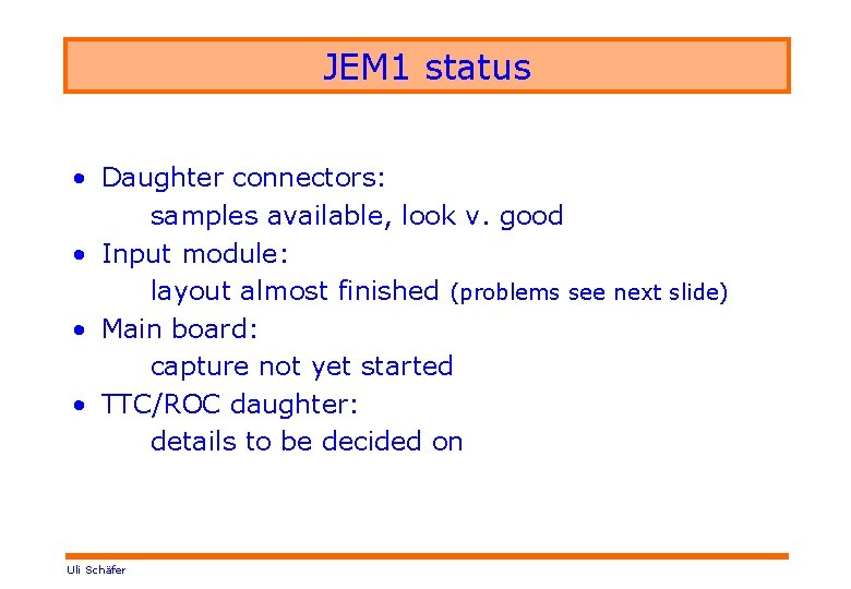
JEM 1 status • Daughter connectors: samples available, look v. good • Input module: layout almost finished (problems see next slide) • Main board: capture not yet started • TTC/ROC daughter: details to be decided on Uli Schäfer

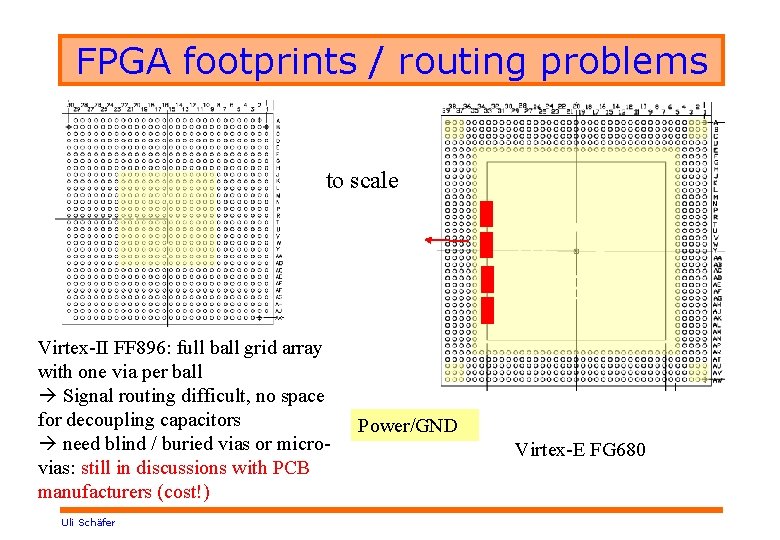
FPGA footprints / routing problems to scale Virtex-II FF 896: full ball grid array with one via per ball Signal routing difficult, no space for decoupling capacitors need blind / buried vias or microvias: still in discussions with PCB manufacturers (cost!) Uli Schäfer Power/GND Virtex-E FG 680

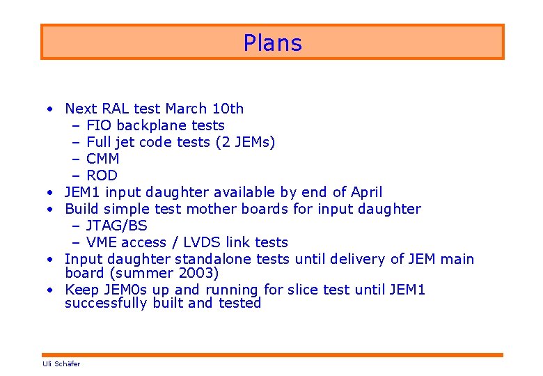
Plans • Next RAL test March 10 th – FIO backplane tests – Full jet code tests (2 JEMs) – CMM – ROD • JEM 1 input daughter available by end of April • Build simple test mother boards for input daughter – JTAG/BS – VME access / LVDS link tests • Input daughter standalone tests until delivery of JEM main board (summer 2003) • Keep JEM 0 s up and running for slice test until JEM 1 successfully built and tested Uli Schäfer