Introduction to Electronics for High Energy Physics CERN
- Slides: 23

Introduction to Electronics for High Energy Physics CERN Summer school 2003 C. de LA TAILLE LAL Orsay 9 -11 july 2003 C. de La Taille@lal. in 2 p 3. fr Electronics CERN Summer School 2003 1

Outline n Course 1 : The art of electronics : is there something beyond Ohm’s law ? n Course 2 : Learning to decipher a schematic n Course 3 : Electronics in high energy physics 9 -11 july 2003 C. de La Taille Electronics CERN Summer School 2003 2

Introduction n Speak “electronician” in just 3 lessons… “Did you cascode your charge preamp to increase your open loop gain ? ” n “Did you find an FPGA with LVDS I/Os for your digital filter ? ” n A lot of vocabulary (and abreviations…) to get used to, but : n n Little prerequisite knowledge required : Ohm’s law : U = Z I n Some basics of Fourier (or Laplace) transforms cannot hurt for signal theory n n Many more details are given in the transparencies -> don’t be scared ! 9 -11 july 2003 C. de La Taille Electronics CERN Summer School 2003 3

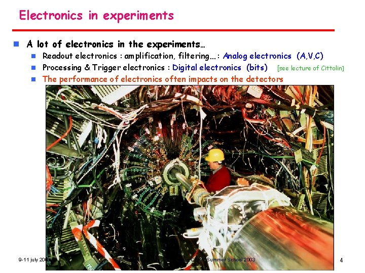
Electronics in experiments n A lot of electronics in the experiments… Readout electronics : amplification, filtering… : Analog electronics (A, V, C) n Processing & Trigger electronics : Digital electronics (bits) [see lecture of Cittolin] n The performance of electronics often impacts on the detectors n 9 -11 july 2003 C. de La Taille Electronics CERN Summer School 2003 4

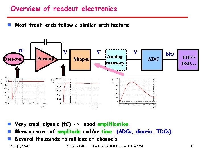
Overview of readout electronics n Most front-ends follow a similar architecture f. C Detector V Preamp V Shaper Analog memory V ADC bits FIFO DSP… n Very small signals (f. C) -> need amplification n Measurement of amplitude and/or time (ADCs, discris, TDCs) n Several thousands to millions of channels 9 -11 july 2003 C. de La Taille Electronics CERN Summer School 2003 5

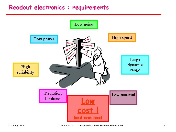
Readout electronics : requirements Low noise High speed Low power Large dynamic range High reliability Radiation hardness Low cost ! Low material (and even less) 9 -11 july 2003 C. de La Taille Electronics CERN Summer School 2003 6

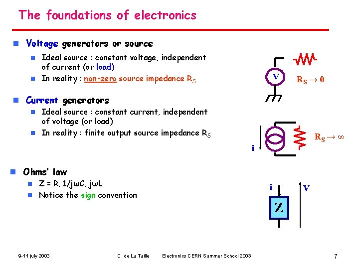
The foundations of electronics n Voltage generators or source Ideal source : constant voltage, independent of current (or load) n In reality : non-zero source impedance RS n V RS → 0 n Current generators Ideal source : constant current, independent of voltage (or load) n In reality : finite output source impedance RS n RS → ∞ i n Ohms’ law Z = R, 1/jωC, jωL n Notice the sign convention n 9 -11 july 2003 C. de La Taille i V Z Electronics CERN Summer School 2003 7

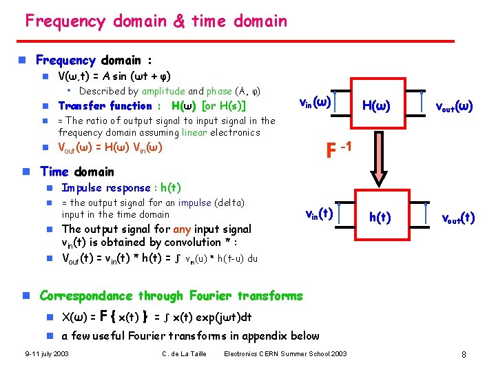
Frequency domain & time domain n Frequency domain : n V(ω, t) = A sin (ωt + φ) • Described by amplitude and phase (A, φ) n Transfer function : H(ω) [or H(s)] n = The ratio of output signal to input signal in the frequency domain assuming linear electronics n Vout(ω) = H(ω) Vin(ω) vin(ω) H(ω) vout(ω) h(t) vout(t) F -1 n Time domain n Impulse response : h(t) n = the output signal for an impulse (delta) input in the time domain The output signal for any input signal vin(t) is obtained by convolution * : n Vout(t) = vin(t) * h(t) = ∫ vin(u) * h(t-u) du vin(t) n n Correspondance through Fourier transforms n X(ω) = F { x(t) } = ∫ x(t) exp(jωt)dt n a few useful Fourier transforms in appendix below 9 -11 july 2003 C. de La Taille Electronics CERN Summer School 2003 8

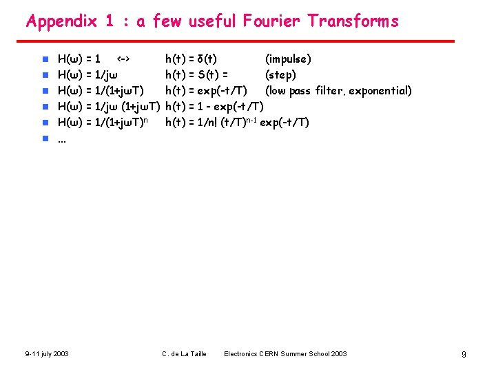
Appendix 1 : a few useful Fourier Transforms n n n H(ω) = 1 <-> H(ω) = 1/jω H(ω) = 1/(1+jωT) H(ω) = 1/jω (1+jωT) H(ω) = 1/(1+jωT)n … 9 -11 july 2003 h(t) = δ(t) (impulse) h(t) = S(t) = (step) h(t) = exp(-t/T) (low pass filter, exponential) h(t) = 1 - exp(-t/T) h(t) = 1/n! (t/T)n-1 exp(-t/T) C. de La Taille Electronics CERN Summer School 2003 9

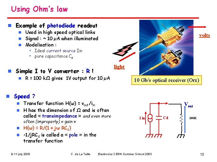
Using Ohm’s law n Example of photodiode readout Used in high speed optical links n Signal : ~ 10 µA when illuminated n Modelisation : n volts • Ideal current source Iin • pure capacitance Cd light n Simple I to V converter : R ! n R = 100 kΩ gives 1 V output for 10 µA 10 Gb/s optical receiver (Orx) n Speed ? Transfer function H(ω) = vout/iin n H has the dimension of Ω and is often called « transimpedance » and even more Vout n often (improperly) « gain » I in Cd 100 K H(ω) = R/(1 + jω RCd) n -1/j. RCd is called a « pole » in the transfer function n 9 -11 july 2003 C. de La Taille Electronics CERN Summer School 2003 10

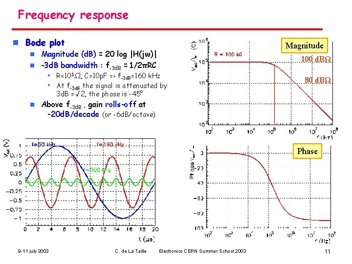
Frequency response n Bode plot Magnitude (d. B) = 20 log |H(jw)| n -3 d. B bandwidth : f-3 d. B = 1/2πRC n 100 d. BΩ • R=105Ω, C=10 p. F => f-3 d. B=160 k. Hz • At f-3 d. B the signal is attenuated by 3 d. B = √ 2, the phase is -45° n 80 d. BΩ Above f-3 d. B , gain rolls-off at -20 d. B/decade (or -6 d. B/octave) Phase 9 -11 july 2003 C. de La Taille Electronics CERN Summer School 2003 11

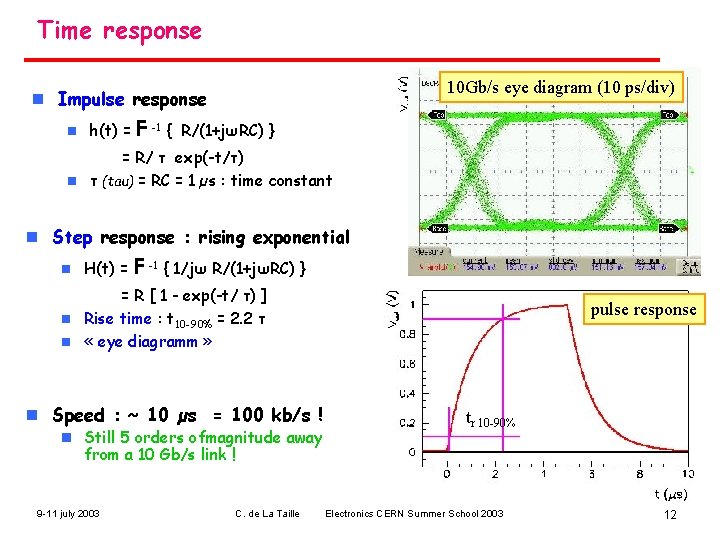
Time response 10 Gb/s eye diagram ps/div) Impulse(10 response n Impulse response n h(t) = F -1 { R/(1+jωRC) } = R/ τ exp(-t/τ) n τ (tau) = RC = 1 µs : time constant n Step response : rising exponential n H(t) = F -1 { 1/jω R/(1+jωRC) } = R [ 1 - exp(-t/ τ) ] n Rise time : t 10 -90% = 2. 2 τ n « eye diagramm » n Speed : ~ 10 µs = 100 kb/s ! n Still 5 orders ofmagnitude away from a 10 Gb/s link ! 9 -11 july 2003 C. de La Taille pulse response tr 10 -90% Electronics CERN Summer School 2003 12

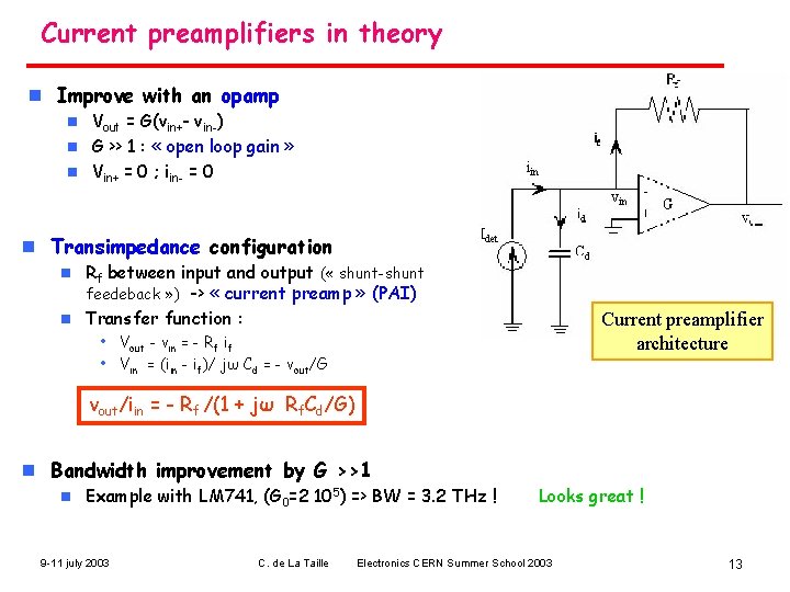
Current preamplifiers in theory n Improve with an opamp Vout = G(vin+- vin-) n G >> 1 : « open loop gain » n Vin+ = 0 ; iin- = 0 n n Transimpedance configuration Rf between input and output ( « shunt-shunt feedeback » ) -> « current preamp » (PAI) n Transfer function : n Current preamplifier architecture • Vout - vin = - Rf if • Vin = (iin - if)/ jω Cd = - vout/G vout/iin = - Rf /(1 + jω Rf. Cd/G) n Bandwidth improvement by G >>1 n Example with LM 741, (G 0=2 105) => BW = 3. 2 THz ! 9 -11 july 2003 C. de La Taille Looks great ! Electronics CERN Summer School 2003 13

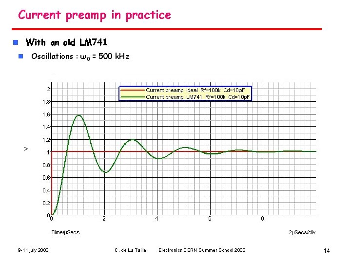
Current preamp in practice n With an old LM 741 n Oscillations : ω0 = 500 k. Hz 9 -11 july 2003 C. de La Taille Electronics CERN Summer School 2003 14

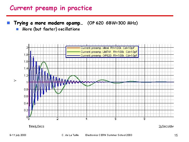
Current preamp in practice n Trying a more modern opamp… (OP 620 GBW=300 MHz) n More (but faster) oscillations 9 -11 july 2003 C. de La Taille Electronics CERN Summer School 2003 15

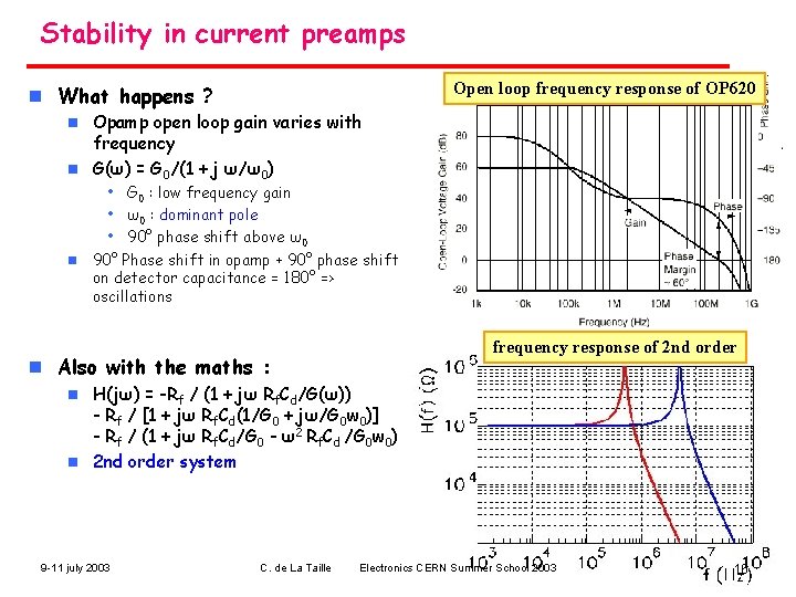
Stability in current preamps Open loop frequency response of OP 620 n What happens ? Opamp open loop gain varies with frequency n G(ω) = G 0/(1 + j ω/ω0) n • G 0 : low frequency gain • ω0 : dominant pole • 90° phase shift above ω0 n 90° Phase shift in opamp + 90° phase shift on detector capacitance = 180° => oscillations frequency response of 2 nd order n Also with the maths : H(jω) = -Rf / (1 + jω Rf. Cd/G(ω)) - Rf / [1 + jω Rf. Cd(1/G 0 + jω/G 0 w 0)] - Rf / (1 + jω Rf. Cd/G 0 - ω2 Rf. Cd /G 0 w 0) n 2 nd order system n 9 -11 july 2003 C. de La Taille = = Electronics CERN Summer School 2003 16

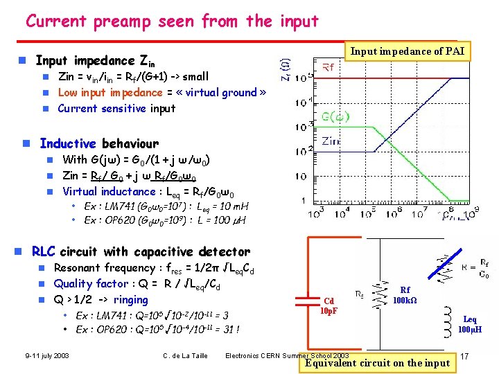
Current preamp seen from the input Input impedance of PAI n Input impedance Zin = vin/iin = Rf/(G+1) -> small n Low input impedance = « virtual ground » n Current sensitive input n n Inductive behaviour With G(jω) = G 0/(1 + j ω/ω0) n Zin = Rf/ G 0 + j ω Rf/G 0ω0 n Virtual inductance : Leq = Rf/G 0ω0 n • Ex : LM 741 (G 0ω0=107) : Leq = 10 m. H • Ex : OP 620 (G 0ω0=109) : L = 100 µH n RLC circuit with capacitive detector Resonant frequency : fres = 1/2π √Leq. Cd n Quality factor : Q = R / √Leq/Cd n Q > 1/2 -> ringing • Ex : LM 741 : Q=105 √ 10 -2/10 -11 = 3 • Ex : OP 620 : Q=105 √ 10 -4/10 -11 = 31 ! n 9 -11 july 2003 C. de La Taille Cd 10 p. F Electronics CERN Summer School 2003 Rf 100 kΩ Equivalent circuit on the input Leq 100µH 17

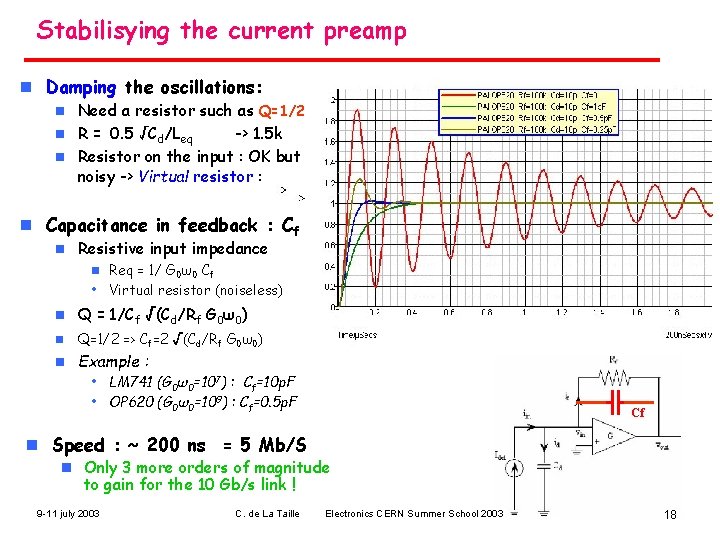
Stabilisying the current preamp n Damping the oscillations: Need a resistor such as Q=1/2 n R = 0. 5 √Cd/Leq -> 1. 5 k n Resistor on the input : OK but noisy -> Virtual resistor : n n Capacitance in feedback : Cf n Resistive input impedance n Req = 1/ G 0ω0 Cf • Virtual resistor (noiseless) Q = 1/Cf √(Cd/Rf G 0ω0) n Q=1/2 => Cf=2 √(Cd/Rf G 0ω0) n Example : n • LM 741 (G 0ω0=107) : Cf=10 p. F • OP 620 (G 0ω0=109) : Cf=0. 5 p. F Cf n Speed : ~ 200 ns = 5 Mb/S n Only 3 more orders of magnitude to gain for the 10 Gb/s link ! 9 -11 july 2003 C. de La Taille Electronics CERN Summer School 2003 18

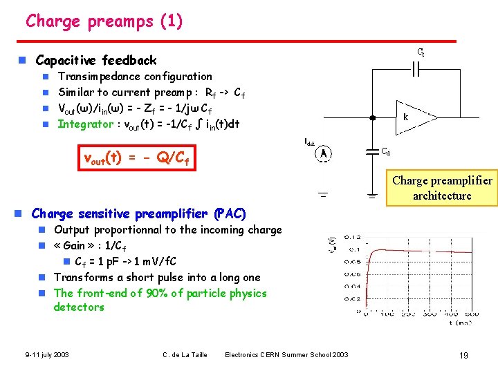
Charge preamps (1) n Capacitive feedback Transimpedance configuration n Similar to current preamp : Rf -> Cf n Vout(ω)/iin(ω) = - Zf = - 1/jω Cf n Integrator : vout(t) = -1/Cf ∫ iin(t)dt n vout(t) = - Q/Cf Charge preamplifier architecture n Charge sensitive preamplifier (PAC) n Output proportionnal to the incoming charge n « Gain » : 1/Cf n Cf = 1 p. F -> 1 m. V/f. C n Transforms a short pulse into a long one n The front-end of 90% of particle physics detectors 9 -11 july 2003 C. de La Taille Electronics CERN Summer School 2003 19

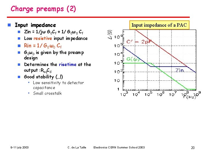
Charge preamps (2) n Input impedance of a PAC Zin = 1/jω G 0 Cf + 1/ G 0ω0 Cf n Low resistive input impedance n n Rin = 1/ G 0ω0 Cf G 0ω0 is given by the preamp design n Determines the risetime at the output : Req. Cd n Good stability (…!) n • Low sensitivity to detector capacitance • Small crosstalk 9 -11 july 2003 C. de La Taille Electronics CERN Summer School 2003 20

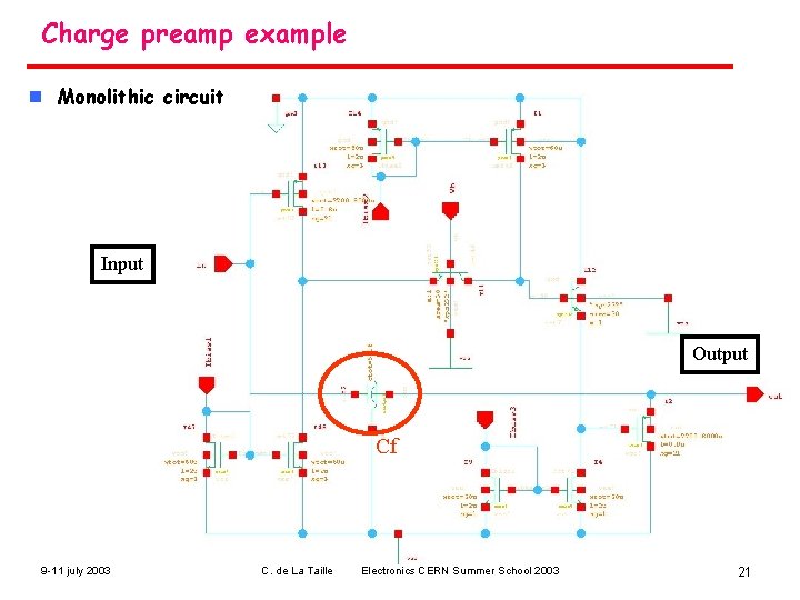
Charge preamp example n Monolithic circuit Input Output Cf 9 -11 july 2003 C. de La Taille Electronics CERN Summer School 2003 21

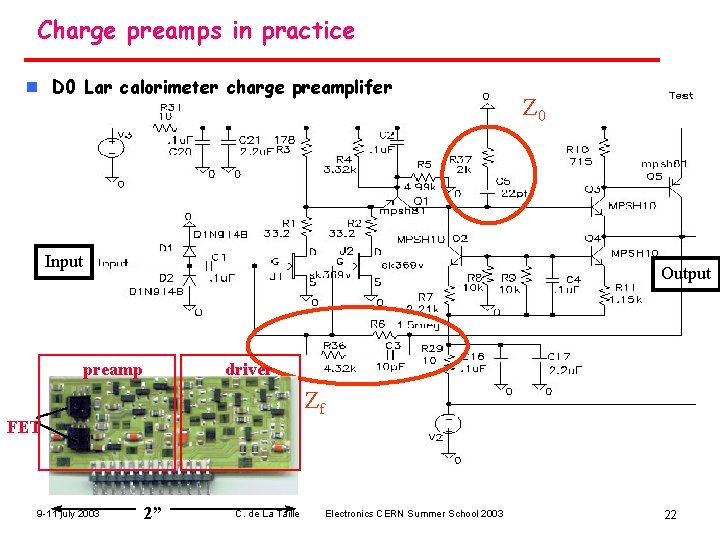
Charge preamps in practice n D 0 Lar calorimeter charge preamplifer Input Z 0 Output preamp driver Zf FET 9 -11 july 2003 2” C. de La Taille Electronics CERN Summer School 2003 22

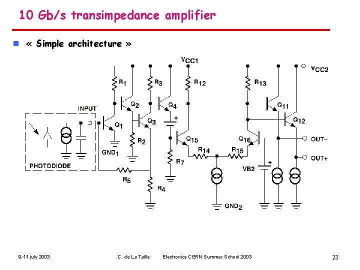
10 Gb/s transimpedance amplifier n « Simple architecture » 9 -11 july 2003 C. de La Taille Electronics CERN Summer School 2003 23