Interconnect and Packaging Lecture 8 Clock Meshes and
- Slides: 25

Interconnect and Packaging Lecture 8: Clock Meshes and Shunts Chung-Kuan Cheng UC San Diego 1

I. Clock Meshes • In Engineering practice, very deep balanced buffer tree + mesh is widely adopted for global clock distribution • IBM Power 4: 64 by 64 grid at the bottom of an Htree • Intel IA: clock stripe at the bottom of a buffer tree. • “Skew Averaging”: shunt at different levels • “Skew Averaging Factor” determined by simulation. No guideline for routing resource planning known yet 2

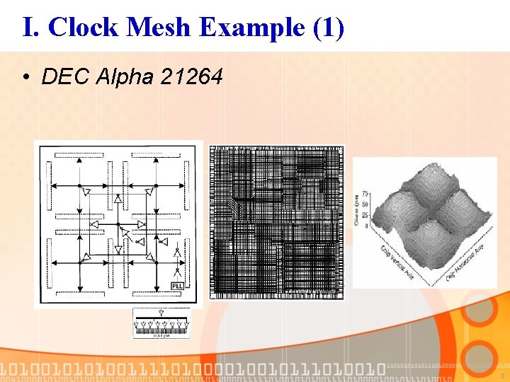
I. Clock Mesh Example (1) • DEC Alpha 21264 3

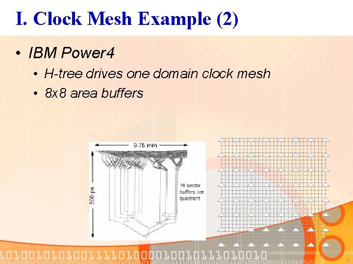
I. Clock Mesh Example (2) • IBM Power 4 • H-tree drives one domain clock mesh • 8 x 8 area buffers 4

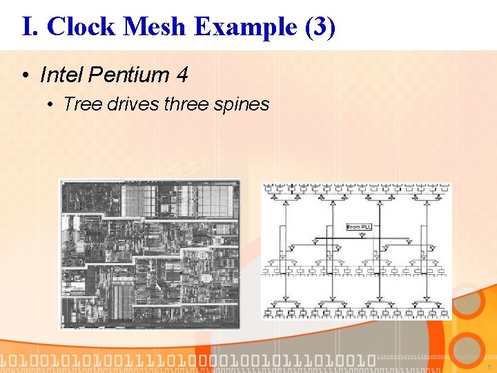
I. Clock Mesh Example (3) • Intel Pentium 4 • Tree drives three spines 5

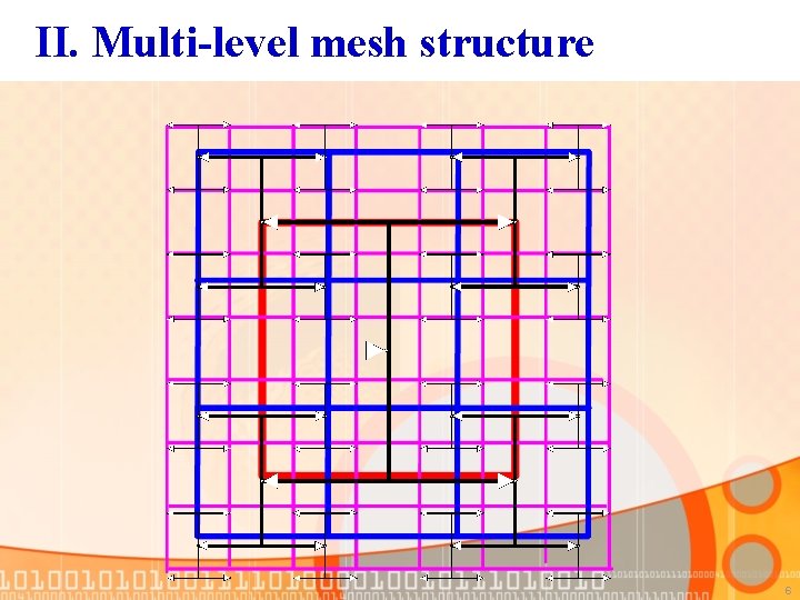
II. Multi-level mesh structure 6

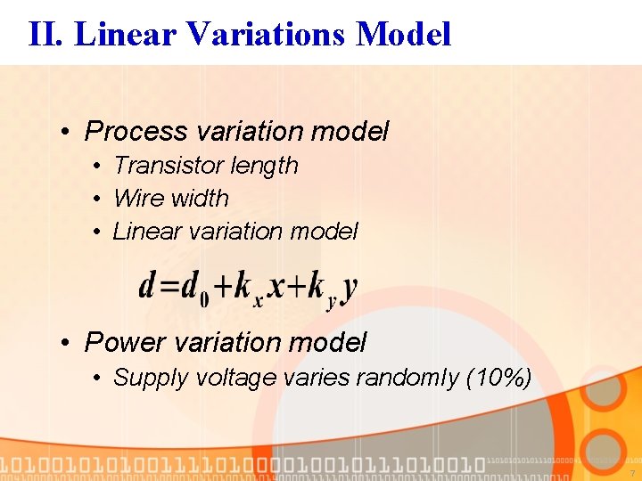
II. Linear Variations Model • Process variation model • Transistor length • Wire width • Linear variation model • Power variation model • Supply voltage varies randomly (10%) 7

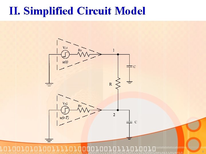
II. Simplified Circuit Model 8

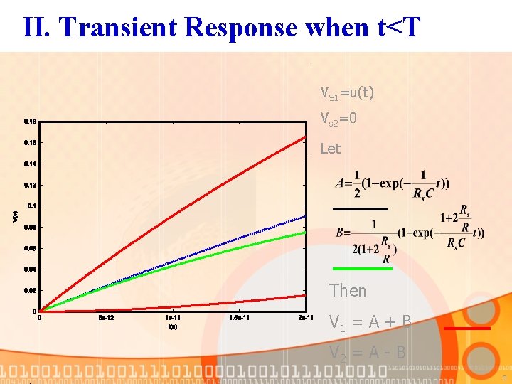
II. Transient Response when t<T VS 1=u(t) Vs 2=0 Let Then V 1 = A + B V 2 = A - B 9

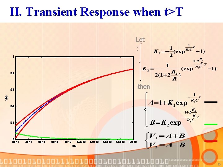
II. Transient Response when t>T Let : then 10

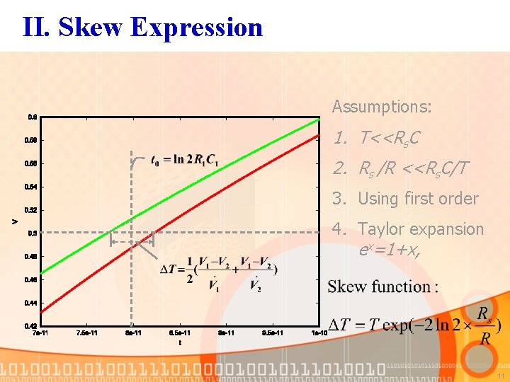
II. Skew Expression Assumptions: 1. T<<Rs. C 2. Rs /R <<Rs. C/T 3. Using first order 4. Taylor expansion ex=1+x, 11

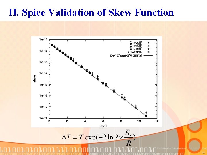
II. Spice Validation of Skew Function 12

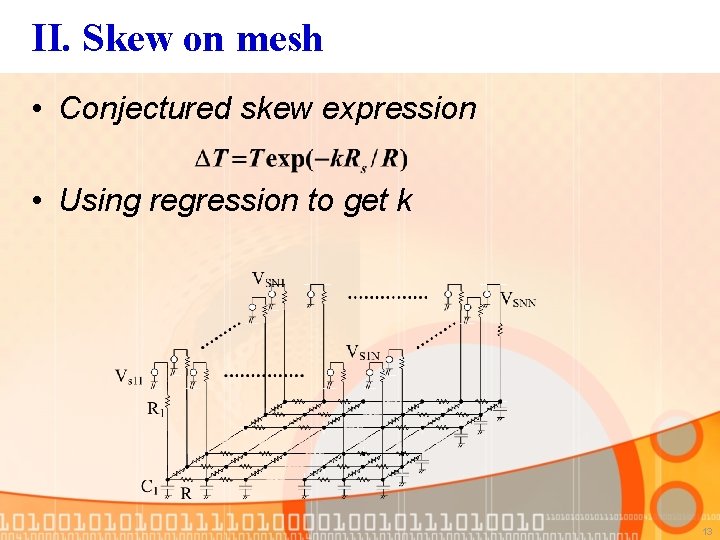
II. Skew on mesh • Conjectured skew expression • Using regression to get k 13

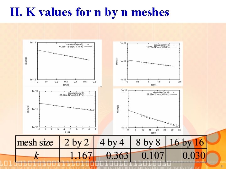
II. K values for n by n meshes 14

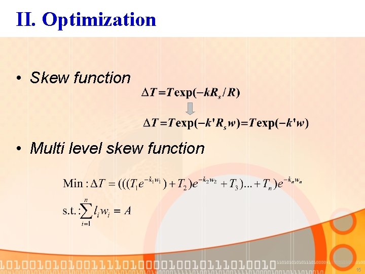
II. Optimization • Skew function • Multi level skew function 15

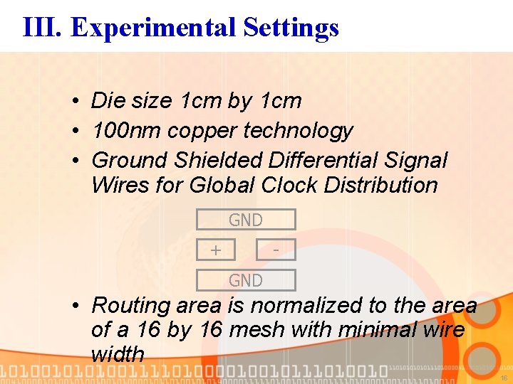
III. Experimental Settings • Die size 1 cm by 1 cm • 100 nm copper technology • Ground Shielded Differential Signal Wires for Global Clock Distribution GND + GND • Routing area is normalized to the area of a 16 by 16 mesh with minimal wire width 16

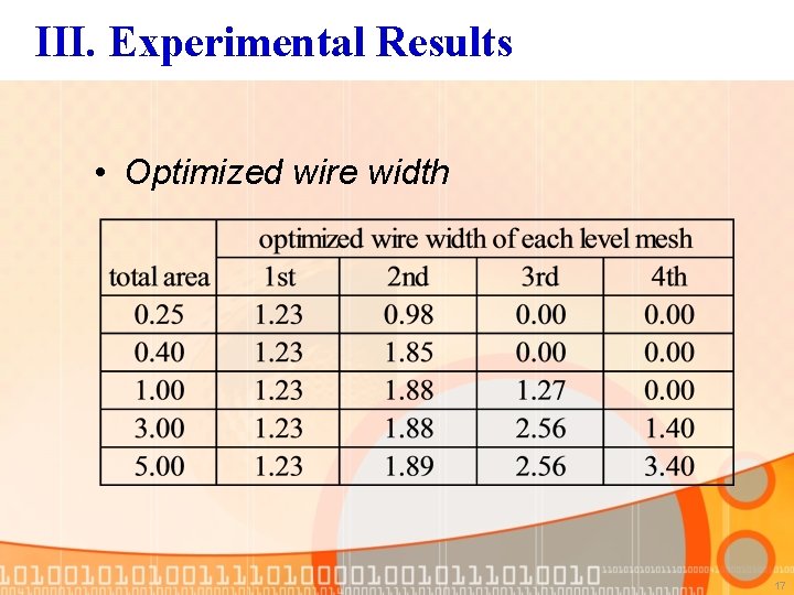
III. Experimental Results • Optimized wire width 17

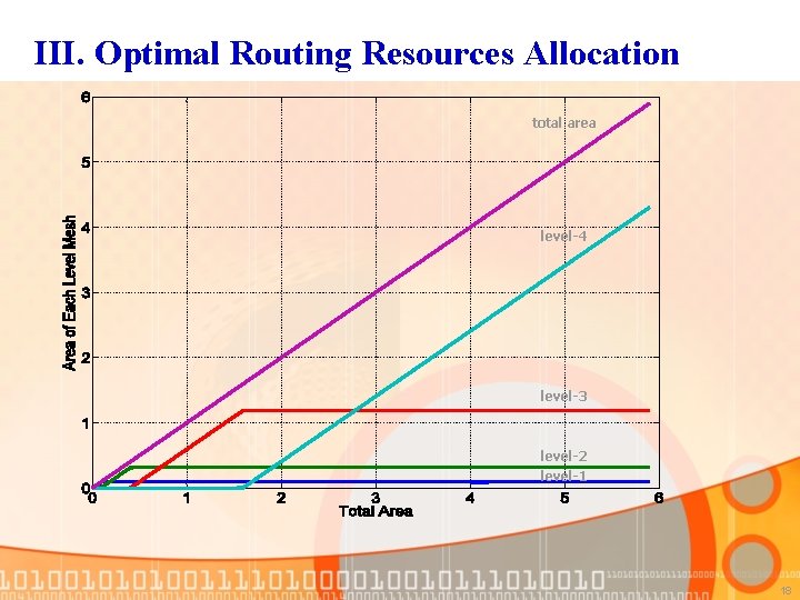
III. Optimal Routing Resources Allocation total area level-4 level-3 level-2 level-1 18

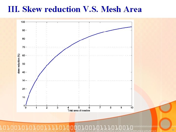
III. Skew reduction V. S. Mesh Area 19

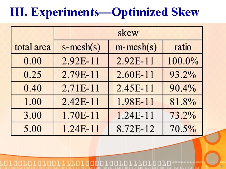
III. Experiments—Optimized Skew 20

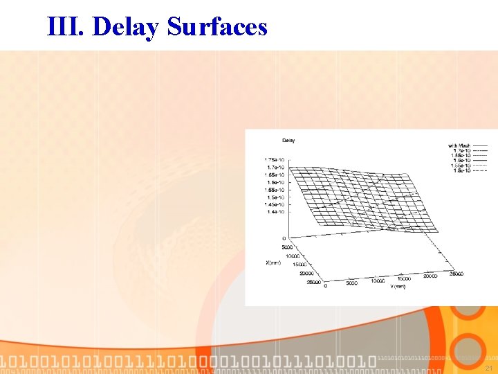
III. Delay Surfaces 21

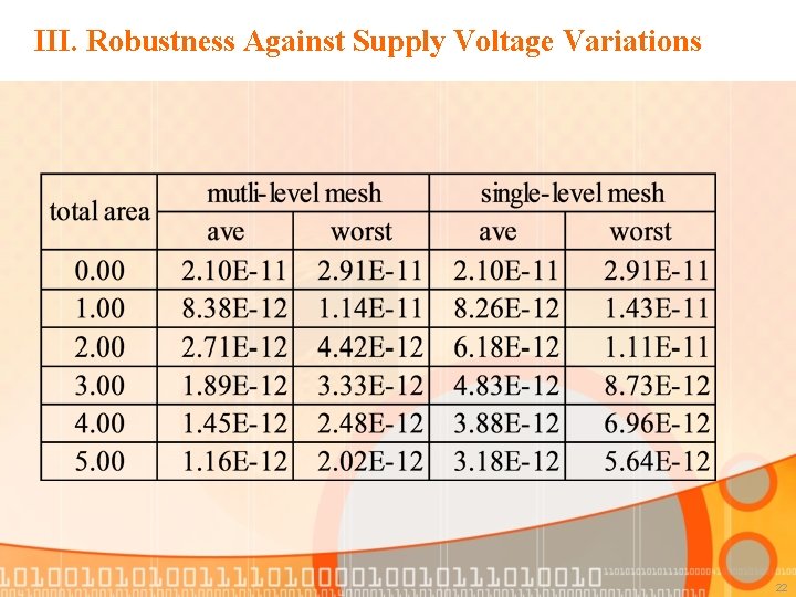
III. Robustness Against Supply Voltage Variations 22

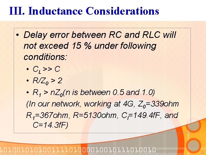
III. Inductance Considerations • Delay error between RC and RLC will not exceed 15 % under following conditions: • CL >> C • R/Z 0 > 2 • R 1 > n. Z 0(n is between 0. 5 and 1. 0) (In our network, working at 4 G, Z 0=339 ohm R 1=367 ohm, R=5130 ohm, Cl=149. 4 f. F, and C=14. 3 f. F) 23

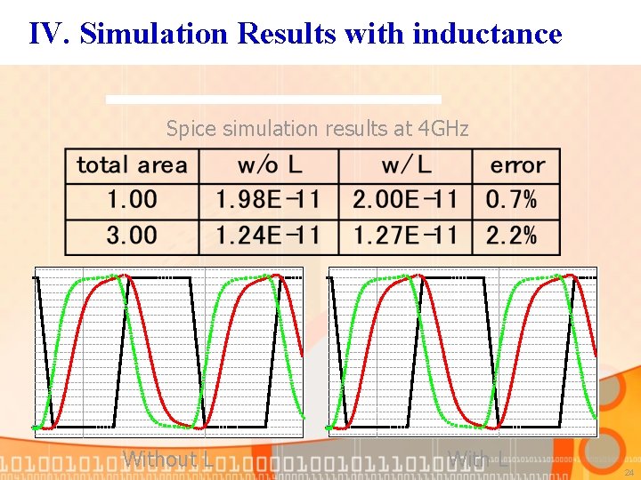
IV. Simulation Results with inductance Spice simulation results at 4 GHz Without L With L 24

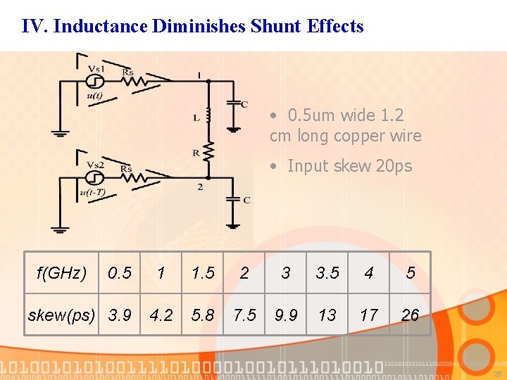
IV. Inductance Diminishes Shunt Effects • 0. 5 um wide 1. 2 cm long copper wire • Input skew 20 ps f(GHz) 0. 5 skew(ps) 3. 9 1 1. 5 2 3 3. 5 4. 2 5. 8 7. 5 9. 9 13 17 26 25