Lecture 19 Packaging Power Clock Outline q Packaging



- Slides: 31

Lecture 19: Packaging, Power, & Clock

Outline q Packaging q Power Distribution q Clock Distribution 21: Package, Power, and Clock CMOS VLSI Design 4 th Ed. 2

Packages q Package functions – Electrical connection of signals and power from chip to board – Little delay or distortion – Mechanical connection of chip to board – Removes heat produced on chip – Protects chip from mechanical damage – Compatible with thermal expansion – Inexpensive to manufacture and test 21: Package, Power, and Clock CMOS VLSI Design 4 th Ed. 3

Package Types q Through-hole vs. surface mount 21: Package, Power, and Clock CMOS VLSI Design 4 th Ed. 4

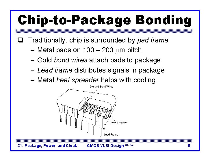
Chip-to-Package Bonding q Traditionally, chip is surrounded by pad frame – Metal pads on 100 – 200 mm pitch – Gold bond wires attach pads to package – Lead frame distributes signals in package – Metal heat spreader helps with cooling 21: Package, Power, and Clock CMOS VLSI Design 4 th Ed. 5

Advanced Packages q Bond wires contribute parasitic inductance q Fancy packages have many signal, power layers – Like tiny printed circuit boards q Flip-chip places connections across surface of die rather than around periphery – Top level metal pads covered with solder balls – Chip flips upside down – Carefully aligned to package (done blind!) – Heated to melt balls – Also called C 4 (Controlled Collapse Chip Connection) 21: Package, Power, and Clock CMOS VLSI Design 4 th Ed. 6

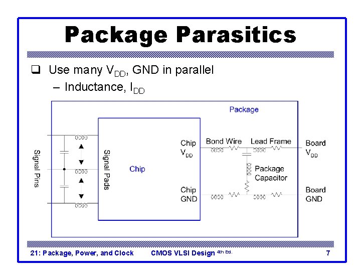
Package Parasitics q Use many VDD, GND in parallel – Inductance, IDD 21: Package, Power, and Clock CMOS VLSI Design 4 th Ed. 7

Heat Dissipation q 60 W light bulb has surface area of 120 cm 2 q Itanium 2 die dissipates 130 W over 4 cm 2 – Chips have enormous power densities – Cooling is a serious challenge q Package spreads heat to larger surface area – Heat sinks may increase surface area further – Fans increase airflow rate over surface area – Liquid cooling used in extreme cases ($$$) 21: Package, Power, and Clock CMOS VLSI Design 4 th Ed. 8

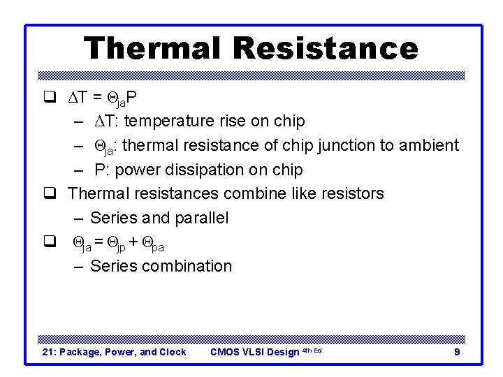
Thermal Resistance q ΔT = Θja. P – ΔT: temperature rise on chip – Θja: thermal resistance of chip junction to ambient – P: power dissipation on chip q Thermal resistances combine like resistors – Series and parallel q Θja = Θjp + Θpa – Series combination 21: Package, Power, and Clock CMOS VLSI Design 4 th Ed. 9

Example q Your chip has a heat sink with a thermal resistance to the package of 4. 0° C/W. q The resistance from chip to package is 1° C/W. q The system box ambient temperature may reach 55° C. q The chip temperature must not exceed 100° C. q What is the maximum chip power dissipation? q (100 -55 C) / (4 + 1 C/W) = 9 W 21: Package, Power, and Clock CMOS VLSI Design 4 th Ed. 10

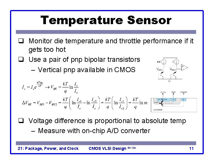
Temperature Sensor q Monitor die temperature and throttle performance if it gets too hot q Use a pair of pnp bipolar transistors – Vertical pnp available in CMOS q Voltage difference is proportional to absolute temp – Measure with on-chip A/D converter 21: Package, Power, and Clock CMOS VLSI Design 4 th Ed. 11

Power Distribution q Power Distribution Network functions – Carry current from pads to transistors on chip – Maintain stable voltage with low noise – Provide average and peak power demands – Provide current return paths for signals – Avoid electromigration & self-heating wearout – Consume little chip area and wire – Easy to lay out 21: Package, Power, and Clock CMOS VLSI Design 4 th Ed. 12

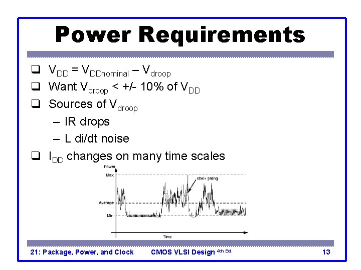
Power Requirements q VDD = VDDnominal – Vdroop q Want Vdroop < +/- 10% of VDD q Sources of Vdroop – IR drops – L di/dt noise q IDD changes on many time scales 21: Package, Power, and Clock CMOS VLSI Design 4 th Ed. 13

IR Drop q A chip draws 24 W from a 1. 2 V supply. The power supply impedance is 5 mΩ. What is the IR drop? q IDD = 24 W / 1. 2 V = 20 A q IR drop = (20 A)(5 mΩ) = 100 m. V 21: Package, Power, and Clock CMOS VLSI Design 4 th Ed. 14

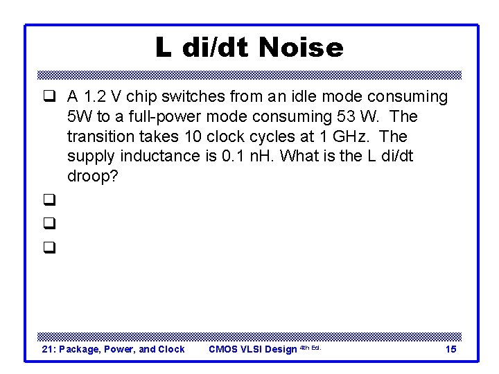
L di/dt Noise q A 1. 2 V chip switches from an idle mode consuming 5 W to a full-power mode consuming 53 W. The transition takes 10 clock cycles at 1 GHz. The supply inductance is 0. 1 n. H. What is the L di/dt droop? q ΔI = (53 W – 5 W)/(1. 2 V) = 40 A q Δt = 10 cycles * (1 ns / cycle) = 10 ns q L di/dt droop = (0. 1 n. H) * (40 A / 10 ns) = 0. 4 V 21: Package, Power, and Clock CMOS VLSI Design 4 th Ed. 15

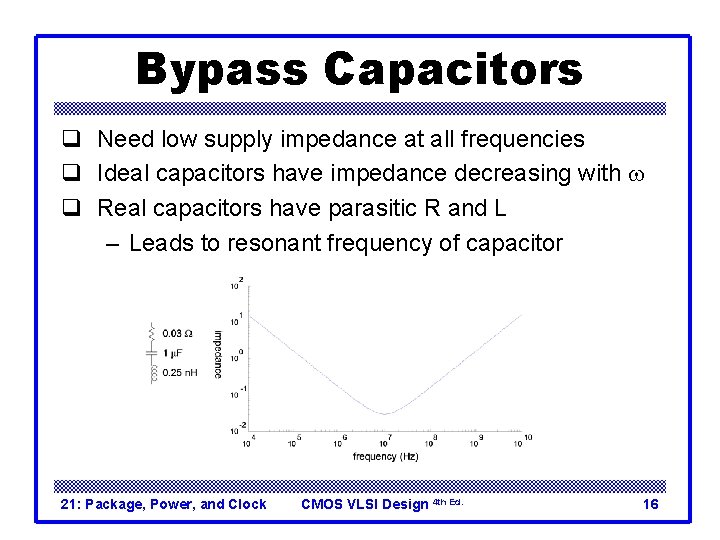
Bypass Capacitors q Need low supply impedance at all frequencies q Ideal capacitors have impedance decreasing with w q Real capacitors have parasitic R and L – Leads to resonant frequency of capacitor 21: Package, Power, and Clock CMOS VLSI Design 4 th Ed. 16

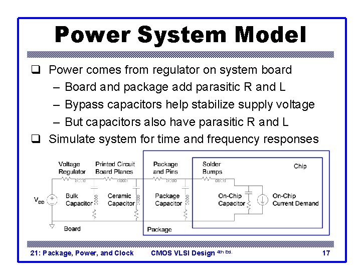
Power System Model q Power comes from regulator on system board – Board and package add parasitic R and L – Bypass capacitors help stabilize supply voltage – But capacitors also have parasitic R and L q Simulate system for time and frequency responses 21: Package, Power, and Clock CMOS VLSI Design 4 th Ed. 17

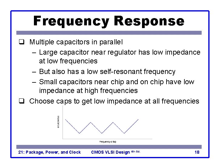
Frequency Response q Multiple capacitors in parallel – Large capacitor near regulator has low impedance at low frequencies – But also has a low self-resonant frequency – Small capacitors near chip and on chip have low impedance at high frequencies q Choose caps to get low impedance at all frequencies 21: Package, Power, and Clock CMOS VLSI Design 4 th Ed. 18

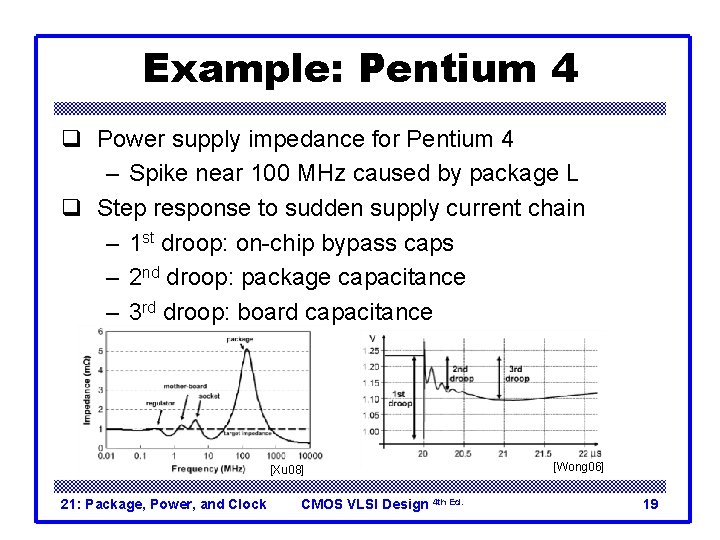
Example: Pentium 4 q Power supply impedance for Pentium 4 – Spike near 100 MHz caused by package L q Step response to sudden supply current chain – 1 st droop: on-chip bypass caps – 2 nd droop: package capacitance – 3 rd droop: board capacitance [Xu 08] 21: Package, Power, and Clock CMOS VLSI Design 4 th Ed. [Wong 06] 19

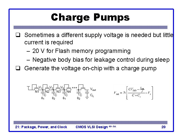
Charge Pumps q Sometimes a different supply voltage is needed but little current is required – 20 V for Flash memory programming – Negative body bias for leakage control during sleep q Generate the voltage on-chip with a charge pump 21: Package, Power, and Clock CMOS VLSI Design 4 th Ed. 20

Energy Scavenging q Ultra-low power systems can scavenge their energy from the environment rather than needing batteries – Solar calculator (solar cells) – RFID tags (antenna) – Tire pressure monitors powered by vibrational energy of tires (piezoelectric generator) q Thin film microbatteries deposited on the chip can store energy for times of peak demand 21: Package, Power, and Clock CMOS VLSI Design 4 th Ed. 21

Clock Distribution q On a small chip, the clock distribution network is just a wire – And possibly an inverter for clkb q On practical chips, the RC delay of the wire resistance and gate load is very long – Variations in this delay cause clock to get to different elements at different times – This is called clock skew q Most chips use repeaters to buffer the clock and equalize the delay – Reduces but doesn’t eliminate skew 21: Package, Power, and Clock CMOS VLSI Design 4 th Ed. 22

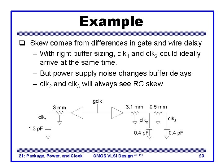
Example q Skew comes from differences in gate and wire delay – With right buffer sizing, clk 1 and clk 2 could ideally arrive at the same time. – But power supply noise changes buffer delays – clk 2 and clk 3 will always see RC skew 21: Package, Power, and Clock CMOS VLSI Design 4 th Ed. 23

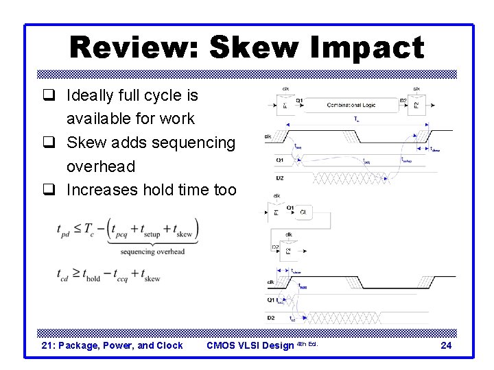
Review: Skew Impact q Ideally full cycle is available for work q Skew adds sequencing overhead q Increases hold time too 21: Package, Power, and Clock CMOS VLSI Design 4 th Ed. 24

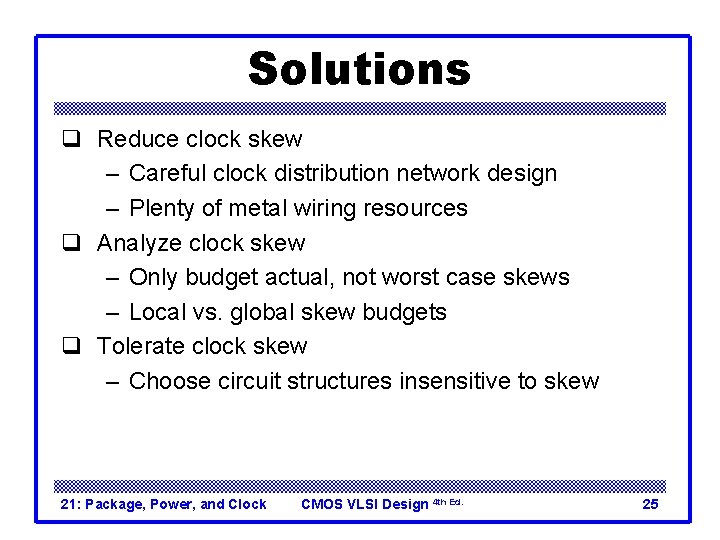
Solutions q Reduce clock skew – Careful clock distribution network design – Plenty of metal wiring resources q Analyze clock skew – Only budget actual, not worst case skews – Local vs. global skew budgets q Tolerate clock skew – Choose circuit structures insensitive to skew 21: Package, Power, and Clock CMOS VLSI Design 4 th Ed. 25

Clock Dist. Networks q q Ad hoc Grids H-tree Hybrid 21: Package, Power, and Clock CMOS VLSI Design 4 th Ed. 26

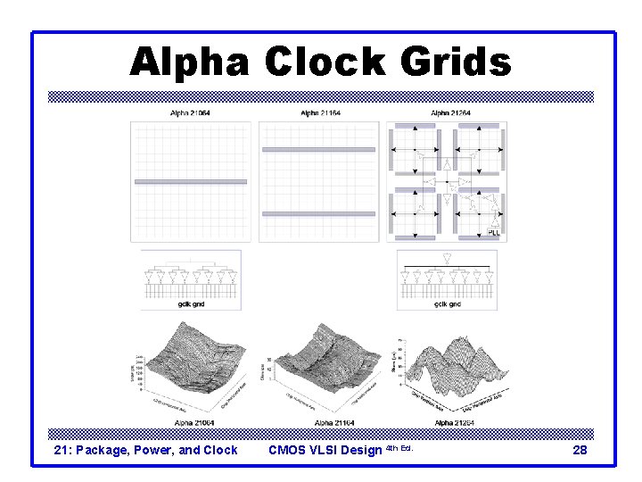
Clock Grids q q Use grid on two or more levels to carry clock Make wires wide to reduce RC delay Ensures low skew between nearby points But possibly large skew across die 21: Package, Power, and Clock CMOS VLSI Design 4 th Ed. 27

Alpha Clock Grids 21: Package, Power, and Clock CMOS VLSI Design 4 th Ed. 28

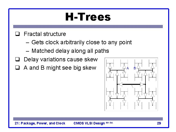
H-Trees q Fractal structure – Gets clock arbitrarily close to any point – Matched delay along all paths q Delay variations cause skew q A and B might see big skew 21: Package, Power, and Clock CMOS VLSI Design 4 th Ed. 29

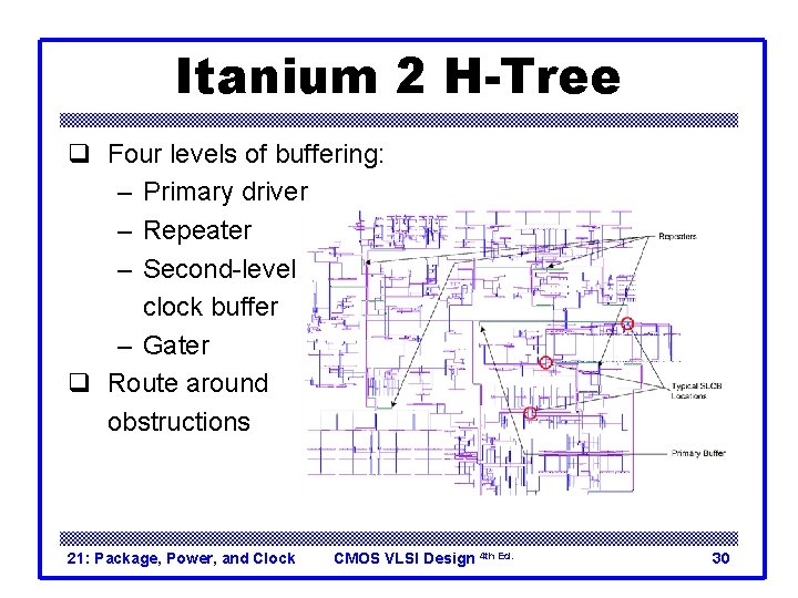
Itanium 2 H-Tree q Four levels of buffering: – Primary driver – Repeater – Second-level clock buffer – Gater q Route around obstructions 21: Package, Power, and Clock CMOS VLSI Design 4 th Ed. 30

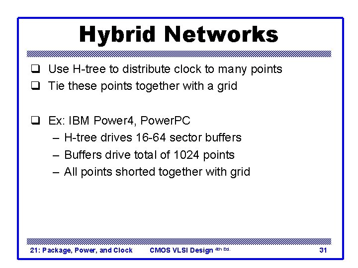
Hybrid Networks q Use H-tree to distribute clock to many points q Tie these points together with a grid q Ex: IBM Power 4, Power. PC – H-tree drives 16 -64 sector buffers – Buffers drive total of 1024 points – All points shorted together with grid 21: Package, Power, and Clock CMOS VLSI Design 4 th Ed. 31