IIVI Semiconductor Materials Devices and Applications Lorelei Lewandowski


- Slides: 22

II-VI Semiconductor Materials, Devices, and Applications Lorelei Lewandowski 4/20/2015 There are 7 II-VI semiconductor materials. Because of their direct, wide band gap energy, they are becoming increasingly useful in optical applications. While some of them have been around for many years, research is still needed to determine the full potential of others. The “latest and greatest” technology in the near future will most likely owe much of its success to these materials.

OUTLINE/INTRO ØList of II-VI Semiconductor Materials ØGeneral Common Properties ØCommon Usage of Each ØOverview/Conclusion ØReferences ØConcept Check

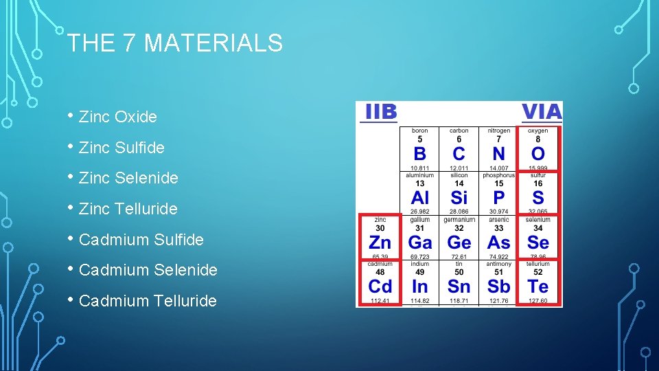
THE 7 MATERIALS • Zinc Oxide • Zinc Sulfide • Zinc Selenide • Zinc Telluride • Cadmium Sulfide • Cadmium Selenide • Cadmium Telluride

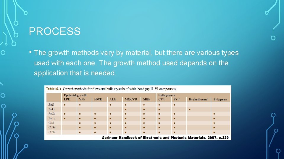
PROCESS • The growth methods vary by material, but there are various types used with each one. The growth method used depends on the application that is needed.

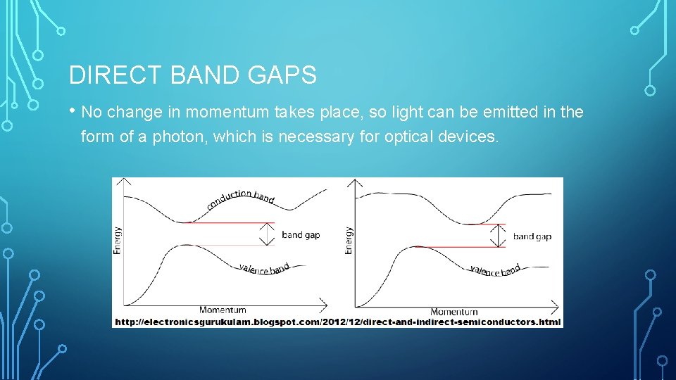
DIRECT BAND GAPS • No change in momentum takes place, so light can be emitted in the form of a photon, which is necessary for optical devices.

WIDE BAND GAP • These 7 materials have band gaps ranging from 1. 5 e. V to 3. 54 e. V. • Perspective: Si has a band gap of 1. 1 e. V and Ga. As 1. 4 e. V. • A wider band gap is one property that these materials have in common. Because of this, they have various common applications such as: • • LEDs & LDs Signal Processing

ADVANTAGES • Higher Iconicity & Stronger Bonds = Higher Melting Temp • Less Energy Lost = More Efficient & Potential For Lower Cost • Higher Breakdown Voltage = High Power & Freq Applications • Higher Doping Concentration = Thinner Device Layers • Higher Electron Mobility = Faster Operation

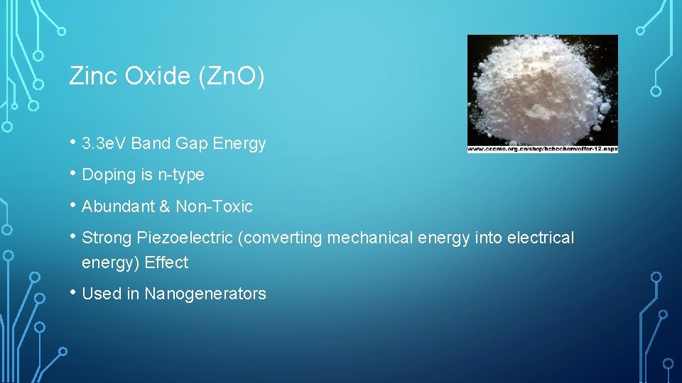
Zinc Oxide (Zn. O) • 3. 3 e. V Band Gap Energy • Doping is n-type • Abundant & Non-Toxic • Strong Piezoelectric (converting mechanical energy into electrical energy) Effect • Used in Nanogenerators

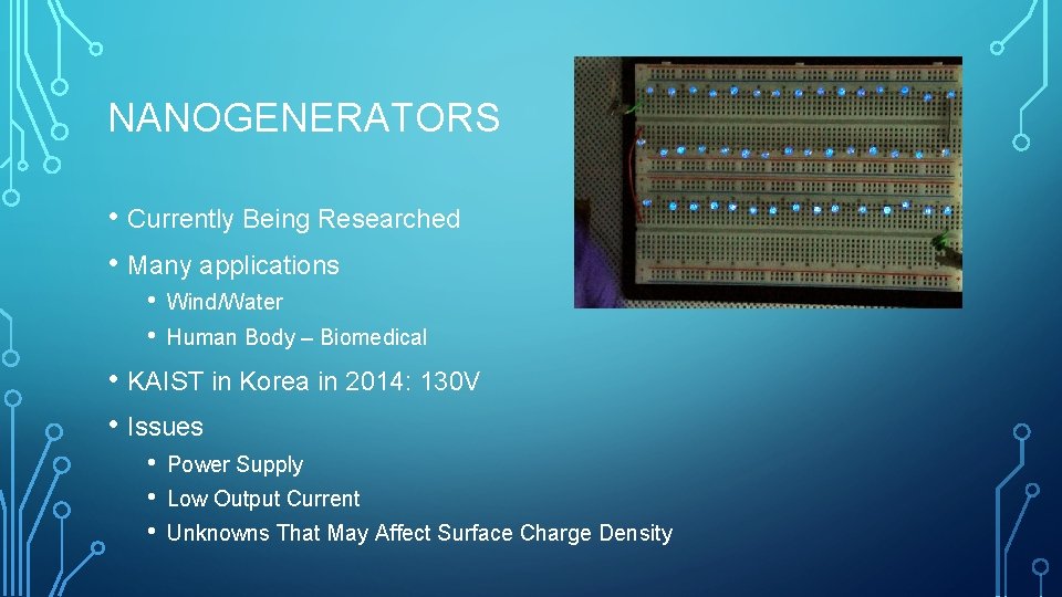
NANOGENERATORS • Currently Being Researched • Many applications • • Wind/Water Human Body – Biomedical • KAIST in Korea in 2014: 130 V • Issues • • • Power Supply Low Output Current Unknowns That May Affect Surface Charge Density

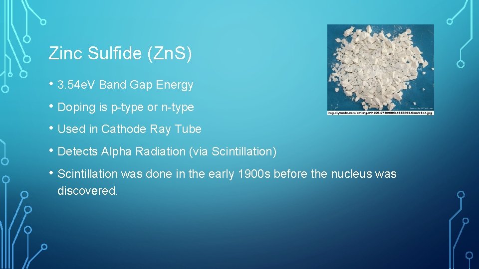
Zinc Sulfide (Zn. S) • 3. 54 e. V Band Gap Energy • Doping is p-type or n-type • Used in Cathode Ray Tube • Detects Alpha Radiation (via Scintillation) • Scintillation was done in the early 1900 s before the nucleus was discovered.

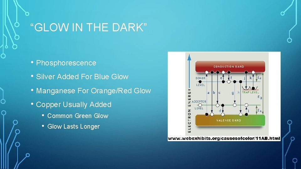
“GLOW IN THE DARK” • Phosphorescence • Silver Added For Blue Glow • Manganese For Orange/Red Glow • Copper Usually Added • • Common Green Glow Lasts Longer

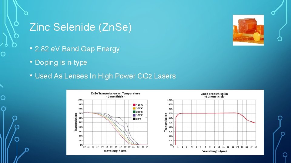
Zinc Selenide (Zn. Se) • 2. 82 e. V Band Gap Energy • Doping is n-type • Used As Lenses In High Power CO 2 Lasers

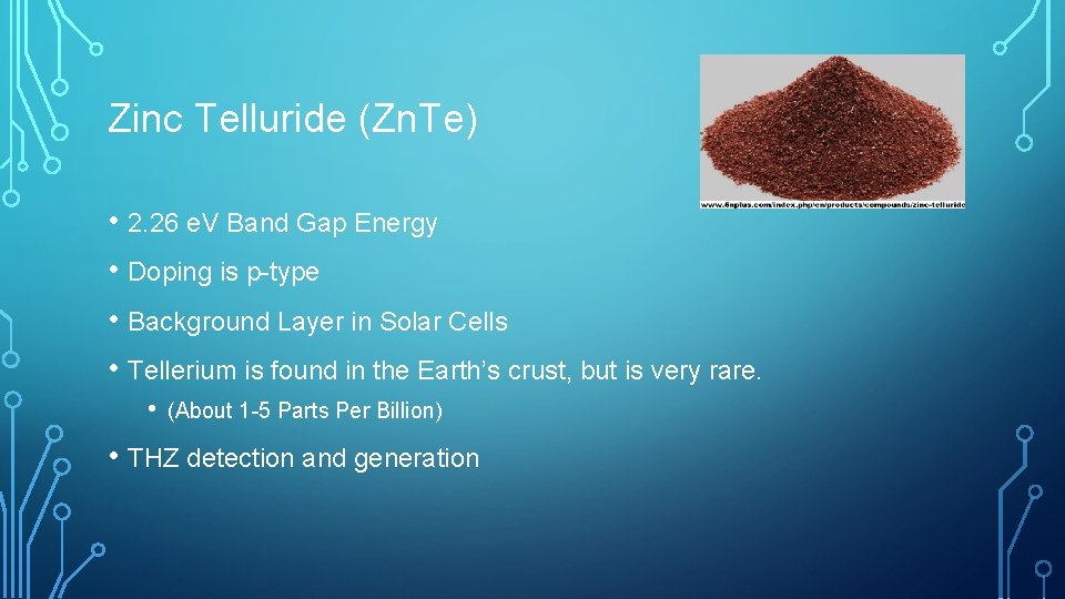
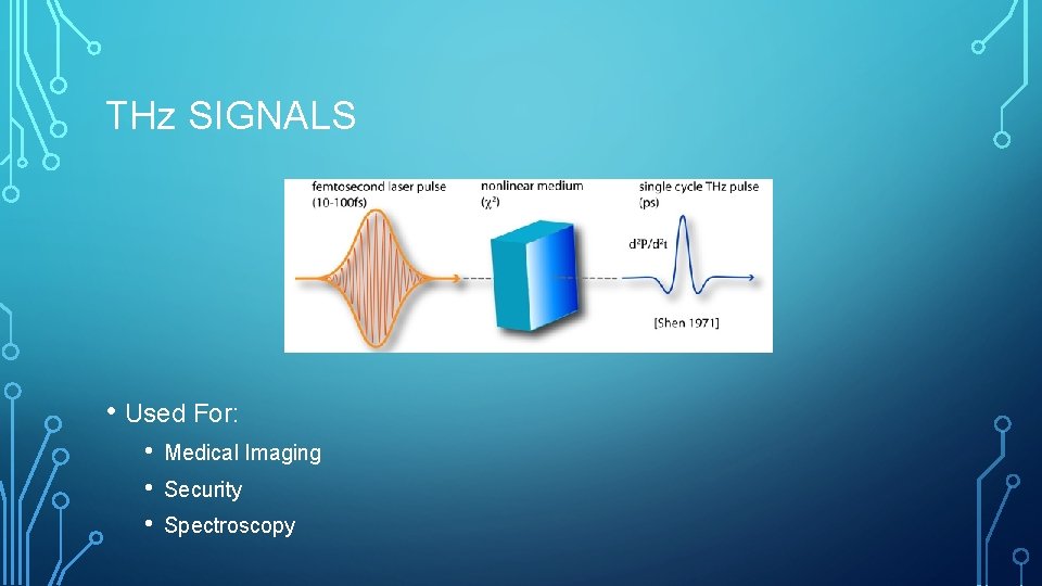
Zinc Telluride (Zn. Te) • 2. 26 e. V Band Gap Energy • Doping is p-type • Background Layer in Solar Cells • Tellerium is found in the Earth’s crust, but is very rare. • (About 1 -5 Parts Per Billion) • THZ detection and generation

THz SIGNALS • Used For: • • • Medical Imaging Security Spectroscopy

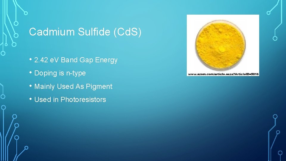
Cadmium Sulfide (Cd. S) • 2. 42 e. V Band Gap Energy • Doping is n-type • Mainly Used As Pigment • Used in Photoresistors

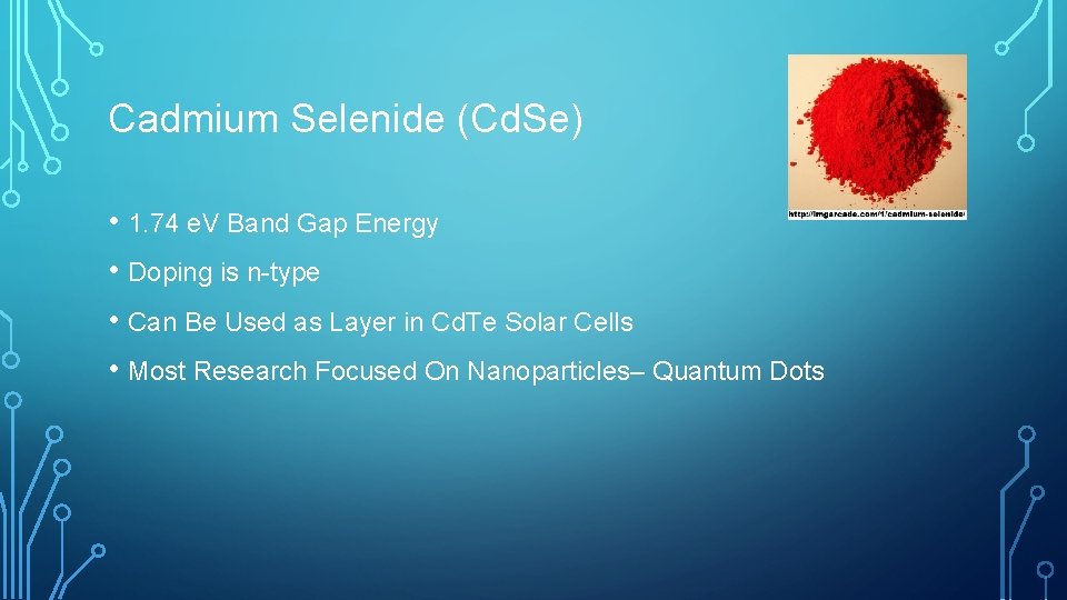
Cadmium Selenide (Cd. Se) • 1. 74 e. V Band Gap Energy • Doping is n-type • Can Be Used as Layer in Cd. Te Solar Cells • Most Research Focused On Nanoparticles– Quantum Dots

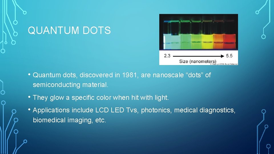
QUANTUM DOTS • Quantum dots, discovered in 1981, are nanoscale “dots” of semiconducting material. • They glow a specific color when hit with light. • Applications include LCD LED Tvs, photonics, medical diagnostics, biomedical imaging, etc.

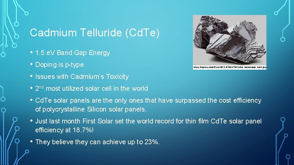
Cadmium Telluride (Cd. Te) • 1. 5 e. V Band Gap Energy • Doping is p-type • Issues with Cadmium’s Toxicity • 2 nd most utilized solar cell in the world • Cd. Te solar panels are the only ones that have surpassed the cost efficiency of polycrystalline Silicon solar panels. • Just last month First Solar set the world record for thin film Cd. Te solar panel efficiency at 18. 7%! • They believe they can achieve up to 23%.

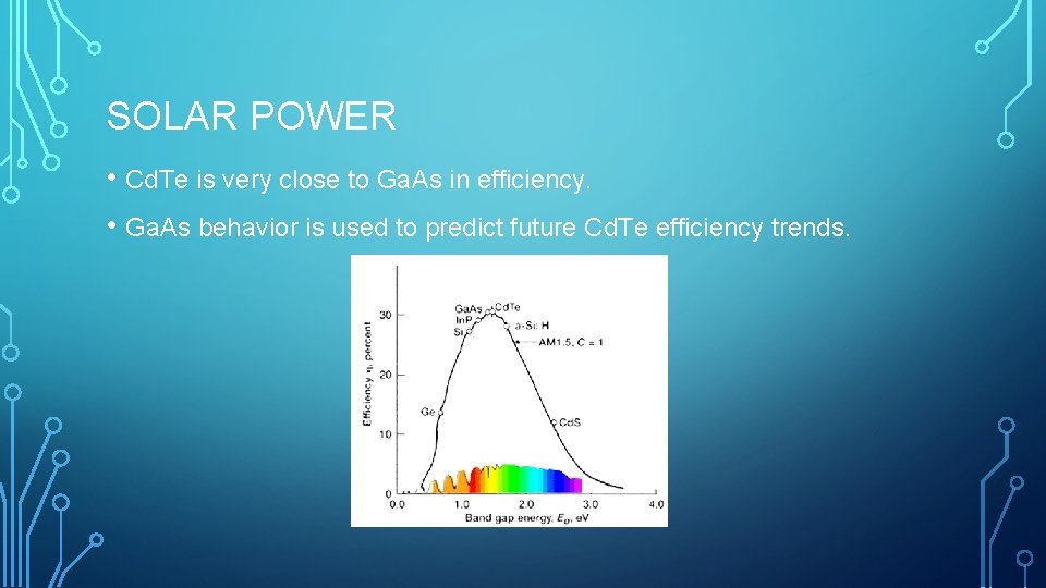
SOLAR POWER • Cd. Te is very close to Ga. As in efficiency. • Ga. As behavior is used to predict future Cd. Te efficiency trends.

SUMMARY & CONCLUSION II-VI semiconductor materials are becoming increasingly important in the semiconductor industry. Nanogenerators have the potential to change the future of electronics while quantum dots and solar panels are integrating themselves into modern electronics. While it’s impossible to determine just how large of an effect these materials will have and how long-lived they will be, high power electronics and the medical industry are already benefiting from them.

REFERENCES Ø Ø Academic Sources (Articles, Textbooks, IEEE Spectrum) Ø Ø http: //psec. uchicago. edu/library/microchannel_plates/zinc_oxide. pdf Ø Ø Ø http: //scholar. lib. vt. edu/theses/available/etd-04262005 -181042/unrestricted/Ch 1 Applications. pdf https: //books. google. com/books? id=q. Cebx. Pjd. SBUC&pg=PA 110&lpg=PA 110&dq=radioactive+decay+zns&source=bl&ots=H 2 Ni. CPCG 8 P&sig=4 Jy. Dvte. Nb. Bw. ENa. QYiov. Vmp. Jl 0 s&hl=en&sa=X&ei=3 r. Qw. Vfy. PJ 4 y. Zs. AWdk. YC 4 Dw&ved=0 CCYQ 6 AEw. Ag#v=onepage&q&f=false http: //link. springer. com/article/10. 1007%2 Fs 00216 -007 -1661 -9#page-1 http: //spectrum. ieee. org/tech-talk/semiconductors/nanotechnology/energy-harvesting-nanogenerators-give-130 -volts-at-the-touch-of-a-finger Websites Ø Ø http: //www. azom. com/article. aspx? Article. ID=8415#5 http: //www. firstsolar. com http: //mpsd-cmd. cfel. de/research-met-thz-optrect. html http: //www. iiviinfrared. com/Optical-Materials/znse. html

KEY CONCEPTS 1) Wide/Direct Band Gap – Importance in Photonics 2) What are nanogenerators? 3) What causes things to “glow in the dark”? 4) Quantum Dots Applications 5) Solar Panel Innovation by Cd. Te