Full size pixel chip for highrate CEPC Vertex

- Slides: 22

Full size pixel chip for high-rate CEPC Vertex Detector Wei On behalf of the CEPC MOST 2 Vertex detector design team 2019 -4 -3

Outline • Motivation of the MOST 2 Vertex detector design • Specification • Limitation of the existing CMOS sensors towards the highrate CEPC Vertex Detector • Key improvement for fast readout • Preliminary design & schedule 2

CEPC Vertex Detector Design • Ref: Status of vertex detector, Q. Ouyang, International workshop on CEPC, Nov. 7 th 2017 3

Baseline Vertex Detector design • Ref: Introduction to the Pixel MOST 2 Project, Joao Costa, 2018. 6 4

Ladder Prototype • Ref: Introduction to the Pixel MOST 2 Project, Joao Costa, 2018. 6 5

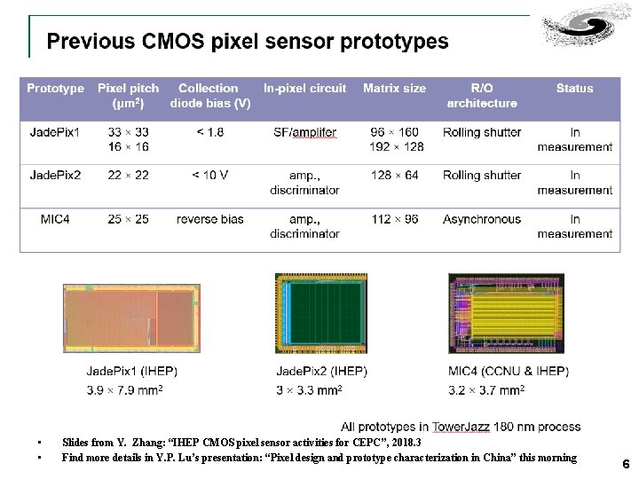
• • Slides from Y. Zhang: “IHEP CMOS pixel sensor activities for CEPC”, 2018. 3 Find more details in Y. P. Lu’s presentation: “Pixel design and prototype characterization in China” this morning 6

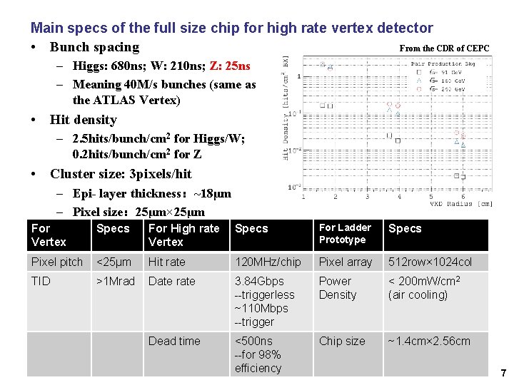
Main specs of the full size chip for high rate vertex detector From the CDR of CEPC • Bunch spacing – Higgs: 680 ns; W: 210 ns; Z: 25 ns – Meaning 40 M/s bunches (same as the ATLAS Vertex) • Hit density – 2. 5 hits/bunch/cm 2 for Higgs/W; 0. 2 hits/bunch/cm 2 for Z • Cluster size: 3 pixels/hit – Epi- layer thickness:~18μm – Pixel size: 25μm× 25μm For Vertex Specs For High rate Vertex Specs For Ladder Prototype Specs Pixel pitch <25μm Hit rate 120 MHz/chip Pixel array 512 row× 1024 col TID >1 Mrad Date rate 3. 84 Gbps --triggerless ~110 Mbps --trigger Power Density < 200 m. W/cm 2 (air cooling) Dead time <500 ns --for 98% efficiency Chip size ~1. 4 cm× 2. 56 cm 7

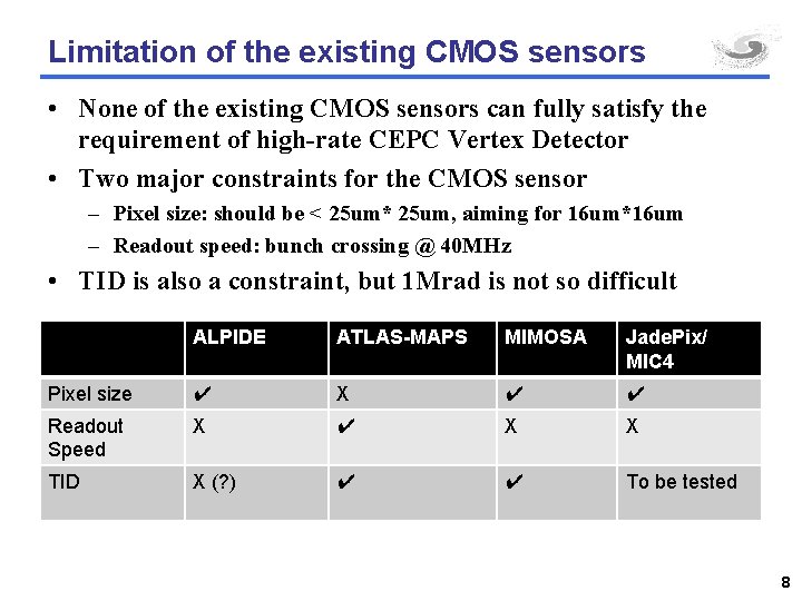
Limitation of the existing CMOS sensors • None of the existing CMOS sensors can fully satisfy the requirement of high-rate CEPC Vertex Detector • Two major constraints for the CMOS sensor – Pixel size: should be < 25 um* 25 um, aiming for 16 um*16 um – Readout speed: bunch crossing @ 40 MHz • TID is also a constraint, but 1 Mrad is not so difficult ALPIDE ATLAS-MAPS MIMOSA Jade. Pix/ MIC 4 Pixel size ✔ X ✔ ✔ Readout Speed X ✔ X X TID X (? ) ✔ ✔ To be tested 8

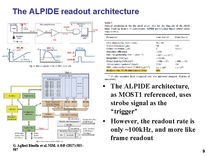
The ALPIDE readout architecture • The ALPIDE architecture, as MOST 1 referenced, uses strobe signal as the “trigger” • However, the readout rate is only ~100 k. Hz, and more like frame readout G. Aglieri Rinella et al. NIM. A 845 (2017) 583– 587 9

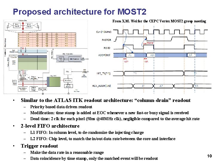
Proposed architecture for MOST 2 From X. M. Wei for the CEPC Vertex MOST 2 group meeting • Similar to the ATLAS ITK readout architecture: “column-drain” readout – – – • 2 -level FIFO architecture – – • Priority based data driven readout Modification: time stamp is added at EOC whenever a new fast-or busy signal is received Dead time: 2 clk for each pixel (50 ns @40 MHz clk), negligible compared to the average hit rate L 1 FIFO: In column level, to de-randomize the injecting charge L 2 FIFO: Chip level, to match the in/out data rate between the core and interface Trigger readout – – Make the data rate in a reasonable range Data coincidence by time stamp, only the matched event will be readout 10

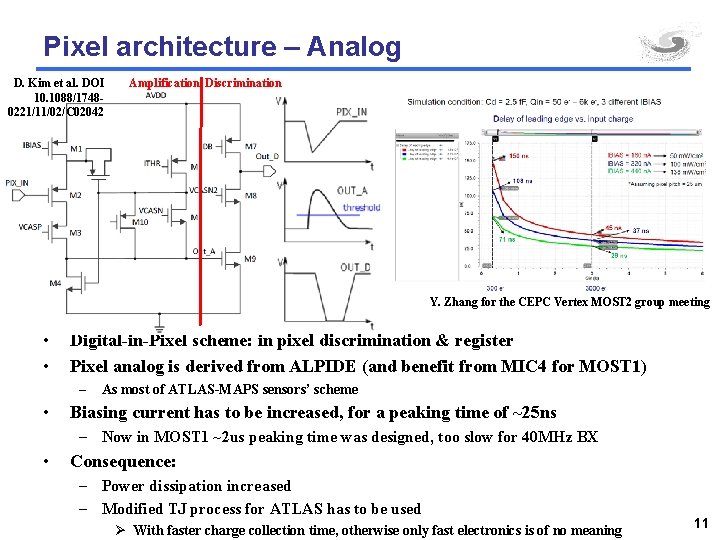
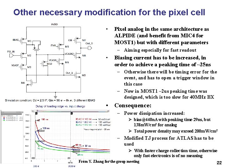
Pixel architecture – Analog D. Kim et al. DOI 10. 1088/17480221/11/02/C 02042 Amplification Discrimination Y. Zhang for the CEPC Vertex MOST 2 group meeting • • Digital-in-Pixel scheme: in pixel discrimination & register Pixel analog is derived from ALPIDE (and benefit from MIC 4 for MOST 1) – • As most of ATLAS-MAPS sensors’ scheme Biasing current has to be increased, for a peaking time of ~25 ns – Now in MOST 1 ~2 us peaking time was designed, too slow for 40 MHz BX • Consequence: – Power dissipation increased – Modified TJ process for ATLAS has to be used Ø With faster charge collection time, otherwise only fast electronics is of no meaning 11

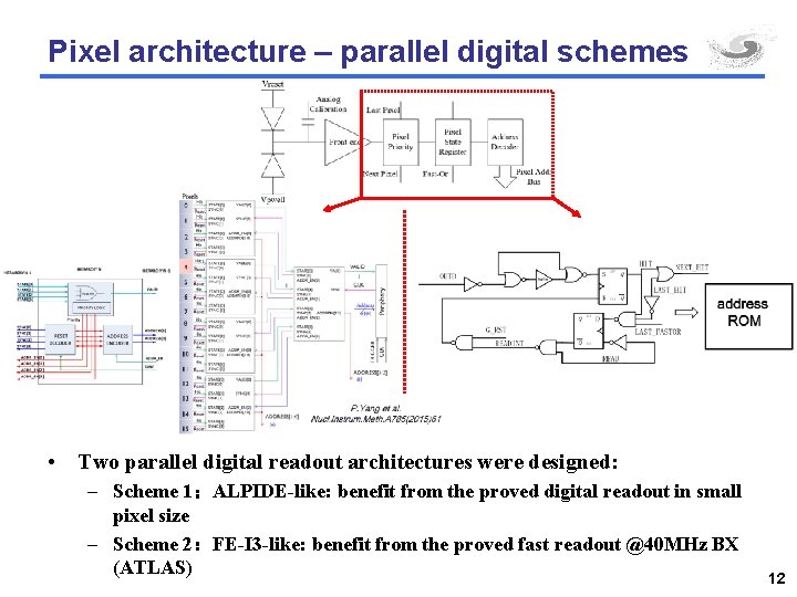
Pixel architecture – parallel digital schemes • Two parallel digital readout architectures were designed: – Scheme 1:ALPIDE-like: benefit from the proved digital readout in small pixel size – Scheme 2:FE-I 3 -like: benefit from the proved fast readout @40 MHz BX (ATLAS) 12

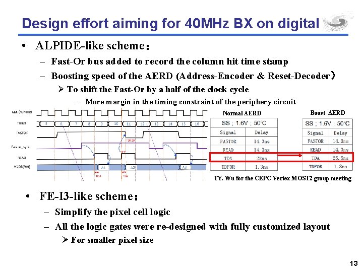
Design effort aiming for 40 MHz BX on digital • ALPIDE-like scheme: – Fast-Or bus added to record the column hit time stamp – Boosting speed of the AERD (Address-Encoder & Reset-Decoder) Ø To shift the Fast-Or by a half of the clock cycle – More margin in the timing constraint of the periphery circuit Normal AERD Boost AERD TY. Wu for the CEPC Vertex MOST 2 group meeting • FE-I 3 -like scheme: – Simplify the pixel cell logic – All the logic gates were re-designed with fully customized layout Ø For smaller pixel size 13

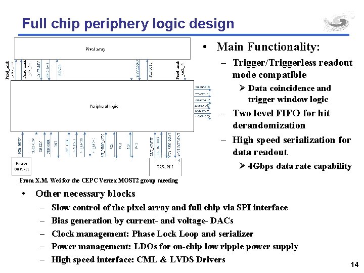
Full chip periphery logic design • Main Functionality: – Trigger/Triggerless readout mode compatible Ø Data coincidence and trigger window logic – Two level FIFO for hit derandomization – High speed serialization for data readout Ø 4 Gbps data rate capability From X. M. Wei for the CEPC Vertex MOST 2 group meeting • Other necessary blocks – – – Slow control of the pixel array and full chip via SPI interface Bias generation by current- and voltage- DACs Clock management: Phase Lock Loop and serializer Power management: LDOs for on-chip low ripple power supply High speed interface: CML & LVDS Drivers 14

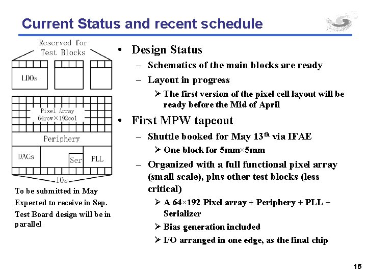
Current Status and recent schedule • Design Status – Schematics of the main blocks are ready – Layout in progress Ø The first version of the pixel cell layout will be ready before the Mid of April • First MPW tapeout – Shuttle booked for May 13 th via IFAE Ø One block for 5 mm× 5 mm To be submitted in May Expected to receive in Sep. Test Board design will be in parallel – Organized with a full functional pixel array (small scale), plus other test blocks (less critical) Ø A 64× 192 Pixel array + Periphery + PLL + Serializer Ø Bias generation included Ø I/O arranged in one edge, as the final chip 15

Summary • MOST 2 Vertex detector sensor design will be benefit from existing MOST 1 designs, with further development on fast readout • Readout architecture modified from “strobed-trigger” readout into “column-drain” readout – Based on priority readout and data driven – Two level FIFOs designed with negligible dead time • Time stamp added for each hit cluster – trigger coincidence will use the time stamp for arbitration • Pixel analog modified for faster peaking time – Aiming for ~25 ns peaking time – Power dissipation increased consequently – modified TJ process is necessary for faster charge collection time • Two parallel pixel digital schemes were designed, based on ALPIDE and FE-I 3, respectively 16

Thank you!

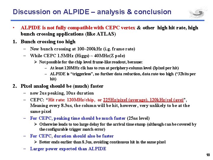
Discussion on ALPIDE – analysis & conclusion • ALPIDE is not fully compatible with CEPC vertex & other high hit rate, high bunch crossing applications (like ATLAS) 1. Bunch crossing too high – Now bunch crossing at 100~200 k. Hz (i. g. frame rate) – While CEPC 1. 5 MHz (Higgs) ~ 40 MHz(Z pole) Ø Not possible for the chip level frame-like readout, because: – At least 120 MHz clk has to run at periphery-column level (3 pixel per hit) – ALPIDE is “triggerless”, no further data reduction, data rate too high (*32 bits per hit) 2. Pixel analog should be (much) faster – now 2 us peaking, 10 us duration – CEPC: “Hit rate: 120 MHz/chip, or 225 Hz/pixel (average), 120 k. Hz/col (ave)”, Meaning every 8. 3 us, the column will be hit, however, very unlikely to be at the same pixel – For CEPC, peaking time should be much faster (25 ns level) Ø Otherwise leads to too large delay for the arrival time stamp (although can be covered by the configurable trigger match error) – For CEPC, duration should also be faster Ø Better ends earlier than 8. 3 us, avoiding continuous hit in the same pixel – Larger power expected than ALPIDE 18

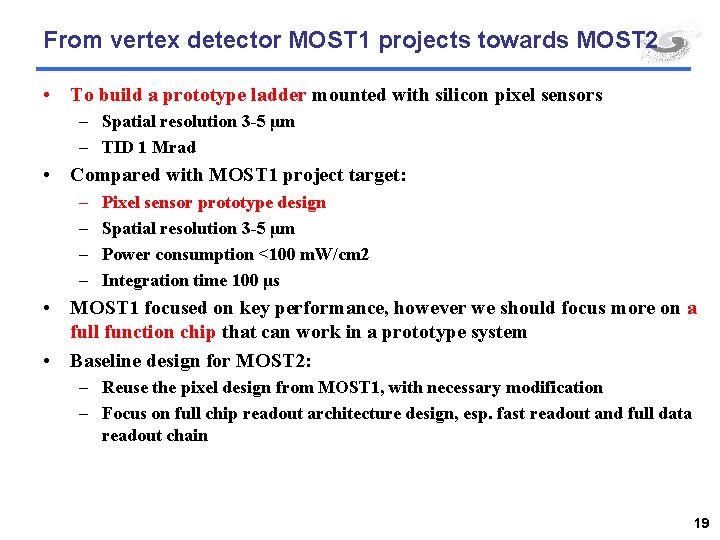
From vertex detector MOST 1 projects towards MOST 2 • To build a prototype ladder mounted with silicon pixel sensors – Spatial resolution 3 -5 μm – TID 1 Mrad • Compared with MOST 1 project target: – – Pixel sensor prototype design Spatial resolution 3 -5 μm Power consumption <100 m. W/cm 2 Integration time 100 μs • MOST 1 focused on key performance, however we should focus more on a full function chip that can work in a prototype system • Baseline design for MOST 2: – Reuse the pixel design from MOST 1, with necessary modification – Focus on full chip readout architecture design, esp. fast readout and full data readout chain 19

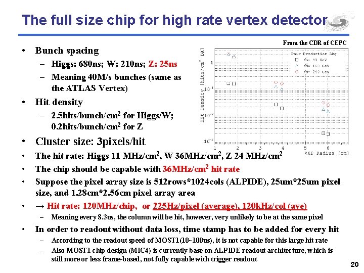
The full size chip for high rate vertex detector • Bunch spacing From the CDR of CEPC – Higgs: 680 ns; W: 210 ns; Z: 25 ns – Meaning 40 M/s bunches (same as the ATLAS Vertex) • Hit density – 2. 5 hits/bunch/cm 2 for Higgs/W; 0. 2 hits/bunch/cm 2 for Z • Cluster size: 3 pixels/hit • • The hit rate: Higgs 11 MHz/cm 2, W 36 MHz/cm 2, Z 24 MHz/cm 2 The chip should be capable with 36 MHz/cm 2 hit rate Suppose the pixel array size is 512 rows*1024 cols (ALPIDE), 25 um*25 um pixel size, and 1. 28 cm*2. 56 cm pixel array area → Hit rate: 120 MHz/chip, or 225 Hz/pixel (average), 120 k. Hz/col (ave) – • Meaning every 8. 3 us, the column will be hit, however, very unlikely to be at the same pixel In order to readout without data loss, time stamp has to be added for every hit – – According to the readout speed of MOST 1(10~100 us), it is not capable for this large hit rate Also MOST 1 chip design (MIC 4) is currently base on ALPIDE readout architecture, which is still more or less frame-based, not fully capable with trigger readout 20

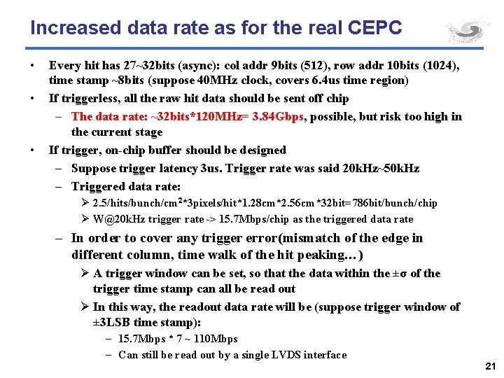
Increased data rate as for the real CEPC • • • Every hit has 27~32 bits (async): col addr 9 bits (512), row addr 10 bits (1024), time stamp ~8 bits (suppose 40 MHz clock, covers 6. 4 us time region) If triggerless, all the raw hit data should be sent off chip – The data rate: ~32 bits*120 MHz= 3. 84 Gbps, possible, but risk too high in the current stage If trigger, on-chip buffer should be designed – Suppose trigger latency 3 us. Trigger rate was said 20 k. Hz~50 k. Hz – Triggered data rate: Ø 2. 5/hits/bunch/cm 2*3 pixels/hit*1. 28 cm*2. 56 cm*32 bit=786 bit/bunch/chip Ø W@20 k. Hz trigger rate -> 15. 7 Mbps/chip as the triggered data rate – In order to cover any trigger error(mismatch of the edge in different column, time walk of the hit peaking…) Ø A trigger window can be set, so that the data within the ±σ of the trigger time stamp can all be read out Ø In this way, the readout data rate will be (suppose trigger window of ± 3 LSB time stamp): – 15. 7 Mbps * 7 ~ 110 Mbps – Can still be read out by a single LVDS interface 21

Other necessary modification for the pixel cell • Pixel analog in the same architecture as ALPIDE (and benefit from MIC 4 for MOST 1) but with different parameters – Aiming especially for fast readout • Biasing current has to be increased, in order to achieve a peaking time of ~25 ns – Otherwise there will be timing error for the event, and has to open a trigger window in this case – Now in MOST 1 ~2 us peaking time was designed, which is too slow for 40 MHz BX • Consequence: – Power dissipation increased: Ø bias@440 n. A with peaking time 29 ns, but 138 m. W/cm 2 for analog Ø Total power density may exceed 200 m. W/cm 2 – Modified TJ process for ATLAS has to be used Ø With faster charge collection time, otherwise only fast electronics is of no meaning From Y. Zhang for the group meeting 22