ET 212 Electronics Semiconductors and Diodes Electrical and
- Slides: 33

ET 212 Electronics Semiconductors and Diodes Electrical and Telecommunication Engineering Technology Professor Jang

Acknowledgement I want to express my gratitude to Prentice Hall giving me the permission to use instructor’s material for developing this module. I would like to thank the Department of Electrical and Telecommunications Engineering Technology of NYCCT for giving me support to commence and complete this module. I hope this module is helpful to enhance our students’ academic performance.

Outline • Semiconductor Physics • The PN junction • Biasing the PN junction • The diode • Trouble Shooting Key Words: Semiconductor, Silicon, PN Junction, Forward Bias, Reverse Bias, Diode ET 212 Electronics – Semiconductors Floyd 2

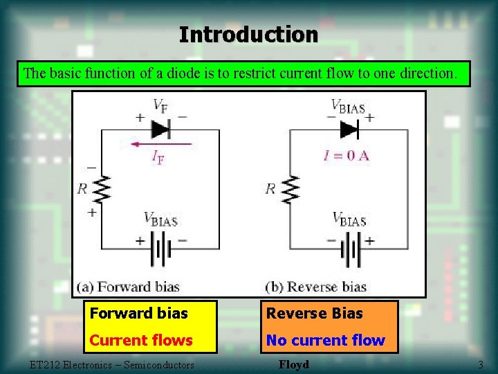
Introduction The basic function of a diode is to restrict current flow to one direction. Forward bias Reverse Bias Current flows No current flow ET 212 Electronics – Semiconductors Floyd 3

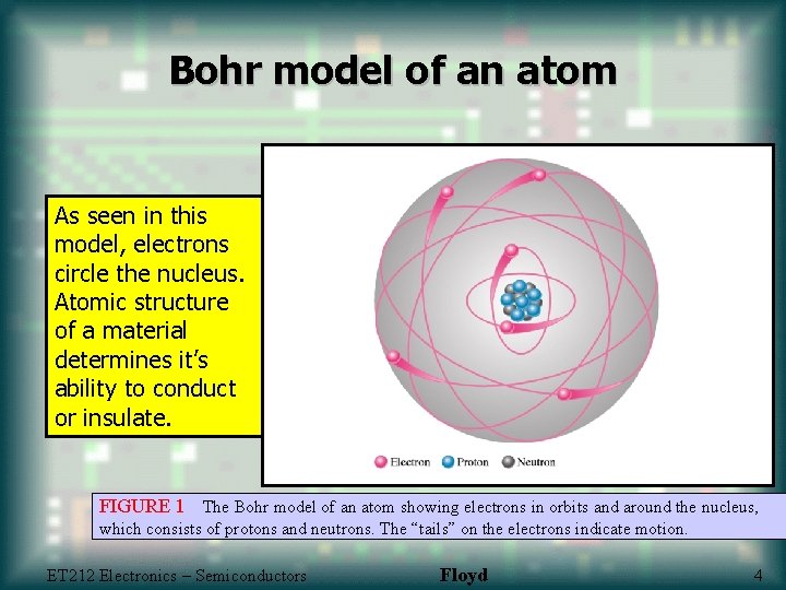
Bohr model of an atom As seen in this model, electrons circle the nucleus. Atomic structure of a material determines it’s ability to conduct or insulate. FIGURE 1 The Bohr model of an atom showing electrons in orbits and around the nucleus, which consists of protons and neutrons. The “tails” on the electrons indicate motion. ET 212 Electronics – Semiconductors Floyd 4

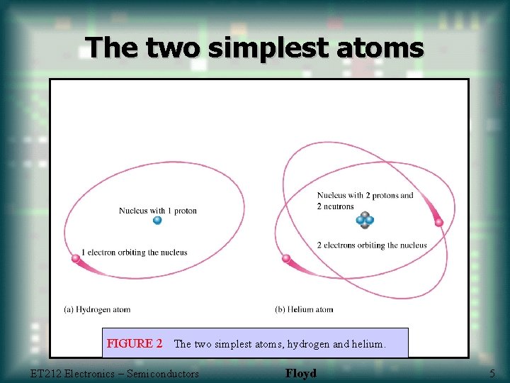
The two simplest atoms FIGURE 2 The two simplest atoms, hydrogen and helium. ET 212 Electronics – Semiconductors Floyd 5

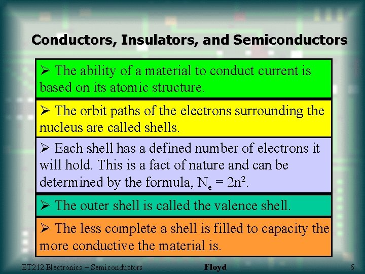
Conductors, Insulators, and Semiconductors Ø The ability of a material to conduct current is based on its atomic structure. Ø The orbit paths of the electrons surrounding the nucleus are called shells. Ø Each shell has a defined number of electrons it will hold. This is a fact of nature and can be determined by the formula, Ne = 2 n 2. Ø The outer shell is called the valence shell. Ø The less complete a shell is filled to capacity the more conductive the material is. ET 212 Electronics – Semiconductors Floyd 6

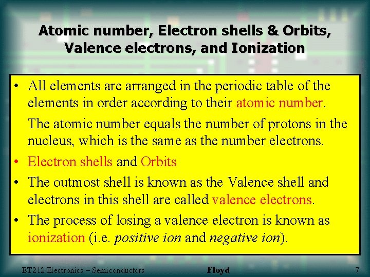
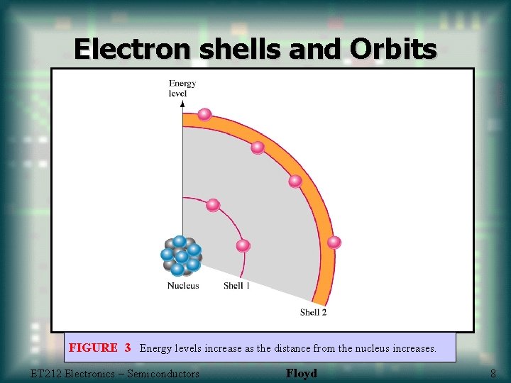
Atomic number, Electron shells & Orbits, Valence electrons, and Ionization • All elements are arranged in the periodic table of the elements in order according to their atomic number. The atomic number equals the number of protons in the nucleus, which is the same as the number electrons. • Electron shells and Orbits • The outmost shell is known as the Valence shell and electrons in this shell are called valence electrons. • The process of losing a valence electron is known as ionization (i. e. positive ion and negative ion). ET 212 Electronics – Semiconductors Floyd 7

Electron shells and Orbits FIGURE 3 Energy levels increase as the distance from the nucleus increases. ET 212 Electronics – Semiconductors Floyd 8

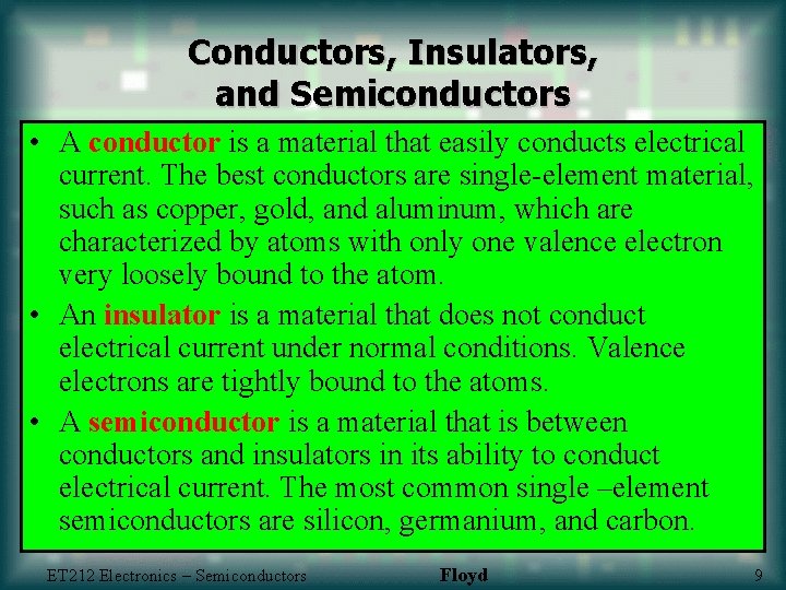
Conductors, Insulators, and Semiconductors • A conductor is a material that easily conducts electrical current. The best conductors are single-element material, such as copper, gold, and aluminum, which are characterized by atoms with only one valence electron very loosely bound to the atom. • An insulator is a material that does not conduct electrical current under normal conditions. Valence electrons are tightly bound to the atoms. • A semiconductor is a material that is between conductors and insulators in its ability to conduct electrical current. The most common single –element semiconductors are silicon, germanium, and carbon. ET 212 Electronics – Semiconductors Floyd 9

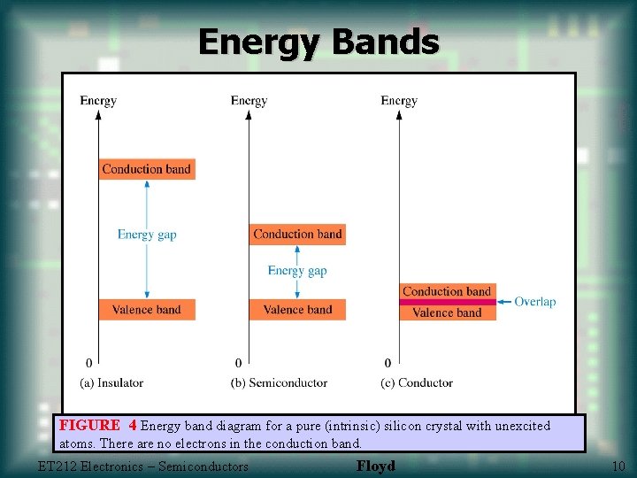
Energy Bands FIGURE 4 Energy band diagram for a pure (intrinsic) silicon crystal with unexcited atoms. There are no electrons in the conduction band. ET 212 Electronics – Semiconductors Floyd 10

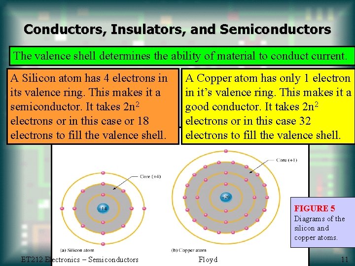
Conductors, Insulators, and Semiconductors The valence shell determines the ability of material to conduct current. A Silicon atom has 4 electrons in its valence ring. This makes it a semiconductor. It takes 2 n 2 electrons or in this case or 18 electrons to fill the valence shell. A Copper atom has only 1 electron in it’s valence ring. This makes it a good conductor. It takes 2 n 2 electrons or in this case 32 electrons to fill the valence shell. FIGURE 5 Diagrams of the silicon and copper atoms. ET 212 Electronics – Semiconductors Floyd 11

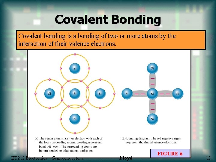
Covalent Bonding Covalent bonding is a bonding of two or more atoms by the interaction of their valence electrons. ET 212 Electronics – Semiconductors Floyd FIGURE 6 12

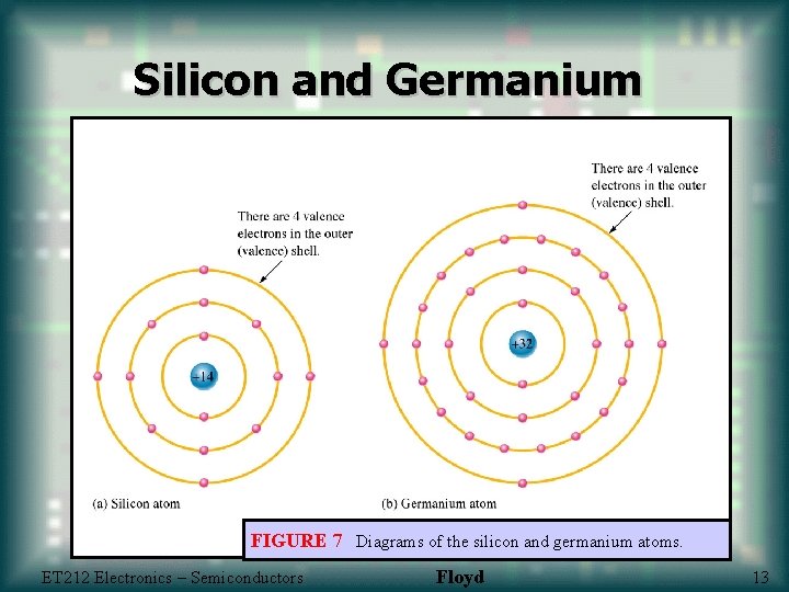
Silicon and Germanium FIGURE 7 Diagrams of the silicon and germanium atoms. ET 212 Electronics – Semiconductors Floyd 13

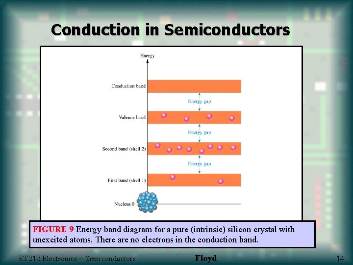
Conduction in Semiconductors FIGURE 9 Energy band diagram for a pure (intrinsic) silicon crystal with unexcited atoms. There are no electrons in the conduction band. ET 212 Electronics – Semiconductors Floyd 14

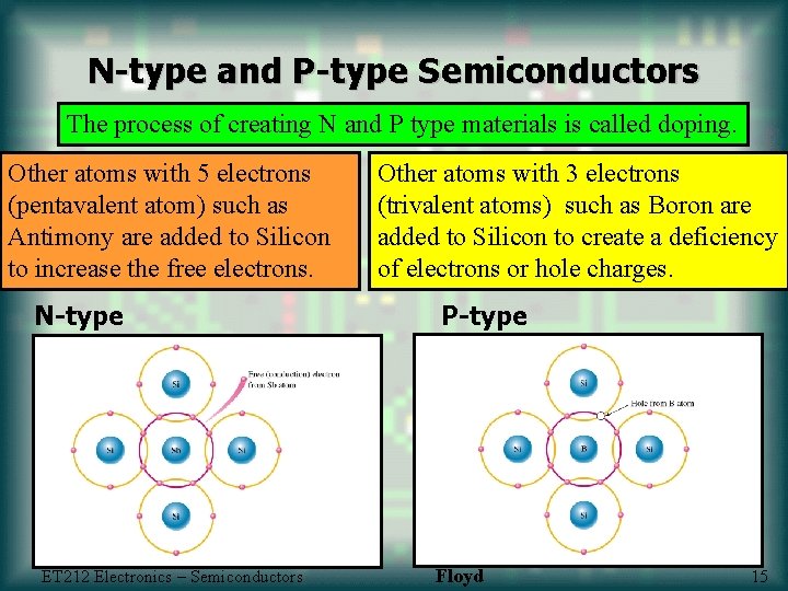
N-type and P-type Semiconductors The process of creating N and P type materials is called doping. Other atoms with 5 electrons (pentavalent atom) such as Antimony are added to Silicon to increase the free electrons. N-type ET 212 Electronics – Semiconductors Other atoms with 3 electrons (trivalent atoms) such as Boron are added to Silicon to create a deficiency of electrons or hole charges. P-type Floyd 15

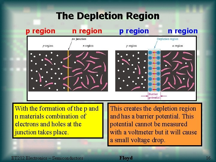
The Depletion Region p region n region With the formation of the p and n materials combination of electrons and holes at the junction takes place. ET 212 Electronics – Semiconductors p region n region This creates the depletion region and has a barrier potential. This potential cannot be measured with a voltmeter but it will cause a small voltage drop. Floyd 16

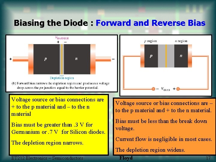
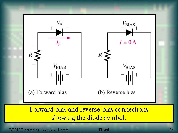
Biasing the Diode : Forward and Reverse Bias Forward Bias Voltage source or bias connections are + to the p material and – to the n material Bias must be greater than. 3 V for Germanium or. 7 V for Silicon diodes. The depletion region narrows. Reverse Bias Voltage source or bias connections are – to the p material and + to the n material. Bias must be less than the break down voltage. Current flow is negligible in most cases. The depletion region widens. ET 212 Electronics – Semiconductors Floyd 17

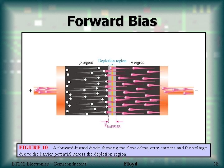
Forward Bias FIGURE 10 A forward-biased diode showing the flow of majority carriers and the voltage due to the barrier potential across the depletion region. ET 212 Electronics – Semiconductors Floyd 18

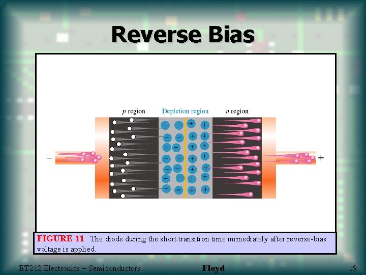
Reverse Bias FIGURE 11 The diode during the short transition time immediately after reverse-bias voltage is applied. ET 212 Electronics – Semiconductors Floyd 19

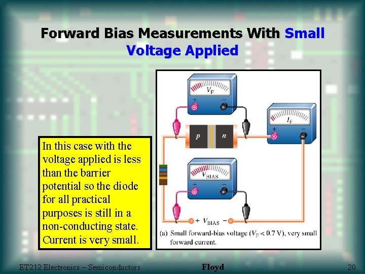
Forward Bias Measurements With Small Voltage Applied In this case with the voltage applied is less than the barrier potential so the diode for all practical purposes is still in a non-conducting state. Current is very small. ET 212 Electronics – Semiconductors Floyd 20

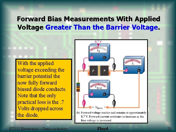
Forward Bias Measurements With Applied Voltage Greater Than the Barrier Voltage. With the applied voltage exceeding the barrier potential the now fully forward biased diode conducts. Note that the only practical loss is the. 7 Volts dropped across the diode. ET 212 Electronics – Semiconductors Floyd 21

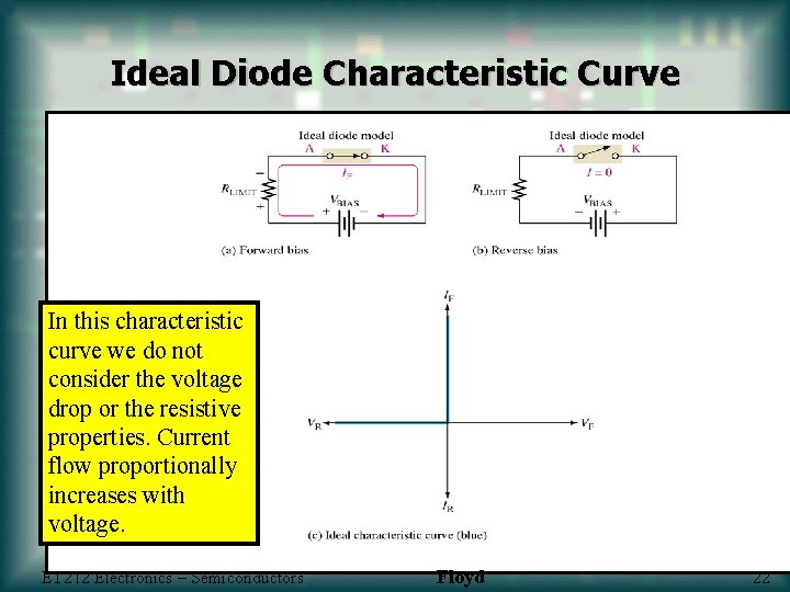
Ideal Diode Characteristic Curve In this characteristic curve we do not consider the voltage drop or the resistive properties. Current flow proportionally increases with voltage. ET 212 Electronics – Semiconductors Floyd 22

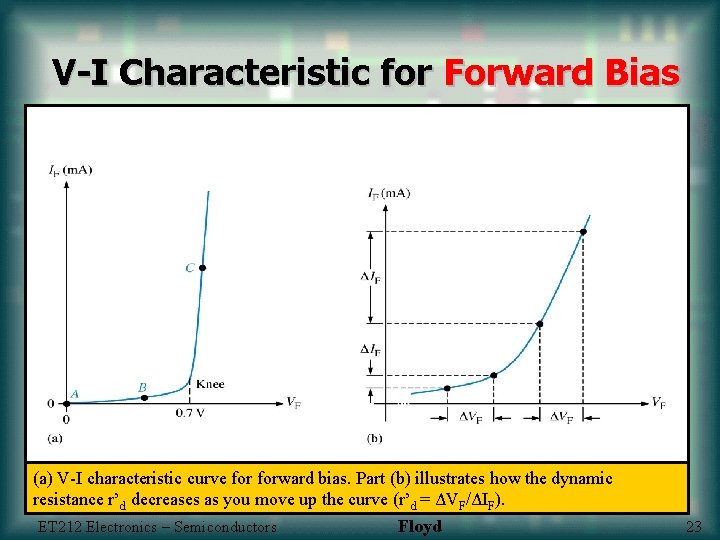
V-I Characteristic for Forward Bias (a) V-I characteristic curve forward bias. Part (b) illustrates how the dynamic resistance r’d decreases as you move up the curve (r’d = ΔVF/ΔIF). ET 212 Electronics – Semiconductors Floyd 23

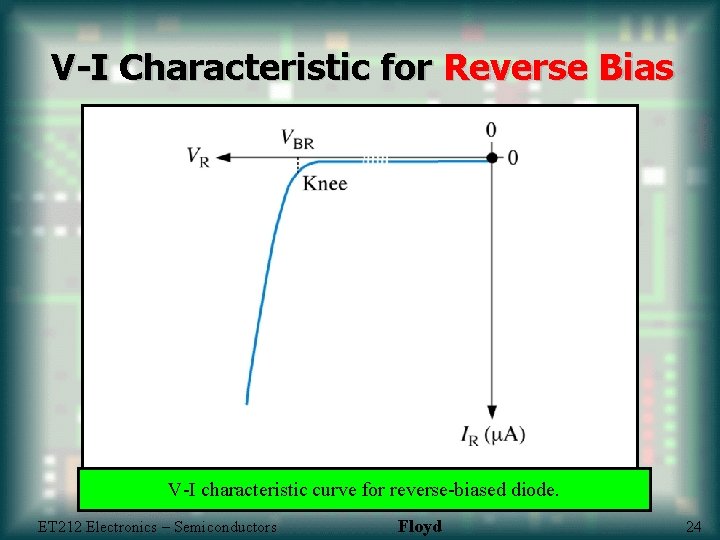
V-I Characteristic for Reverse Bias V-I characteristic curve for reverse-biased diode. ET 212 Electronics – Semiconductors Floyd 24

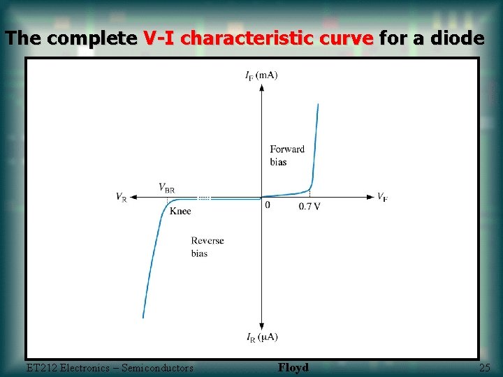
The complete V-I characteristic curve for a diode ET 212 Electronics – Semiconductors Floyd 25

Forward-bias and reverse-bias connections showing the diode symbol. ET 212 Electronics – Semiconductors Floyd 26

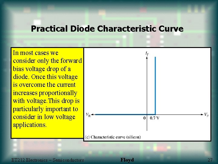
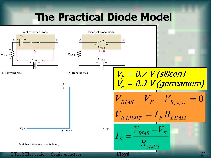
Practical Diode Characteristic Curve In most cases we consider only the forward bias voltage drop of a diode. Once this voltage is overcome the current increases proportionally with voltage. This drop is particularly important to consider in low voltage applications. ET 212 Electronics – Semiconductors Floyd 27

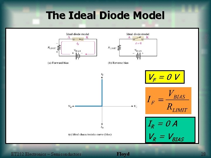
The Ideal Diode Model VF = 0 V IR = 0 A VR = VBIAS ET 212 Electronics – Semiconductors Floyd 28

The Practical Diode Model VF = 0. 7 V (silicon) VF = 0. 3 V (germanium) ET 212 Electronics – Semiconductors Floyd 29

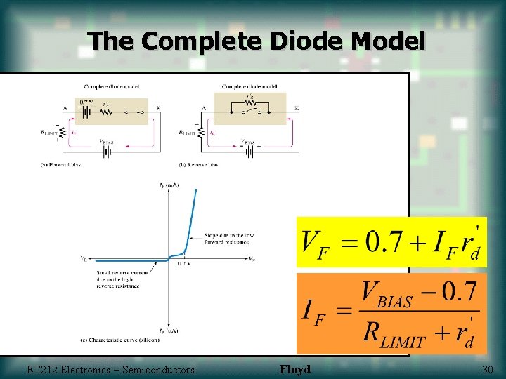
The Complete Diode Model ET 212 Electronics – Semiconductors Floyd 30

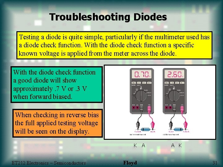
Troubleshooting Diodes Testing a diode is quite simple, particularly if the multimeter used has a diode check function. With the diode check function a specific known voltage is applied from the meter across the diode. With the diode check function a good diode will show approximately. 7 V or. 3 V when forward biased. When checking in reverse bias the full applied testing voltage will be seen on the display. K A ET 212 Electronics – Semiconductors Floyd A K 31

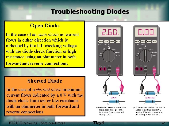
Troubleshooting Diodes Open Diode In the case of an open diode no current flows in either direction which is indicated by the full checking voltage with the diode check function or high resistance using an ohmmeter in both forward and reverse connections. Shorted Diode In the case of a shorted diode maximum current flows indicated by a 0 V with the diode check function or low resistance with an ohmmeter in both forward and reverse connections. ET 212 Electronics – Semiconductors Floyd 32