PN junction diodes Department of Electrical Electronics Engineering


- Slides: 34

PN junction diodes Department of Electrical & Electronics Engineering, Amrita School of Engineering

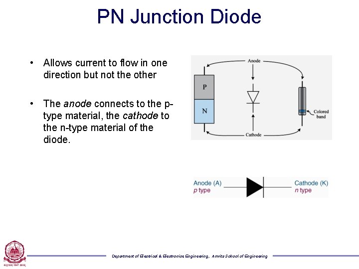
PN Junction Diode • Allows current to flow in one direction but not the other • The anode connects to the ptype material, the cathode to the n-type material of the diode. Department of Electrical & Electronics Engineering, Amrita School of Engineering

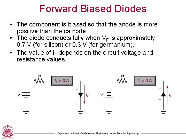
Forward Biased Diodes • The component is biased so that the anode is more positive than the cathode. • The diode conducts fully when VF is approximately 0. 7 V (for silicon) or 0. 3 V (for germanium). • The value of IF depends on the circuit voltage and resistance values. Department of Electrical & Electronics Engineering, Amrita School of Engineering

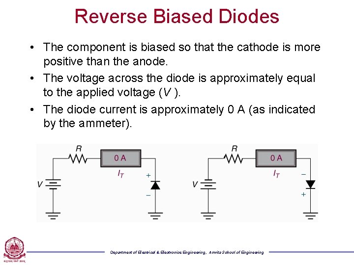
Reverse Biased Diodes • The component is biased so that the cathode is more positive than the anode. • The voltage across the diode is approximately equal to the applied voltage (V ). • The diode current is approximately 0 A (as indicated by the ammeter). Department of Electrical & Electronics Engineering, Amrita School of Engineering

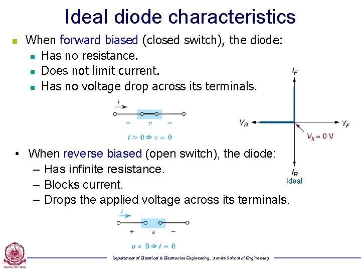
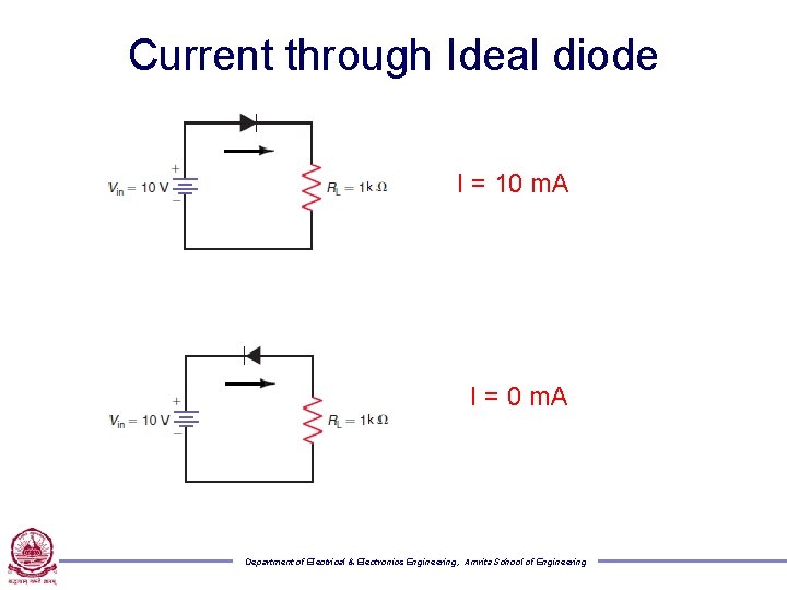
Ideal diode characteristics n When forward biased (closed switch), the diode: n Has no resistance. n Does not limit current. n Has no voltage drop across its terminals. • When reverse biased (open switch), the diode: – Has infinite resistance. – Blocks current. – Drops the applied voltage across its terminals. Department of Electrical & Electronics Engineering, Amrita School of Engineering

Current through Ideal diode I = 10 m. A I = 0 m. A Department of Electrical & Electronics Engineering, Amrita School of Engineering

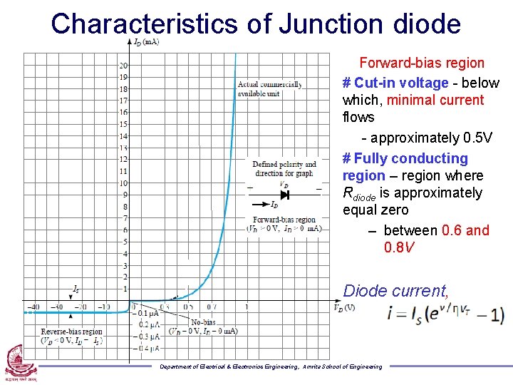
Characteristics of Junction diode Forward-bias region # Cut-in voltage - below which, minimal current flows - approximately 0. 5 V # Fully conducting region – region where Rdiode is approximately equal zero – between 0. 6 and 0. 8 V Diode current, Department of Electrical & Electronics Engineering, Amrita School of Engineering

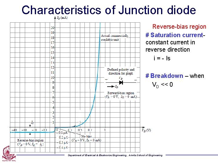
Characteristics of Junction diode Reverse-bias region # Saturation currentconstant current in reverse direction i = - Is # Breakdown – when VD << 0 Department of Electrical & Electronics Engineering, Amrita School of Engineering

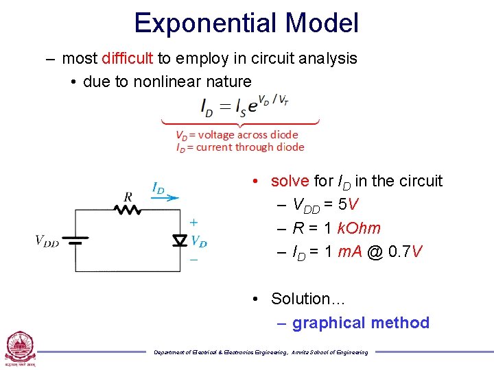
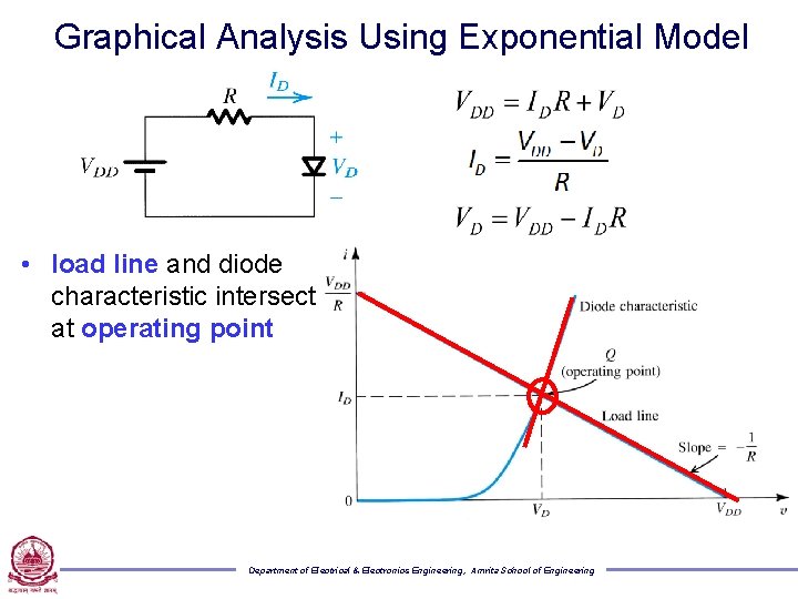
Exponential Model – most difficult to employ in circuit analysis • due to nonlinear nature • solve for ID in the circuit – VDD = 5 V – R = 1 k. Ohm – ID = 1 m. A @ 0. 7 V • Solution… – graphical method Department of Electrical & Electronics Engineering, Amrita School of Engineering

Graphical Analysis Using Exponential Model • load line and diode characteristic intersect at operating point Department of Electrical & Electronics Engineering, Amrita School of Engineering

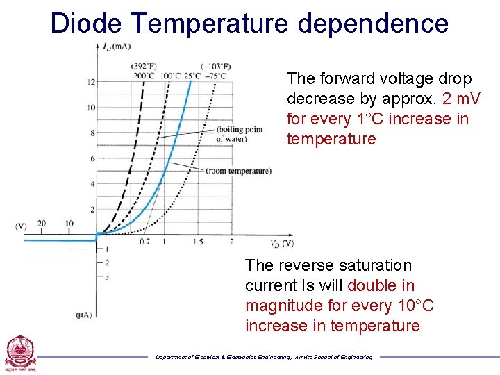
Diode Temperature dependence The forward voltage drop decrease by approx. 2 m. V for every 1°C increase in temperature The reverse saturation current Is will double in magnitude for every 10°C increase in temperature Department of Electrical & Electronics Engineering, Amrita School of Engineering

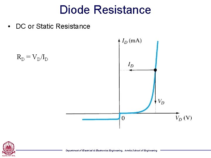
Diode Resistance • DC or Static Resistance RD = VD/ID Department of Electrical & Electronics Engineering, Amrita School of Engineering

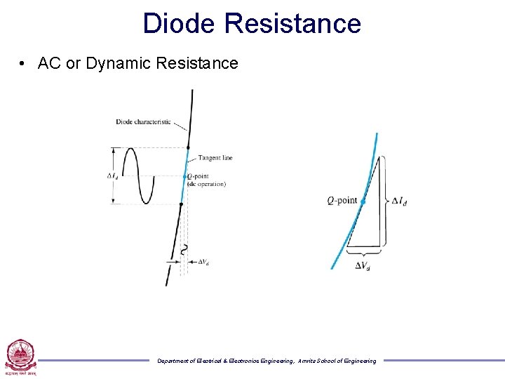
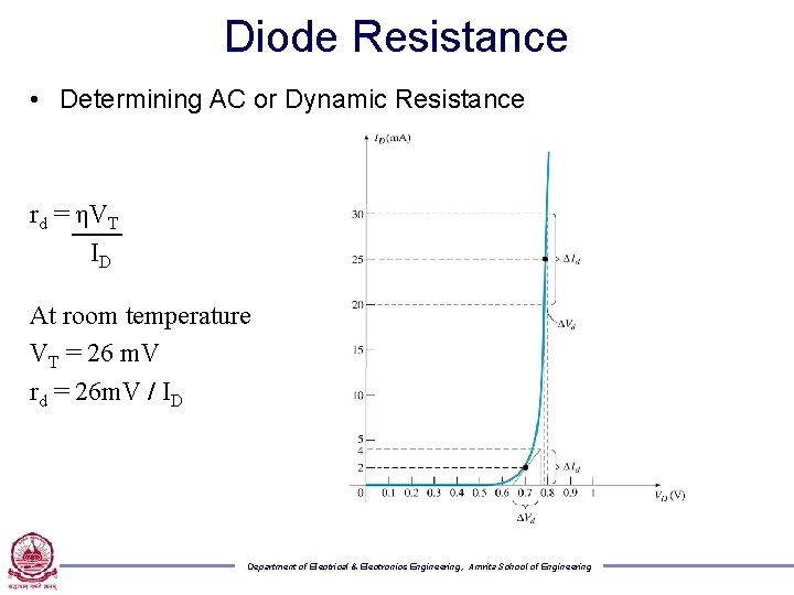
Diode Resistance • AC or Dynamic Resistance Department of Electrical & Electronics Engineering, Amrita School of Engineering

Diode Resistance • Determining AC or Dynamic Resistance rd = ηVT ID At room temperature VT = 26 m. V rd = 26 m. V / ID Department of Electrical & Electronics Engineering, Amrita School of Engineering

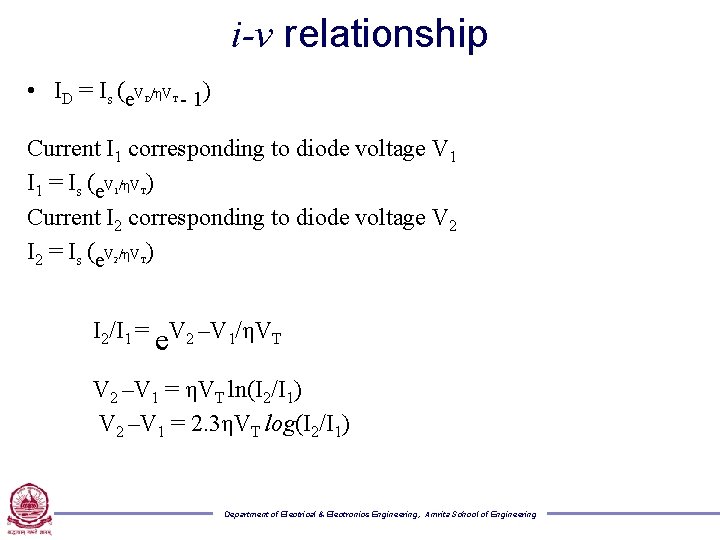
i-v relationship • ID = Is (e. V /ηV - 1) D T Current I 1 corresponding to diode voltage V 1 I 1 = Is (e. V /ηV ) Current I 2 corresponding to diode voltage V 2 I 2 = Is (e. V /ηV ) 1 T 2 T I 2/I 1 = e. V 2 –V 1/ηVT V 2 –V 1 = ηVT ln(I 2/I 1) V 2 –V 1 = 2. 3ηVT log(I 2/I 1) Department of Electrical & Electronics Engineering, Amrita School of Engineering

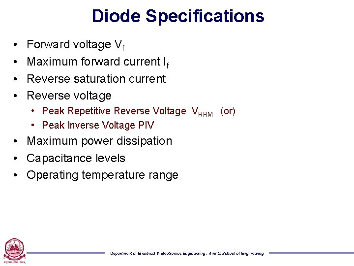
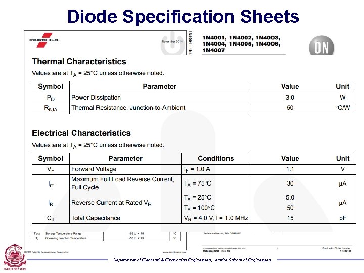
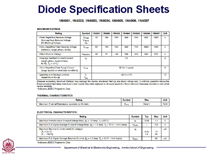
Diode Specifications • • Forward voltage Vf Maximum forward current If Reverse saturation current Reverse voltage • Peak Repetitive Reverse Voltage VRRM (or) • Peak Inverse Voltage PIV • Maximum power dissipation • Capacitance levels • Operating temperature range Department of Electrical & Electronics Engineering, Amrita School of Engineering

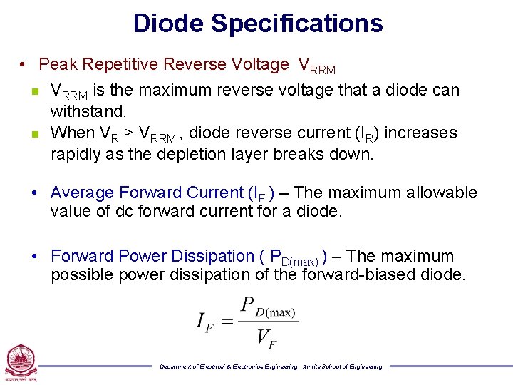
Diode Specifications • Peak Repetitive Reverse Voltage VRRM n VRRM is the maximum reverse voltage that a diode can withstand. n When VR > VRRM , diode reverse current (IR) increases rapidly as the depletion layer breaks down. • Average Forward Current (IF ) – The maximum allowable value of dc forward current for a diode. • Forward Power Dissipation ( PD(max) ) – The maximum possible power dissipation of the forward-biased diode. Department of Electrical & Electronics Engineering, Amrita School of Engineering

Diode Specification Sheets Department of Electrical & Electronics Engineering, Amrita School of Engineering

Diode Specification Sheets Department of Electrical & Electronics Engineering, Amrita School of Engineering

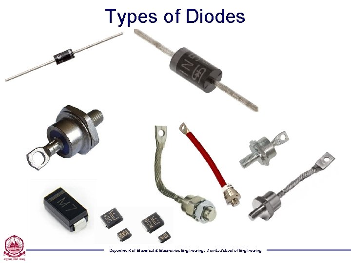
Types of Diodes Department of Electrical & Electronics Engineering, Amrita School of Engineering

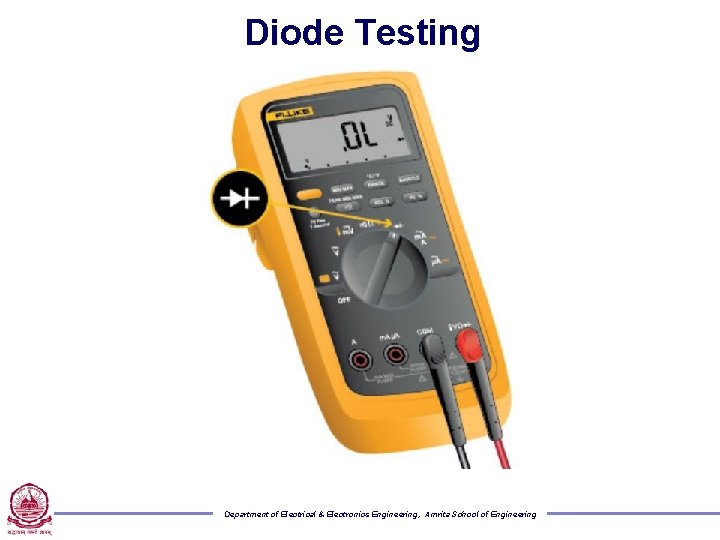
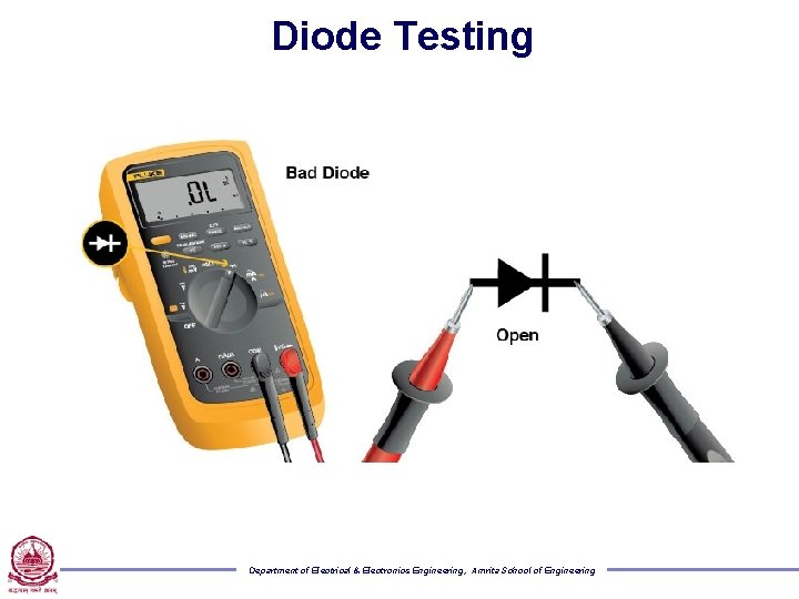
Diode Testing Department of Electrical & Electronics Engineering, Amrita School of Engineering

Diode Testing Department of Electrical & Electronics Engineering, Amrita School of Engineering

Diode Applications Department of Electrical & Electronics Engineering, Amrita School of Engineering

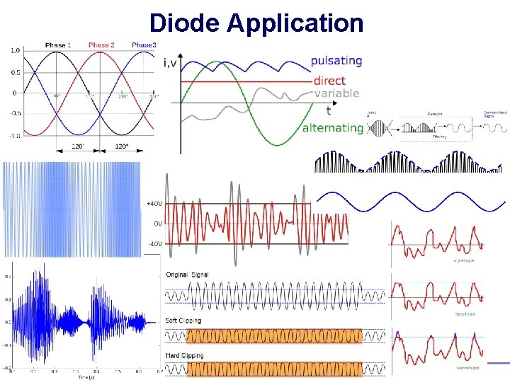
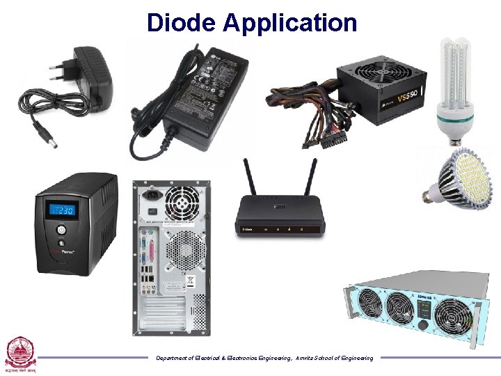
Diode Application Department of Electrical & Electronics Engineering, Amrita School of Engineering

Diode Application Department of Electrical & Electronics Engineering, Amrita School of Engineering

Clippers and Clampers Department of Electrical & Electronics Engineering, Amrita School of Engineering

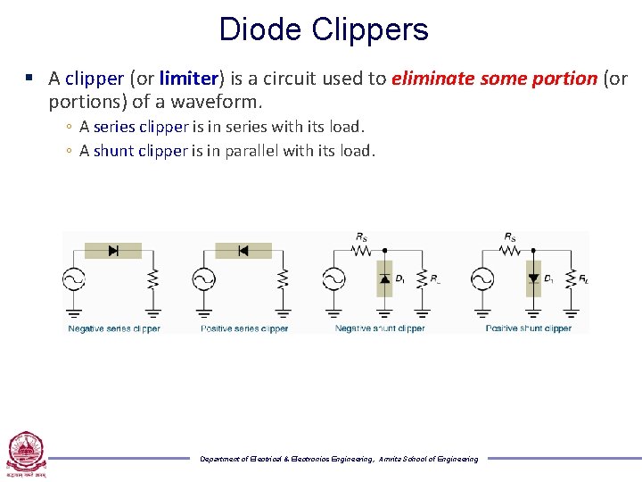
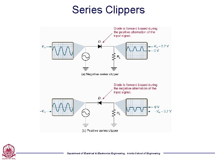
Diode Clippers § A clipper (or limiter) is a circuit used to eliminate some portion (or portions) of a waveform. ◦ A series clipper is in series with its load. ◦ A shunt clipper is in parallel with its load. Department of Electrical & Electronics Engineering, Amrita School of Engineering

Series Clippers Department of Electrical & Electronics Engineering, Amrita School of Engineering

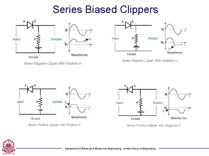
Series Biased Clippers Department of Electrical & Electronics Engineering, Amrita School of Engineering

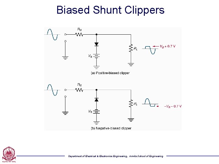
Biased Shunt Clippers Department of Electrical & Electronics Engineering, Amrita School of Engineering

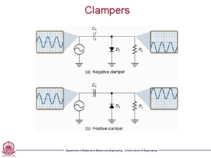
Clampers Department of Electrical & Electronics Engineering, Amrita School of Engineering

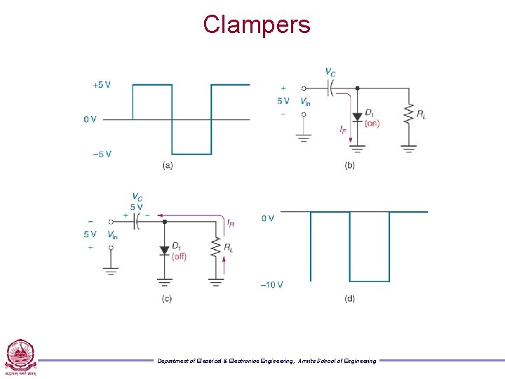
Clampers Department of Electrical & Electronics Engineering, Amrita School of Engineering

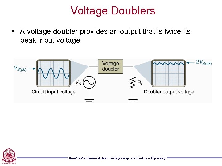
Voltage Doublers • A voltage doubler provides an output that is twice its peak input voltage. Department of Electrical & Electronics Engineering, Amrita School of Engineering

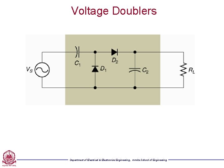
Voltage Doublers Department of Electrical & Electronics Engineering, Amrita School of Engineering