EGR 2131 Unit 7 Multiplexers and Decoders Read
- Slides: 31

EGR 2131 Unit 7 Multiplexers and Decoders Read Brown & Vranesic, Sections 6. 1 and 6. 2. ¡ Homework #7 and Lab #7 due next week. ¡ Quiz covering Units 6 and 7 next week. ¡

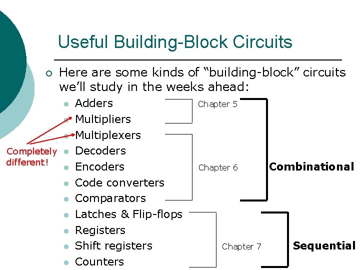
Useful Building-Block Circuits ¡ Here are some kinds of “building-block” circuits we’ll study in the weeks ahead: l l l Completely l different! l l l l Adders Multipliers Multiplexers Decoders Encoders Code converters Comparators Latches & Flip-flops Registers Shift registers Counters Chapter 5 Chapter 6 Chapter 7 Combinational Sequential

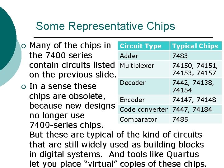
Some Representative Chips ¡ ¡ Many of the chips in Circuit Type Typical Chips the 7400 series Adder 7483 contain circuits listed Multiplexer 74150, 74151, 74153, 74157 on the previous slide. Decoder 7442, 74138, In a sense these 74154 chips are obsolete, Encoder 74147, 74148 because new designs Code converter 7447, 74184 no longer use Comparator 7485 7400 -series chips. But these are typical of the kind of circuits that are still widely used as building blocks in digital systems. And tools like Quartus let you place “virtual” copies of these chips.

Useful Building-Block Circuits (Continued) ¡ For each type of circuit listed above, you should understand: 1. 2. 3. What type of circuit does, and why it’s useful. How you could build such a circuit out of gates. Typical features found in practical circuits in each category.

Enable Pins ¡ ¡ Many of the circuits we’ll study have enable inputs. Depending on the logic level at this pin, the circuit is either enabled or disabled. When the circuit is enabled, it performs its intended function and the outputs behave as you would expect. When the circuit is disabled, then (usually) all outputs are forced to their inactive state, regardless of the other inputs to the chip. Common names for enable pins include EN, G (for “gate”), and CS (for “chip select”).

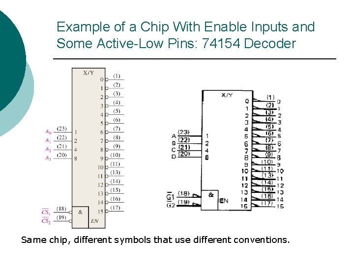
Active-High versus Active-Low Pins ¡ ¡ Each input pin and output pin on a chip is either active-high or active-low. In a logic symbol: l l ¡ ¡ Active-low pins are marked with a bubble or triangle. Active-high pins have no bubble or triangle. Active-high pins: the pin is active when there’s a HIGH on that pin. Many chips have active-low pins: the pin is active when there’s a LOW on that pin.

Example of a Chip With Enable Inputs and Some Active-Low Pins: 74154 Decoder Same chip, different symbols that use different conventions.

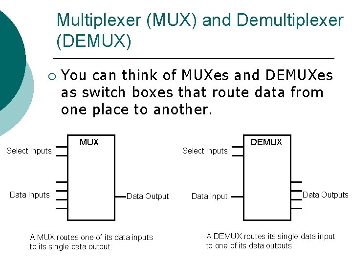
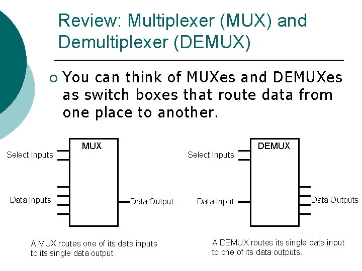
Multiplexer (MUX) and Demultiplexer (DEMUX) ¡ Select Inputs Data Inputs You can think of MUXes and DEMUXes as switch boxes that route data from one place to another. MUX Select Inputs Data Output A MUX routes one of its data inputs to its single data output. Data Input DEMUX Data Outputs A DEMUX routes its single data input to one of its data outputs.

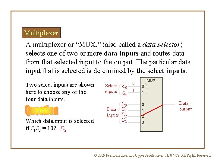
Multiplexer A multiplexer or “MUX, ” (also called a data selector) selects one of two or more data inputs and routes data from that selected input to the output. The particular data input that is selected is determined by the select inputs. Two select inputs are shown here to choose any of the four data inputs. Which data input is selected if S 1 S 0 = 10? D 2 Select inputs S 0 S 1 D 0 Data D 1 inputs D 2 D 3 0 1 Data output © 2009 Pearson Education, Upper Saddle River, NJ 07458. All Rights Reserved

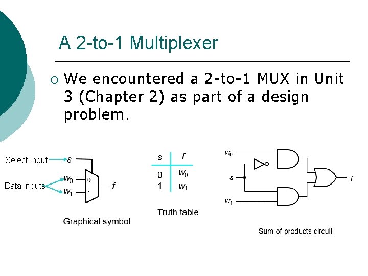
A 2 -to-1 Multiplexer ¡ Select input Data inputs We encountered a 2 -to-1 MUX in Unit 3 (Chapter 2) as part of a design problem.

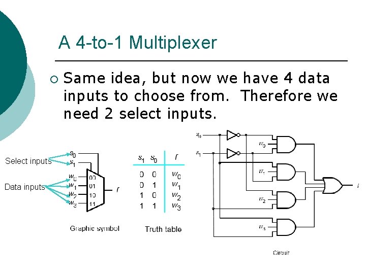
A 4 -to-1 Multiplexer ¡ Select inputs Data inputs Same idea, but now we have 4 data inputs to choose from. Therefore we need 2 select inputs.

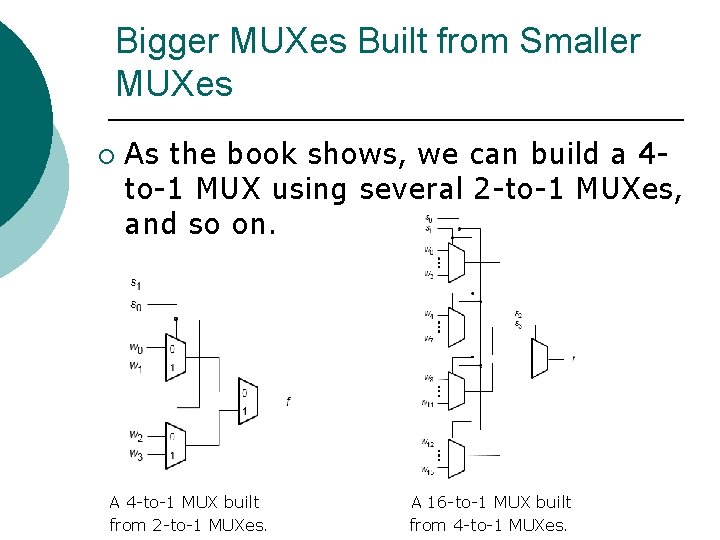
Bigger MUXes Built from Smaller MUXes ¡ As the book shows, we can build a 4 to-1 MUX using several 2 -to-1 MUXes, and so on. A 4 -to-1 MUX built from 2 -to-1 MUXes. A 16 -to-1 MUX built from 4 -to-1 MUXes.

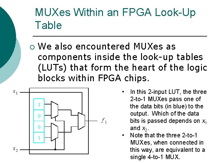
MUXes Within an FPGA Look-Up Table ¡ We also encountered MUXes as components inside the look-up tables (LUTs) that form the heart of the logic blocks within FPGA chips. • In this 2 -input LUT, the three 2 -to-1 MUXes pass one of the data bits (in blue) to the output. Which of the data bits is passed depends on x 1 and x 2. • Note that the three 2 -to-1 MUXes, when connected in this way, are equivalent to a single 4 -to-1 MUX.

Some 74 xx Multiplexer Chips 74150 ¡ 74151 ¡ 74153 ¡ 74157 ¡ (16 -input MUX) (8 -input MUX) (dual 4 -input MUX) (quad 2 -input MUX)

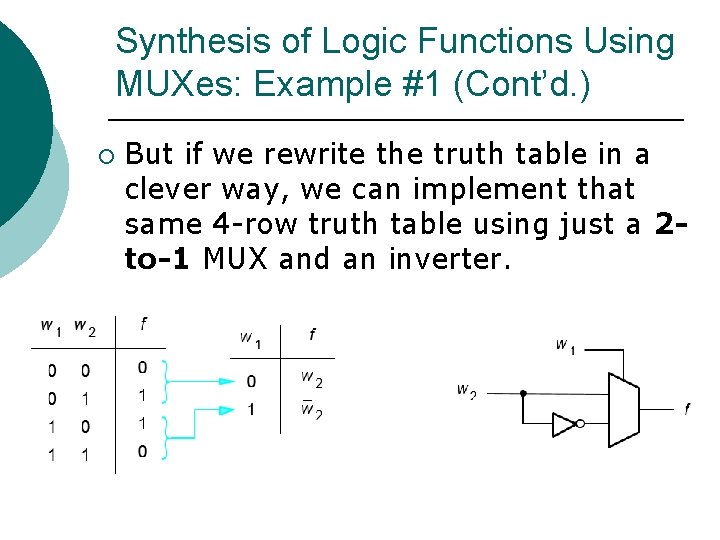
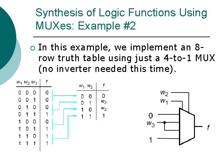
Synthesis of Logic Functions Using MUXes Many applications make straightforward use of MUXes as switch boxes. ¡ But MUXes are also often used in another way, as general-purpose “logic machines”: you can implement any nrow truth table using an (n-divided-by 2)-to-1 MUX and an inverter, rather than using our K-map-based design procedure to implement it using gates. ¡

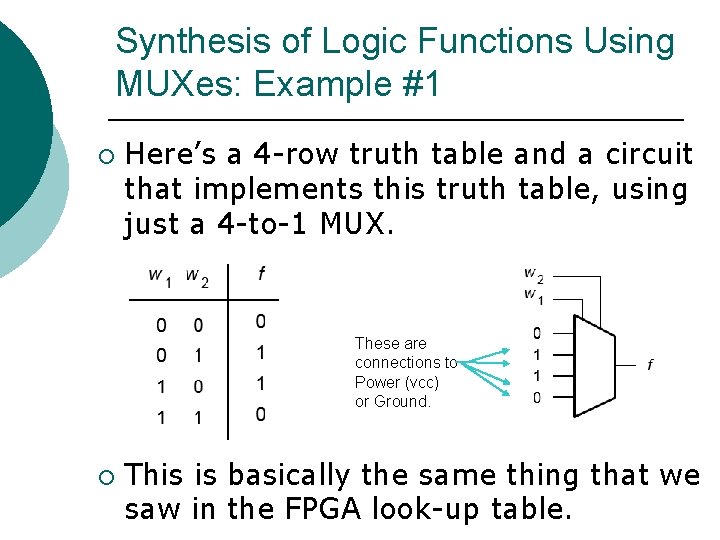
Synthesis of Logic Functions Using MUXes: Example #1 ¡ Here’s a 4 -row truth table and a circuit that implements this truth table, using just a 4 -to-1 MUX. These are connections to Power (vcc) or Ground. ¡ This is basically the same thing that we saw in the FPGA look-up table.

Synthesis of Logic Functions Using MUXes: Example #1 (Cont’d. ) ¡ But if we rewrite the truth table in a clever way, we can implement that same 4 -row truth table using just a 2 to-1 MUX and an inverter.

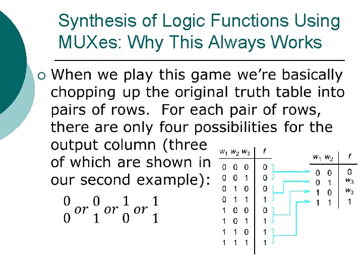
Synthesis of Logic Functions Using MUXes: Example #2 ¡ In this example, we implement an 8 row truth table using just a 4 -to-1 MUX (no inverter needed this time).

Synthesis of Logic Functions Using MUXes: Why This Always Works ¡

For Further Study: Shannon’s Expansion Theorem We’ve been using MUXes to implement general logic functions. An extension of this topic involves Shannon’s expansion theorem, which can help you to find even more efficient implementations using MUXes (and additional gates). ¡ The book discusses it, and it’s very useful, but not a topic that we’ll need in this introductory course. ¡

Decoders, Encoders, & Code Converters Decoders convert a binary code into a single active output representing that code’s value. ¡ Encoders generate a coded output from a single active input line. ¡ Code converters take one input code (such as BCD) and convert it to another code (such as binary). ¡

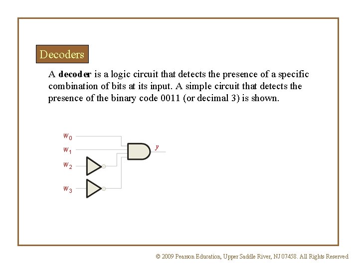
Decoders A decoder is a logic circuit that detects the presence of a specific combination of bits at its input. A simple circuit that detects the presence of the binary code 0011 (or decimal 3) is shown. w 0 w 1 y w 2 w 3 © 2009 Pearson Education, Upper Saddle River, NJ 07458. All Rights Reserved

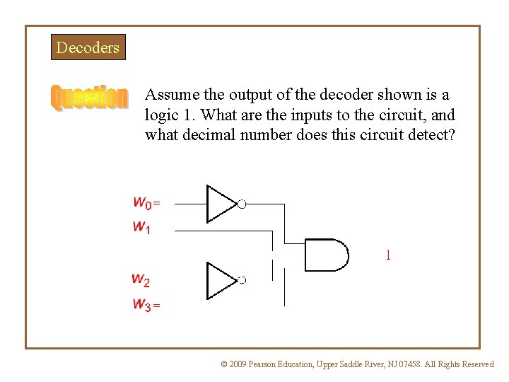
Decoders Assume the output of the decoder shown is a logic 1. What are the inputs to the circuit, and what decimal number does this circuit detect? © 2009 Pearson Education, Upper Saddle River, NJ 07458. All Rights Reserved

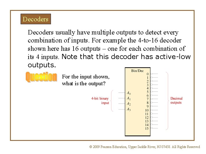
Decoders usually have multiple outputs to detect every combination of inputs. For example the 4 -to-16 decoder shown here has 16 outputs – one for each combination of its 4 inputs. Note that this decoder has active-low outputs. For the input shown, what is the output? © 2009 Pearson Education, Upper Saddle River, NJ 07458. All Rights Reserved

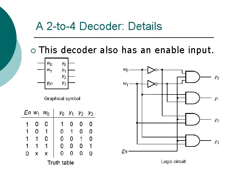
A 2 -to-4 Decoder: Details ¡ This decoder also has an enable input.

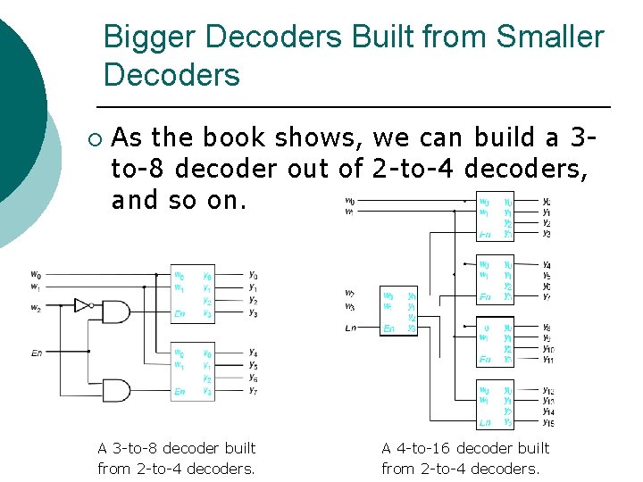
Bigger Decoders Built from Smaller Decoders ¡ As the book shows, we can build a 3 to-8 decoder out of 2 -to-4 decoders, and so on. A 3 -to-8 decoder built from 2 -to-4 decoders. A 4 -to-16 decoder built from 2 -to-4 decoders.

Synthesis of Logic Functions Using Decoders ¡ Like MUXes, decoders can serve as general-purpose “logic machines”: you can implement any n-input truth table using an n-input decoder and an OR gate, rather than using our K-mapbased design procedure to implement it using gates. l Note that in general this is not very efficient, since the decoder likely has many more gates than needed to implement the function.

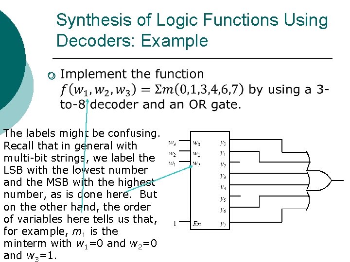
Synthesis of Logic Functions Using Decoders: Example ¡ The labels might be confusing. Recall that in general with multi-bit strings, we label the LSB with the lowest number and the MSB with the highest number, as is done here. But on the other hand, the order of variables here tells us that, for example, m 1 is the minterm with w 1=0 and w 2=0 and w 3=1.

Some 74 xx Decoder Chips 74138 3 -to-8 decoder (“octal” decoder) ¡ 74154 4 -to-16 decoder (“hex” decoder) ¡ 7442 4 -to-10 decoder (“BCD” decoder) ¡ l You would use a BCD decoder rather than a hex decoder in cases where you know that the input variables can never form a number greater than decimal 9 (binary 1001).

Review: Multiplexer (MUX) and Demultiplexer (DEMUX) ¡ Select Inputs Data Inputs You can think of MUXes and DEMUXes as switch boxes that route data from one place to another. MUX Select Inputs Data Output A MUX routes one of its data inputs to its single data output. Data Input DEMUX Data Outputs A DEMUX routes its single data input to one of its data outputs.

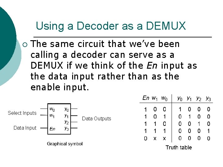
Using a Decoder as a DEMUX ¡ The same circuit that we’ve been calling a decoder can serve as a DEMUX if we think of the En input as the data input rather than as the enable input. Select Inputs Data Outputs Data Input