Differential 2 R Crosspoint RRAM for Memory system

![Differential 2 R cell 1 cell WLa[1] BL 0 BL 1 BL 2 + Differential 2 R cell 1 cell WLa[1] BL 0 BL 1 BL 2 +](https://slidetodoc.com/presentation_image_h2/44d78884acb0721ceba4697811606cdf/image-7.jpg)


- Slides: 16

Differential 2 R Crosspoint RRAM for Memory system in Mobile Electronics with Zero Standby Current Pi-Feng Chiu, Pengpeng Lu, Zeying Xin EECS, UC Berkeley 05/06/2013

Outline • Introduction o Memory Hierarchy o RRAM switching mechanism • Issues of Crosspoint Array • Proposed Differential 2 R cell o Cell Characteristics o Differential 2 R cell and array design • Circuit Implementation o Divided WL and Sense-before • Simulation Results • Comparison • Conclusion

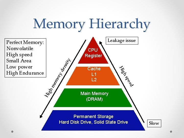
Memory Hierarchy Leakage issue Perfect Memory: Nonvolatile High speed Small Area Low power High Endurance ry d me mo gh eed sp Hi gh Cache L 1 L 2 Hi en sit y CPU Register Main Memory (DRAM) Permanent Storage Hard Disk Drive, Solid State Drive Slow

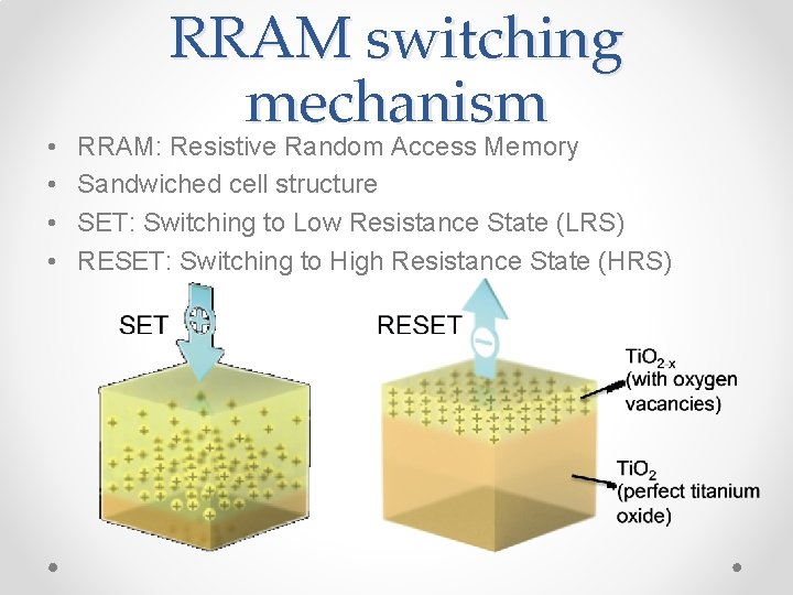
• • RRAM switching mechanism RRAM: Resistive Random Access Memory Sandwiched cell structure SET: Switching to Low Resistance State (LRS) RESET: Switching to High Resistance State (HRS)

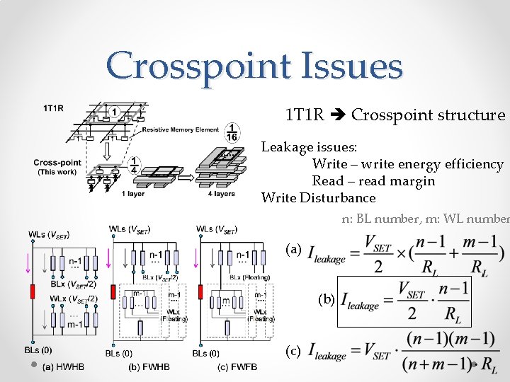
Crosspoint Issues 1 T 1 R Crosspoint structure Leakage issues: Write – write energy efficiency Read – read margin Write Disturbance n: BL number, m: WL number (a) (b) (c)

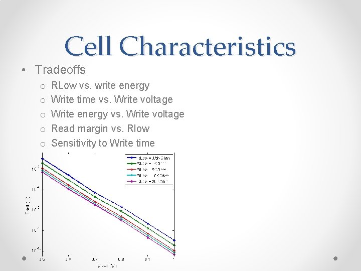
Cell Characteristics • Tradeoffs o o o RLow vs. write energy Write time vs. Write voltage Write energy vs. Write voltage Read margin vs. Rlow Sensitivity to Write time
![Differential 2 R cell 1 cell WLa1 BL 0 BL 1 BL 2 Differential 2 R cell 1 cell WLa[1] BL 0 BL 1 BL 2 +](https://slidetodoc.com/presentation_image_h2/44d78884acb0721ceba4697811606cdf/image-7.jpg)
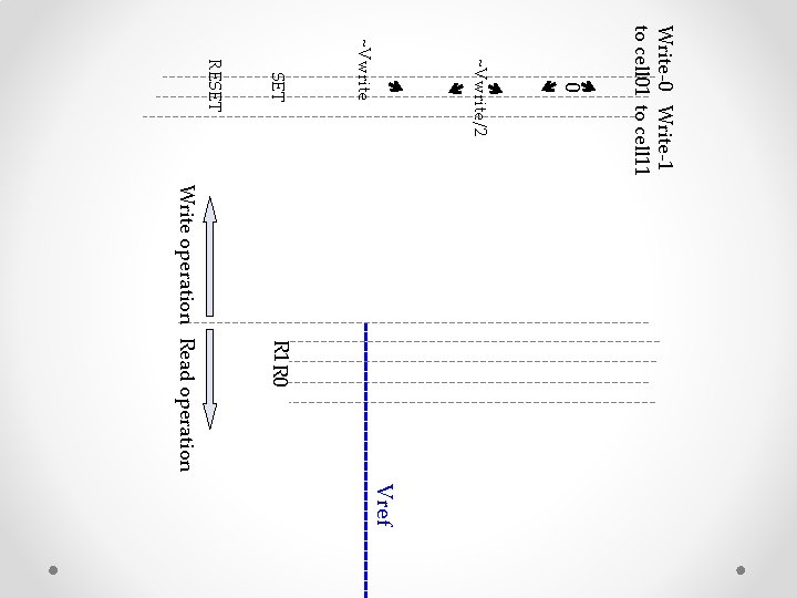
Differential 2 R cell 1 cell WLa[1] BL 0 BL 1 BL 2 + In read operation, WLa=Vread, WLb=0 Voltage-sensing VBL + VBL=Vread*Rb/(Ra+Rb) Ra Rb WLb[1] WLa[0] WLb[0] - Write-1 Write-0 Ra SET RESET Rb RESET WL Vwrite 0 BL 0 Vwrite Assumption: VSET=VRESET=Vwrite

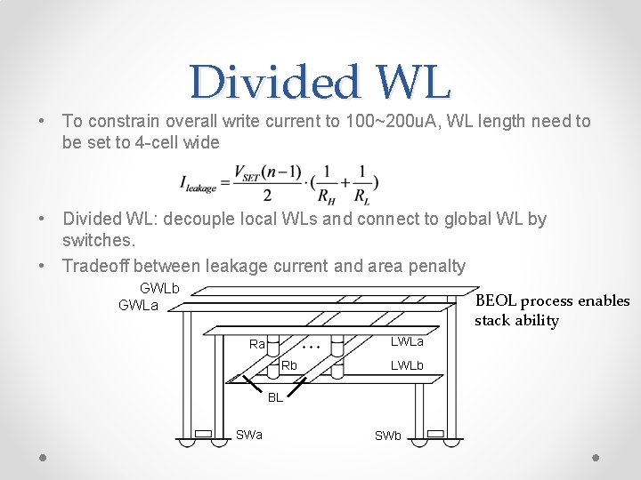
Divided WL • To constrain overall write current to 100~200 u. A, WL length need to be set to 4 -cell wide • Divided WL: decouple local WLs and connect to global WL by switches. • Tradeoff between leakage current and area penalty GWLb GWLa … Ra Rb BEOL process enables stack ability LWLa LWLb BL SWa SWb

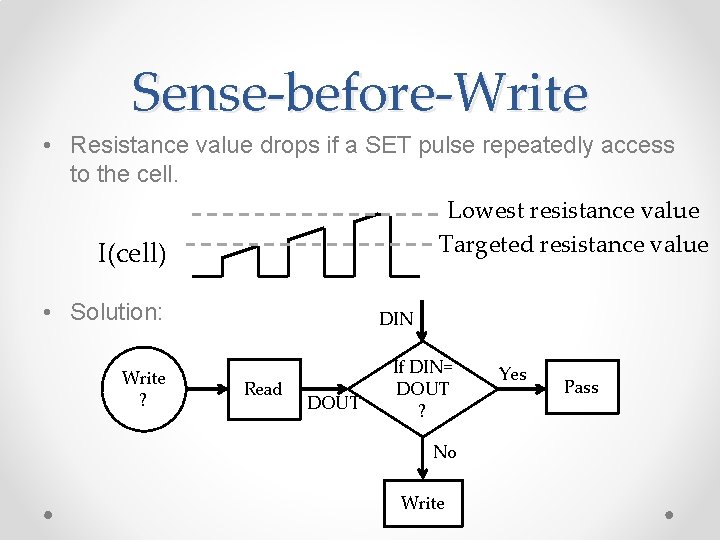
Sense-before-Write • Resistance value drops if a SET pulse repeatedly access to the cell. Lowest resistance value Targeted resistance value I(cell) • Solution: Write ? DIN Read DOUT If DIN= DOUT ? No Write Yes Pass

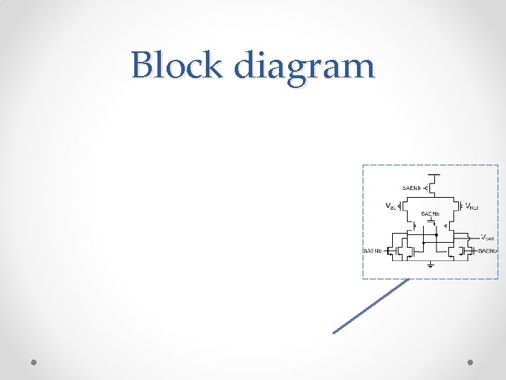
Block diagram

Write-0 Write-1 to cell 01 to cell 11 0 ~Vwrite/2 ~Vwrite SET RESET R 1 R 0 Write operation Read operation Vref

Features

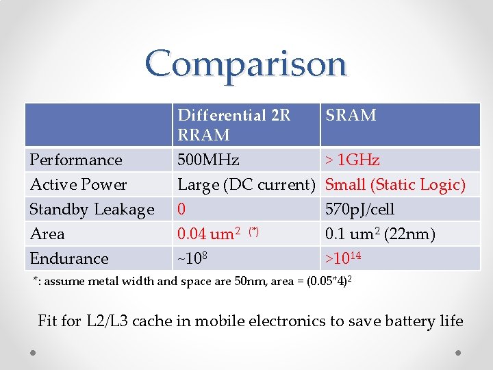
Comparison Performance Active Power Standby Leakage Area Endurance Differential 2 R RRAM SRAM 500 MHz Large (DC current) 0 0. 04 um 2 (*) ~108 > 1 GHz Small (Static Logic) 570 p. J/cell 0. 1 um 2 (22 nm) >1014 *: assume metal width and space are 50 nm, area = (0. 05*4)2 Fit for L 2/L 3 cache in mobile electronics to save battery life

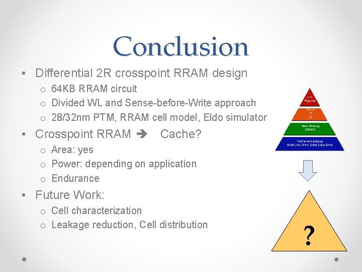
Conclusion • Differential 2 R crosspoint RRAM design o 64 KB RRAM circuit o Divided WL and Sense-before-Write approach o 28/32 nm PTM, RRAM cell model, Eldo simulator • Crosspoint RRAM Cache? o Area: yes o Power: depending on application o Endurance • Future Work: o Cell characterization o Leakage reduction, Cell distribution ?

Thanks!

• • • Reference ITRS Roadmap (http: //www. itri. net) Yan Li, et al. , “ 128 Gb 3 b/cell NAND Flash Memory in 19 nm Technology with 18 MB/s Write Rate and 400 Mb/s Toggle Mode, ” in IEEE Int. Solid-State Circuits Conf. (ISSCC) Dig. Tech. Papers, Feb. 2012, pp. 436 -437. T. Takashima, et al. , “A 100 MHz Ladder Fe. RAM Design With Capacitance-Coupled-Bitline (CCB) Cell, ” IEEE Journal of Solid-State Circuits, Vol. 46, No. 3, March 2011. T. Shigibayashi, et al. , “A 16 -Mb Toggle MRAM With Burst Modes, ” IEEE Journal of Solid-State Circuits, Vol. 42, No. 11, Nov. 2007. D. C. Ralph and M. D. Stiles, “Spin Transfer Torques, ” Journal of Magnetism and Magnetic Materials, vol. 320, issue 7, pp. 1190 -1216, April 2008. R. E. Simpson, et al. , “Toward the Ultimate Limit of Phase Change in Ge 2 Sb 2 Te 5, ” Nano Letter, pp. 414419, 2010. Elaine Ou and S. Simon Wong, “Array Architecture for a Nonvolatile 3 -Dimensional Cross-Point Resistance-Change Memory, ” IEEE J. Solid-State Circuits, vol. 46, no. 9, pp. 2158 -2170, Sep. 2011. R. Stanley Williams, “How we found the missing memristor, ” IEEE Spectrum, vol. 45, no. 12, pp. 28 -35, 2008. A. Kawahara, et al. , “An 8 Mb Multi-Layered Cross-Point Re. RAM Macro With 443 MB/s Write Throughput, ” IEEE Journal of Solid-State Circuits, Vol. 48, No. 1, January 2013. D. Niu, C. Xu, N. Muralimanohar, N. P. Jouppi, Y. Xie, “Design Trade-Offs for High Density Cross-Point Resistive Memory, ” ISLPED, 2012, pp. 209 -214. M. Yoshimoto, et al. , “A Divided Word-line Structure in the Static SRAM and Its Application to a 64 K Full CMOS RAM” IEEE Journal of Solid-State Circuits, Vol. 18, No. 5, Oct. 1983. P. Packan, et al. , “High Performance 32 nm logic technology featuring 2 nd generation high-k + metal gate transistors, ” in Int. Electron Devices Meeting (IEDM) Tech. Dig. Papers, Dec. 2009, pp. 659 -662.