Diamond Amplified Photocathodes Preparation and Capsule Formation John
- Slides: 28

Diamond Amplified Photocathodes Preparation and Capsule Formation John Smedley 10/4/06 Workshop on High QE Milan

Collaborators I. Ben-Zvi R. Hemley, CI, Washington A. Burrill Z. Liu, CI, Washington X. Chang J. Grimes T. Rao Z. Segelov Q. Wu 10/4/06 S. Krasnicki CI, Washington K. Jenson, NRL, Washington J. Yater, NRL, Washington R. Stone, Rutgers U J. Bohon, Case Western U P. Stephens, SUNY SB Workshop on High QE Milan

Overview • • The DAP concept & capsule cathodes Diamond options Diamond preparation Secondary Yield Measurements Transparent cathode preparation Capsule fabrication Thinning diamond 10/4/06 Workshop on High QE Milan

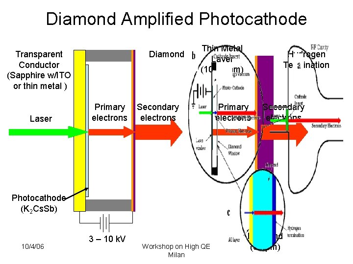
Diamond Amplified Photocathode Transparent Conductor (Sapphire w/ITO or thin metal ) Laser Diamond Primary electrons Thin Metal Layer (10 -30 nm) Secondary electrons Hydrogen Termination Primary electrons Secondary electrons Photocathode (K 2 Cs. Sb) 10/4/06 3 – 10 k. V Workshop on High QE Milan Diamond (30 μm)

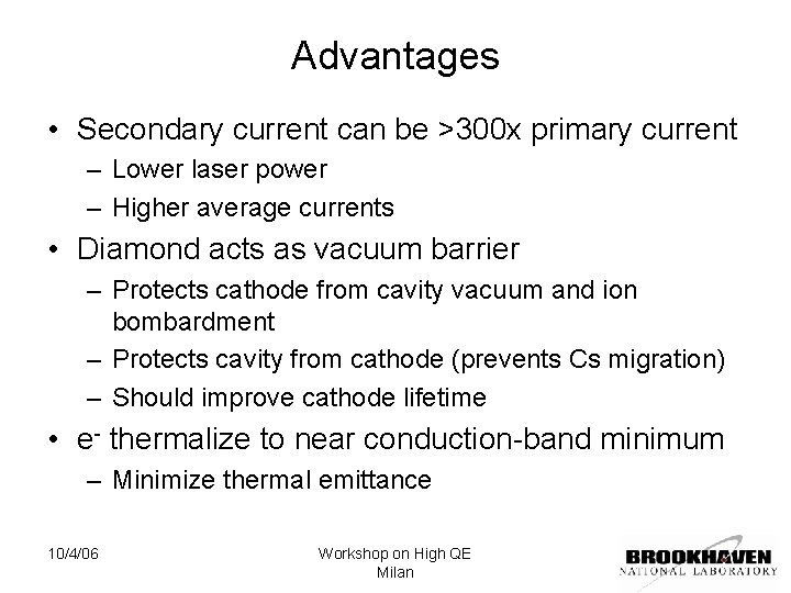
Advantages • Secondary current can be >300 x primary current – Lower laser power – Higher average currents • Diamond acts as vacuum barrier – Protects cathode from cavity vacuum and ion bombardment – Protects cavity from cathode (prevents Cs migration) – Should improve cathode lifetime • e- thermalize to near conduction-band minimum – Minimize thermal emittance 10/4/06 Workshop on High QE Milan

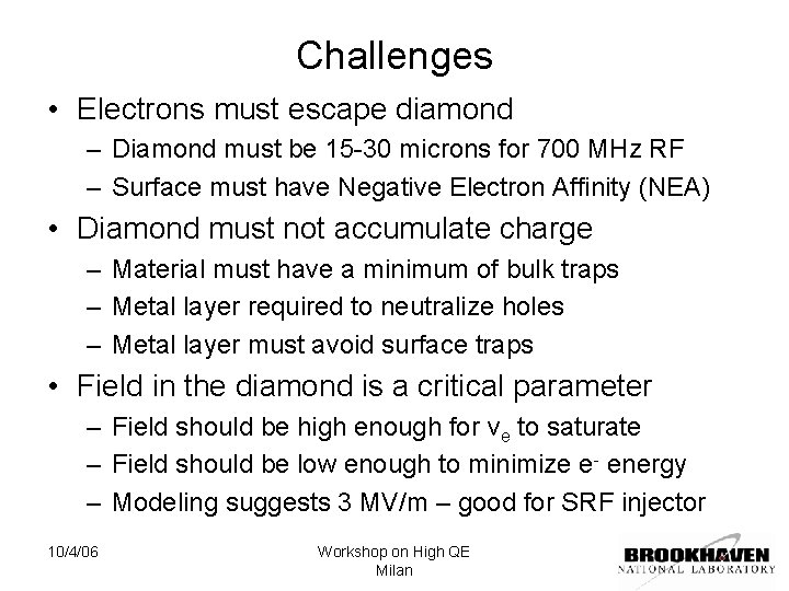
Challenges • Electrons must escape diamond – Diamond must be 15 -30 microns for 700 MHz RF – Surface must have Negative Electron Affinity (NEA) • Diamond must not accumulate charge – Material must have a minimum of bulk traps – Metal layer required to neutralize holes – Metal layer must avoid surface traps • Field in the diamond is a critical parameter – Field should be high enough for ve to saturate – Field should be low enough to minimize e- energy – Modeling suggests 3 MV/m – good for SRF injector 10/4/06 Workshop on High QE Milan

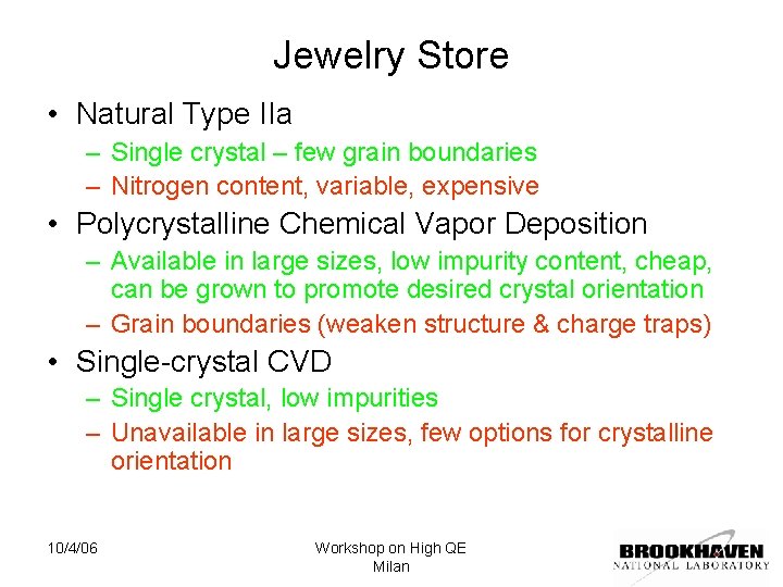
Jewelry Store • Natural Type IIa – Single crystal – few grain boundaries – Nitrogen content, variable, expensive • Polycrystalline Chemical Vapor Deposition – Available in large sizes, low impurity content, cheap, can be grown to promote desired crystal orientation – Grain boundaries (weaken structure & charge traps) • Single-crystal CVD – Single crystal, low impurities – Unavailable in large sizes, few options for crystalline orientation 10/4/06 Workshop on High QE Milan

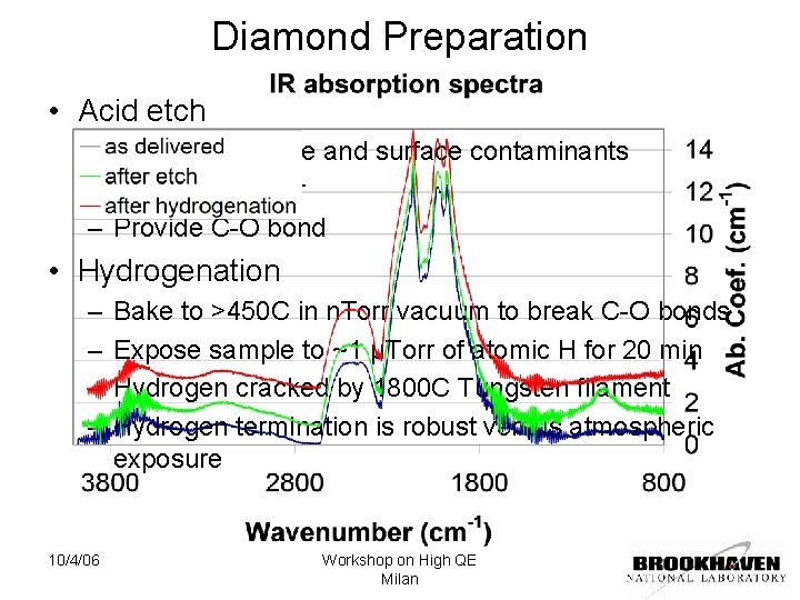
Diamond Preparation • Acid etch – Remove graphite and surface contaminants – Strip metal layer – Provide C-O bond • Hydrogenation – – 10/4/06 Bake to >450 C in n. Torr vacuum to break C-O bonds Expose sample to ~1 μTorr of atomic H for 20 min Hydrogen cracked by 1800 C Tungsten filament Hydrogen termination is robust versus atmospheric exposure Workshop on High QE Milan

Diamond Preparation - Metallization • Initial layer must bond well to diamond – Titanium forms Ti-C layer • Subsequent layers – Protect titanium from oxidation – High conductivity – Low electron stopping power (Low Z) • Ti-Pt sputtering is a common choice for diamond detectors; we have had some success with gold • We may use Ti-Pt-Al, with 5 nm of Ti, 5 nm Pt and 20 nm Al • Possibly thicker layer near the perimeter 10/4/06 Workshop on High QE Milan

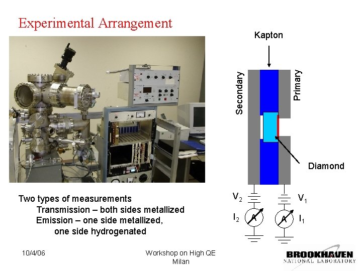
Experimental Arrangement Secondary Primary Kapton Diamond Two types of measurements Transmission – both sides metallized Emission – one side metallized, one side hydrogenated 10/4/06 Workshop on High QE Milan V 2 I 2 V 1 A A I 1

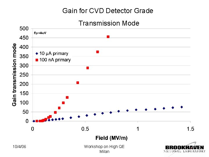
Gain for CVD Detector Grade Transmission Mode 10/4/06 Workshop on High QE Milan

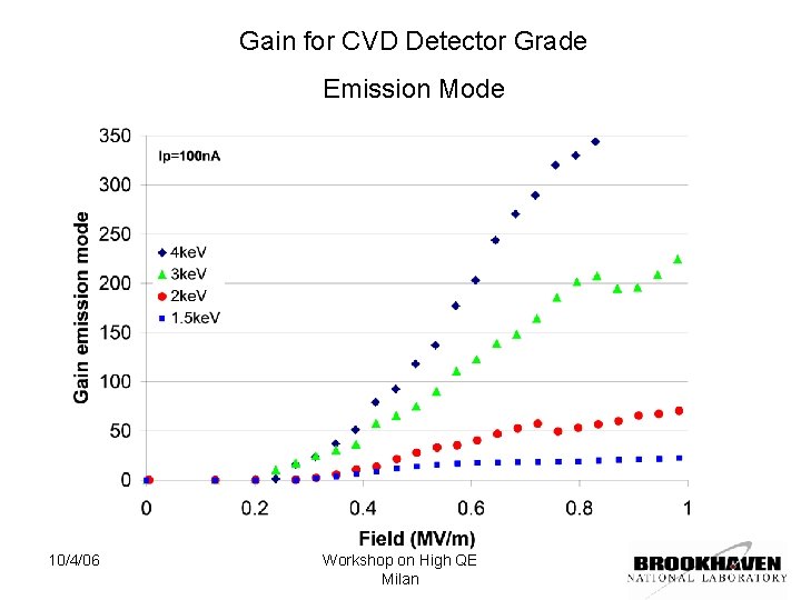
Gain for CVD Detector Grade Emission Mode 10/4/06 Workshop on High QE Milan

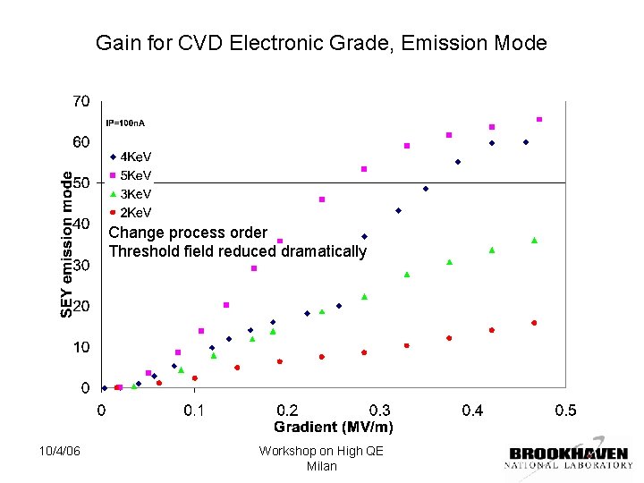
Gain for CVD Electronic Grade, Emission Mode Large emission threshold implies charge trapping Change process order Threshold field reduced dramatically 10/4/06 Workshop on High QE Milan

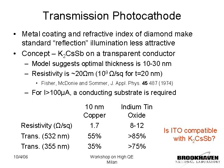
Transmission Photocathode • Metal coating and refractive index of diamond make standard “reflection” illumination less attractive • Concept – K 2 Cs. Sb on a transparent conductor – Model suggests optimal thickness is 10 -30 nm – Resistivity is ~20Ωm (109 Ω/sq for t=20 nm) • Fisher, Mc. Donie and Sommer, J. Appl. Phys. 45 487 (1974) – For I>100μA, a conducting substrate is required 10 nm Copper Indium Tin Oxide Resistivity (Ω/sq) 1. 7 8 -12 Trans. (532 nm) 55% >85% Trans. (355 nm) 35% >75% 10/4/06 Workshop on High QE Milan Is ITO compatible with K 2 Cs. Sb?

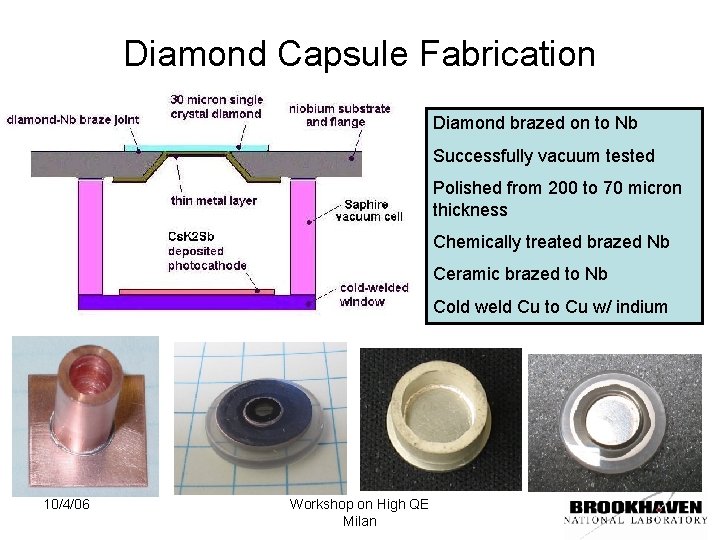
Diamond Capsule Fabrication Diamond brazed on to Nb Successfully vacuum tested Polished from 200 to 70 micron thickness Chemically treated brazed Nb Ceramic brazed to Nb Cold weld Cu to Cu w/ indium 10/4/06 Workshop on High QE Milan

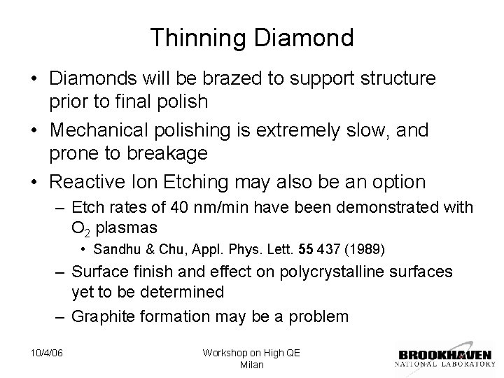
Thinning Diamond • Diamonds will be brazed to support structure prior to final polish • Mechanical polishing is extremely slow, and prone to breakage • Reactive Ion Etching may also be an option – Etch rates of 40 nm/min have been demonstrated with O 2 plasmas • Sandhu & Chu, Appl. Phys. Lett. 55 437 (1989) – Surface finish and effect on polycrystalline surfaces yet to be determined – Graphite formation may be a problem 10/4/06 Workshop on High QE Milan

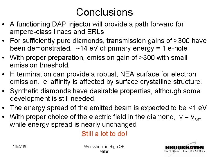
Conclusions • A functioning DAP injector will provide a path forward for ampere-class linacs and ERLs • For sufficiently pure diamonds, transmission gains of >300 have been demonstrated. ~14 e. V of primary energy = 1 e-hole • With proper preparation, emission gain of >300 with small emission threshold. • H termination can provide a robust, NEA surface for electron emission. e- affinity is affected by surface crystalline structure. • Synthetic diamonds have desirable properties, although some development is still needed. • The energy spread of the emitted beam is expected to be <1 e. V • With proper choice of the electric field in the diamond, v = vsat while energy spread is nearly unchanged Still a lot to do! 10/4/06 Workshop on High QE Milan

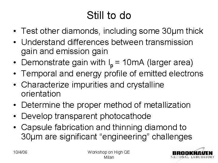
Still to do • Test other diamonds, including some 30μm thick • Understand differences between transmission gain and emission gain • Demonstrate gain with Ip = 10 m. A (larger area) • Temporal and energy profile of emitted electrons • Characterize impurities and crystalline orientation • Determine the proper method of metallization • Develop transparent photocathode • Capsule fabrication and thinning diamond to 30μm are significant “engineering” challenges 10/4/06 Workshop on High QE Milan

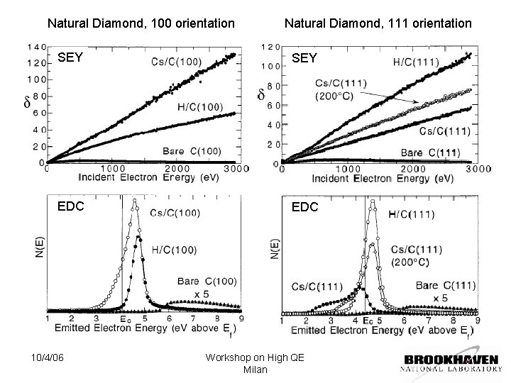
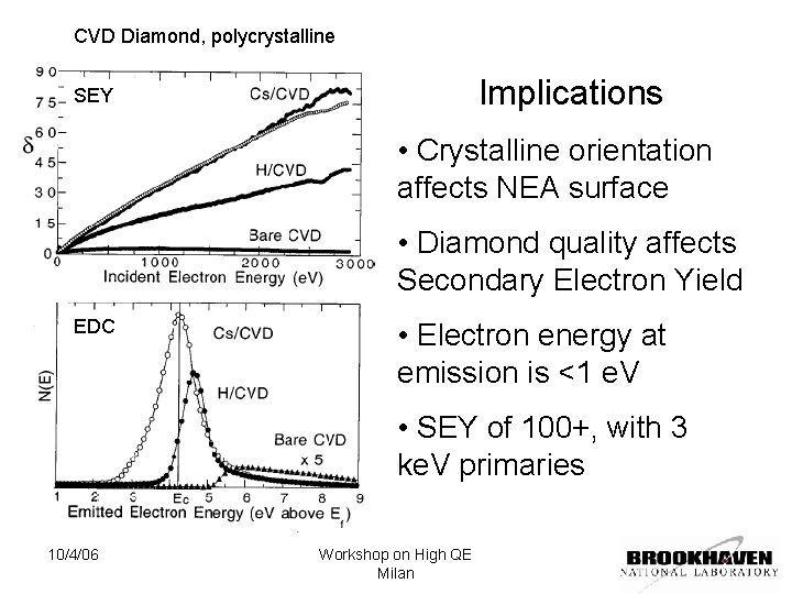
Secondary Electron Yield Measurements • Ongoing work a NRL – J. Yater and A. Shih, J. Applied Physics 87 (2000) 8103, 97 (2005) 093717 • • Primarily reflection mode Boron-doped diamonds, Natural and CVD H or Cs termination Measured Secondary Electron Yield (SEY) and Energy Distribution Curves (EDC) 10/4/06 Workshop on High QE Milan

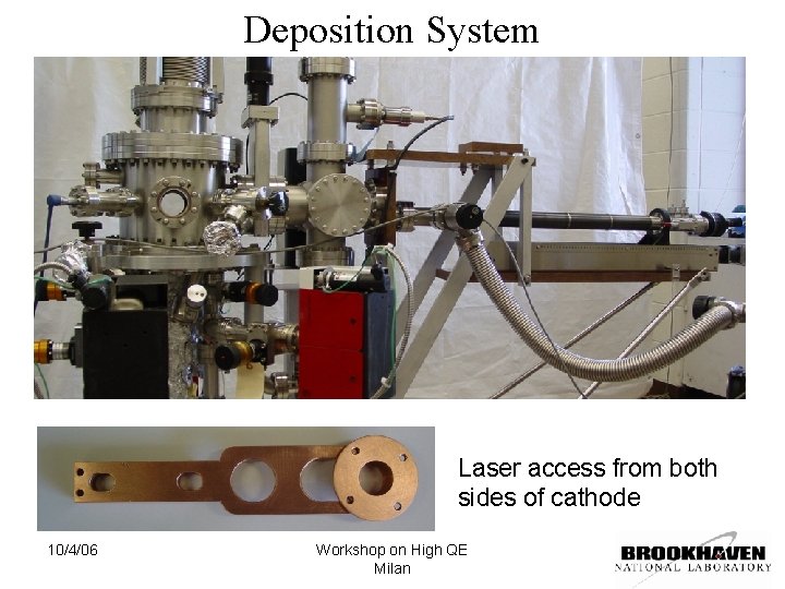
Deposition System Laser access from both sides of cathode 10/4/06 Workshop on High QE Milan

Natural Diamond, 100 orientation Natural Diamond, 111 orientation SEY EDC 10/4/06 Workshop on High QE Milan

CVD Diamond, polycrystalline Implications SEY • Crystalline orientation affects NEA surface • Diamond quality affects Secondary Electron Yield EDC • Electron energy at emission is <1 e. V • SEY of 100+, with 3 ke. V primaries 10/4/06 Workshop on High QE Milan

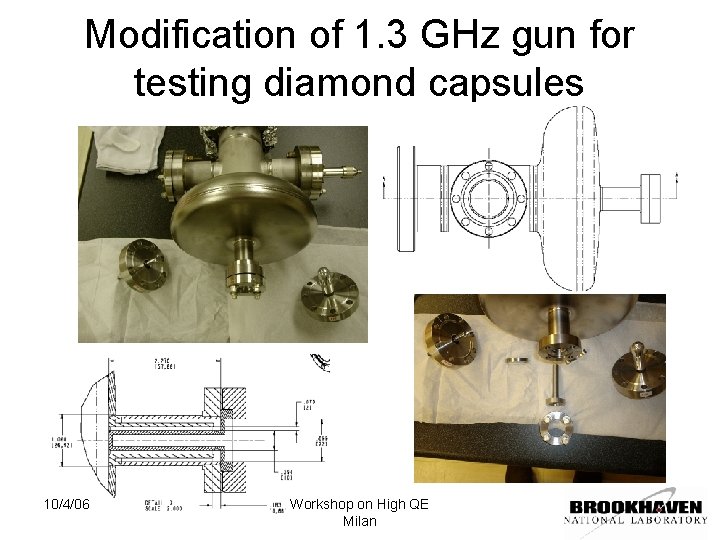
Modification of 1. 3 GHz gun for testing diamond capsules 10/4/06 Workshop on High QE Milan

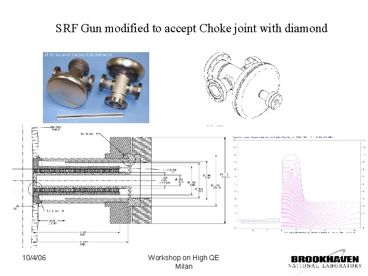
SRF Gun modified to accept Choke joint with diamond 10/4/06 Workshop on High QE Milan

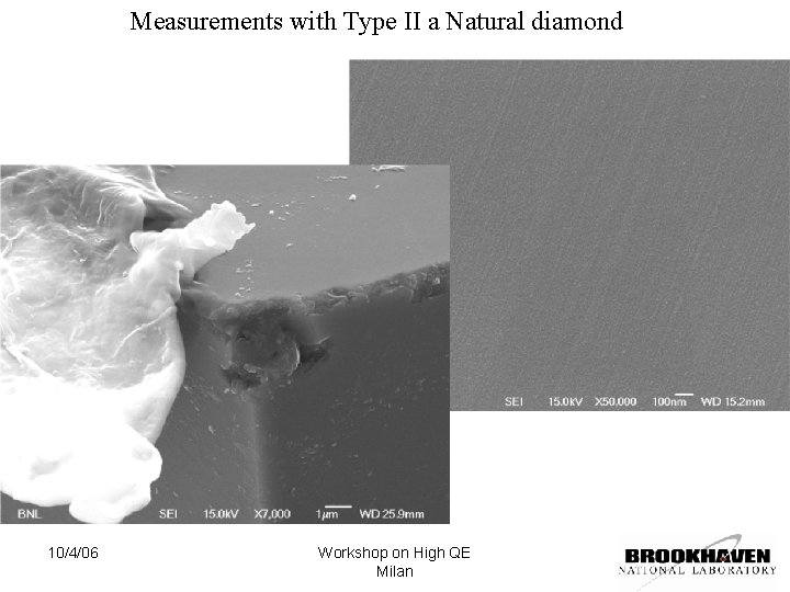
Measurements with Type II a Natural diamond 10/4/06 Workshop on High QE Milan

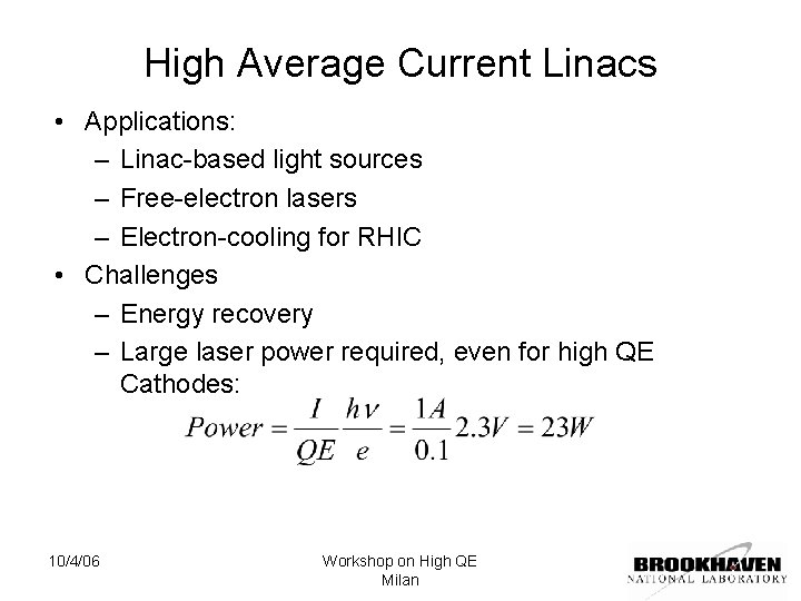
High Average Current Linacs • Applications: – Linac-based light sources – Free-electron lasers – Electron-cooling for RHIC • Challenges – Energy recovery – Large laser power required, even for high QE Cathodes: 10/4/06 Workshop on High QE Milan

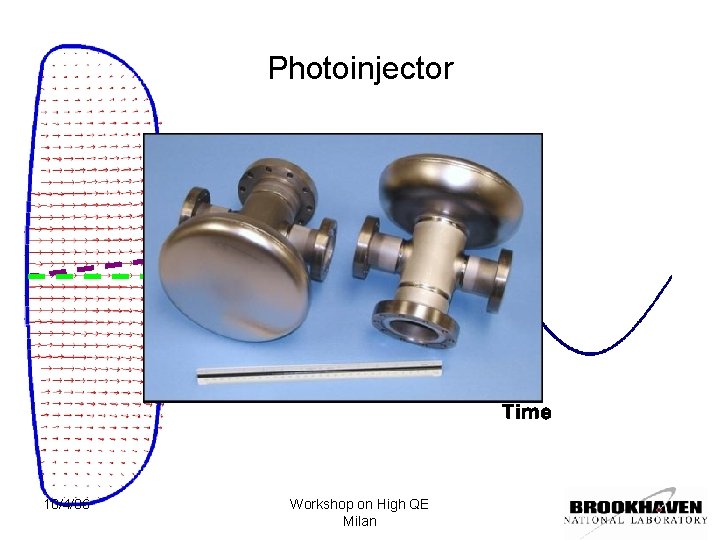
Photoinjector 10/4/06 Workshop on High QE Milan

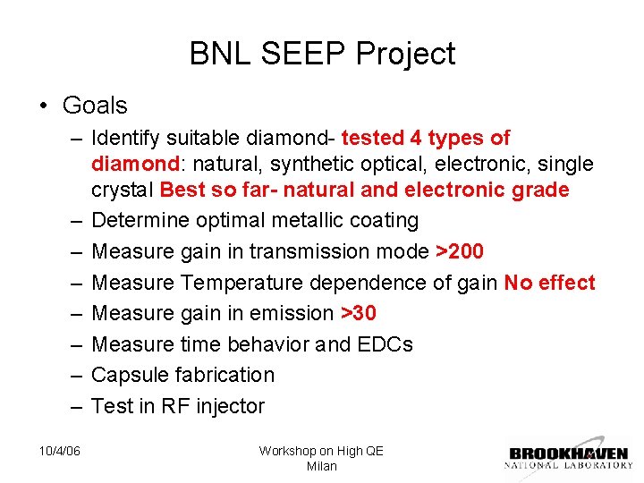
BNL SEEP Project • Goals – Identify suitable diamond- tested 4 types of diamond: natural, synthetic optical, electronic, single crystal Best so far- natural and electronic grade – Determine optimal metallic coating – Measure gain in transmission mode >200 – Measure Temperature dependence of gain No effect – Measure gain in emission >30 – Measure time behavior and EDCs – Capsule fabrication – Test in RF injector 10/4/06 Workshop on High QE Milan