DESIGN OF ELECTRONIC SYSTEMS Course Code 11 EC



- Slides: 82

DESIGN OF ELECTRONIC SYSTEMS Course Code : 11 -EC 201 DEPARTMENT OF ELECTRONICS & COMPUTER ENGINEERING

Diodes Contents • Introduction, • Ideal Diode, • Physical Operation of PN Junction Diode, • Terminal Characteristics of Junction Diodes, • Modeling the Diode Forward Characteristics, • Limiting and Clamping Circuits, • Special Diodes: Operation in the Reverse Breakdown Region in Zener Diodes, The Schottky-Barrier Diode(SBD), Varactors, Photo Diodes, Light Emitting Diodes(LEDS)

Introduction • The diode is the simplest and most fundamental nonlinear circuit element. • Just like resistor, it has two terminals. • Unlike resistor, it has a nonlinear current-voltage characteristics. • Its use in rectifiers is the most common application.

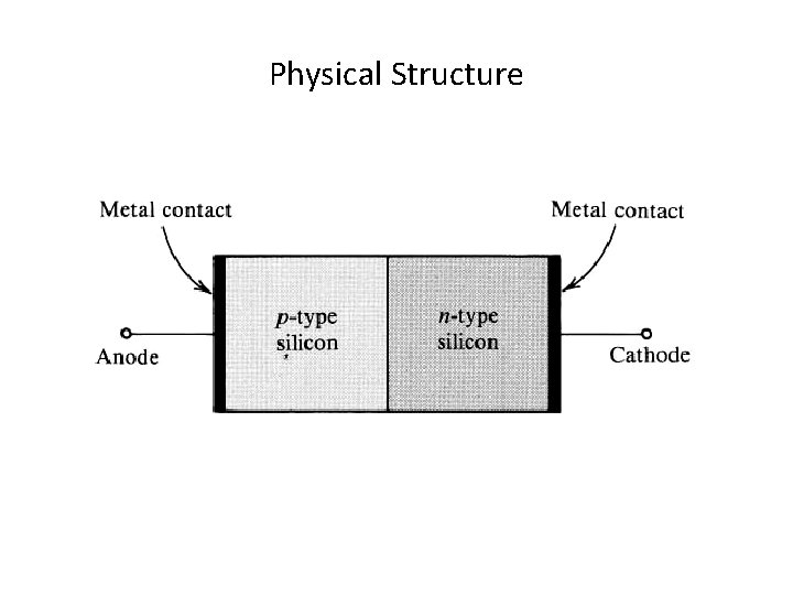
Physical Structure

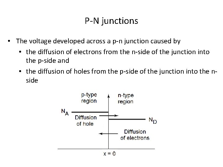
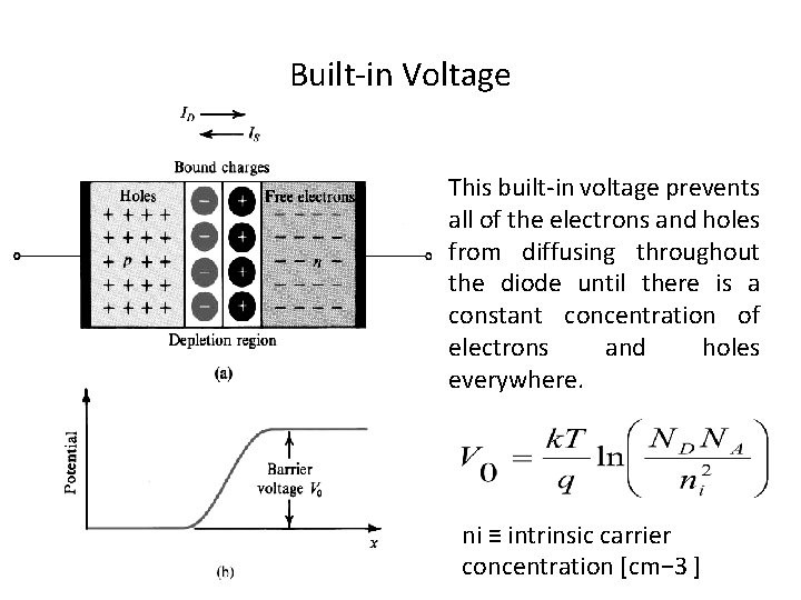
P-N junctions • The voltage developed across a p-n junction caused by • the diffusion of electrons from the n-side of the junction into the p-side and • the diffusion of holes from the p-side of the junction into the nside

Built-in Voltage This built-in voltage prevents all of the electrons and holes from diffusing throughout the diode until there is a constant concentration of electrons and holes everywhere. ni ≡ intrinsic carrier concentration [cm− 3 ]

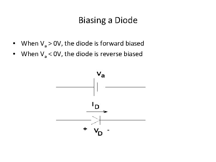
Biasing a Diode • When Va > 0 V, the diode is forward biased • When Va < 0 V, the diode is reverse biased

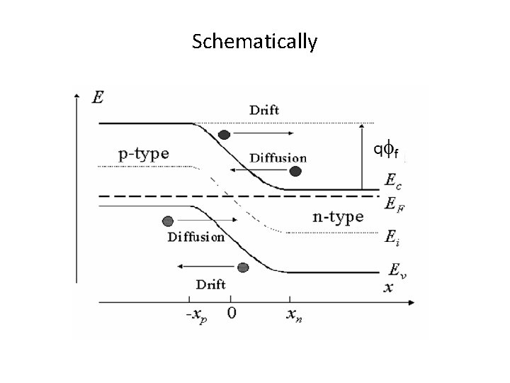
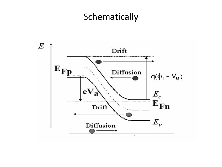
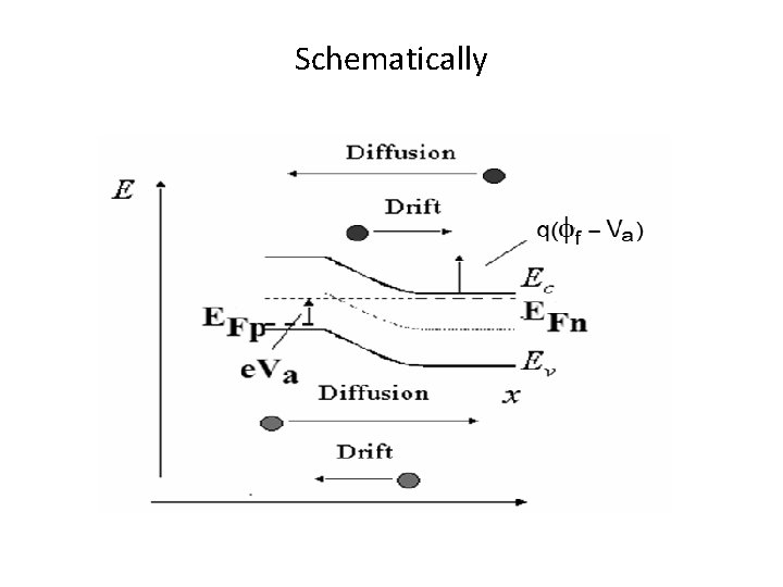
When the applied voltage (Va) is zero • The diode voltage and current are equal to zero on average • Any electron that diffuses through the depletion region from the n-side to the p-side is counterbalanced by an electron that drifts from the p-side to the n-side • Any hole that diffuses through the depletion region from the p-side to the n-side is counterbalanced by an hole that drifts from the n-side to the p-side • So, at any one instant (well under a nanosecond), we may measure a diode current. This current gives rise to one of the sources of electronic noise.

Schematically

When the applied voltage is less than zero • The energy barrier between the p-side and n-side of the diode became larger. • It becomes less favorable for diffusion currents to flow • It become more favorable for drift currents to flow • The diode current is non-zero • The amount of current that flows across the p-n junction depends on the number of electrons in the p-type material and the number of holes in the n-type material • Therefore, the more heavily doped the p-n junction is the smaller the current will be that flows when the diode is reverse biased

Schematically

Applied Voltage is greater than zero • The energy barrier between the p-side and n-side of the diode became smaller with increasing positive applied voltage until there is no barrier left. • It becomes less favorable for drift currents to flow • There is no electric field left to force them to flow • There is nothing to prevent the diffusion currents to flow • The diode current is non-zero • The amount of current that flows across the p-n junction depends on the gradient of electrons (difference in the concentration) between the n- and p-type material and the gradient of holes between the p- and n-type material

When the applied Voltage is greater than zero • The point at which the barrier becomes zero (the flat-band condition) depends on the value of the built-in voltage. The larger the built-in voltage, the more applied voltage is needed to remove the barrier. • It takes more applied voltage to get current to flow for a heavily doped p-n junction

Schematically

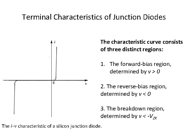
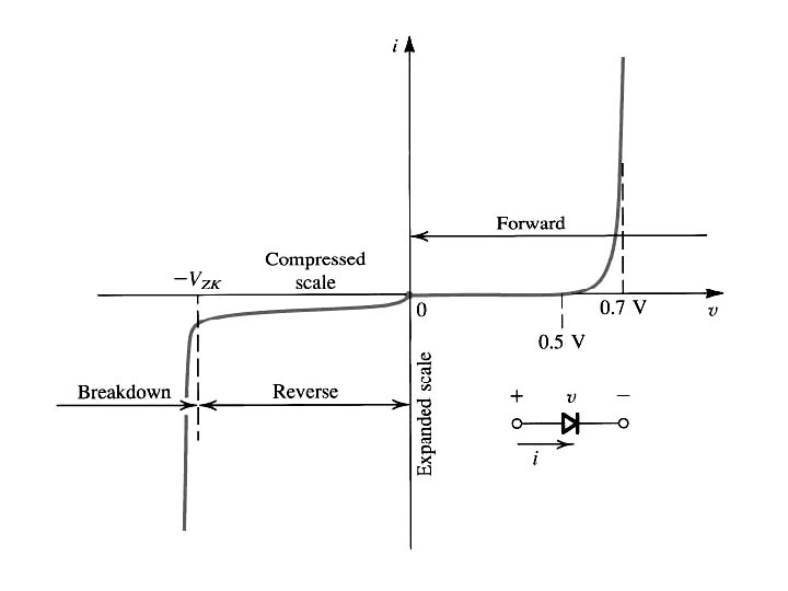
Terminal Characteristics of Junction Diodes The characteristic curve consists of three distinct regions: 1. The forward-bias region, determined by v > 0 2. The reverse-bias region, determined by v < 0 3. The breakdown region, determined by v < -VZK The i–v characteristic of a silicon junction diode.

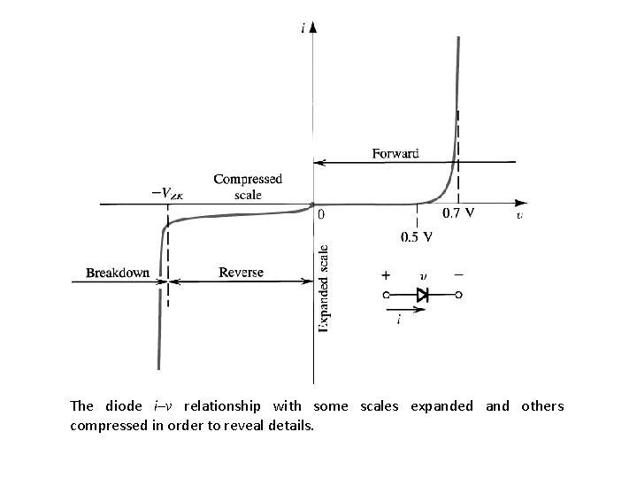
The diode i–v relationship with some scales expanded and others compressed in order to reveal details.

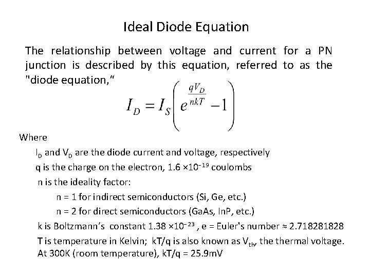
Ideal Diode Equation The relationship between voltage and current for a PN junction is described by this equation, referred to as the "diode equation, “ Where ID and VD are the diode current and voltage, respectively q is the charge on the electron, 1. 6 × 10− 19 coulombs n is the ideality factor: n = 1 for indirect semiconductors (Si, Ge, etc. ) n = 2 for direct semiconductors (Ga. As, In. P, etc. ) k is Boltzmann’s constant 1. 38 × 10− 23 , e = Euler's number ≈ 2. 71828 T is temperature in Kelvin; k. T/q is also known as Vth, thermal voltage. At 300 K (room temperature), k. T/q = 25. 9 m. V

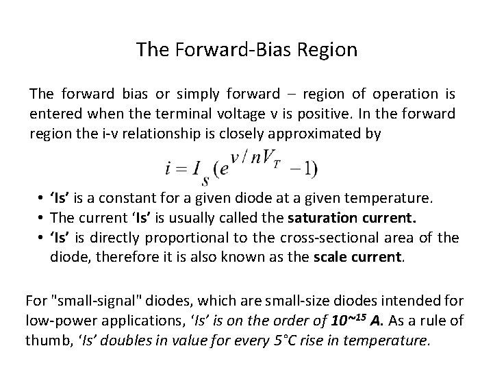
The Forward-Bias Region The forward bias or simply forward – region of operation is entered when the terminal voltage v is positive. In the forward region the i-v relationship is closely approximated by • ‘Is’ is a constant for a given diode at a given temperature. • The current ‘Is’ is usually called the saturation current. • ‘Is’ is directly proportional to the cross-sectional area of the diode, therefore it is also known as the scale current. For "small-signal" diodes, which are small-size diodes intended for low-power applications, ‘Is’ is on the order of 10~15 A. As a rule of thumb, ‘Is’ doubles in value for every 5°C rise in temperature.

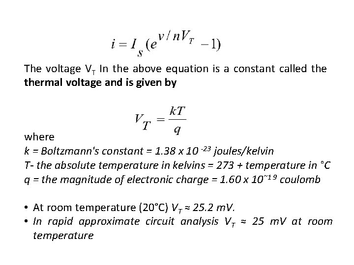
The voltage VT In the above equation is a constant called thermal voltage and is given by where k = Boltzmann's constant = 1. 38 x 10 -23 joules/kelvin T- the absolute temperature in kelvins = 273 + temperature in °C q = the magnitude of electronic charge = 1. 60 x 10~1 9 coulomb • At room temperature (20°C) VT ≈ 25. 2 m. V. • In rapid approximate circuit analysis VT ≈ 25 m. V at room temperature

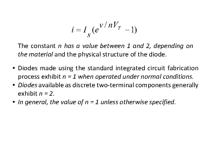
The constant n has a value between 1 and 2, depending on the material and the physical structure of the diode. • Diodes made using the standard integrated circuit fabrication process exhibit n = 1 when operated under normal conditions. • Diodes available as discrete two-terminal components generally exhibit n = 2. • In general, the value of n = 1 unless otherwise specified.

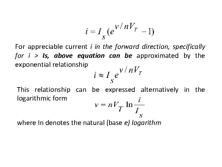
For appreciable current i in the forward direction, specifically for i > Is, above equation can be approximated by the exponential relationship This relationship can be expressed alternatively in the logarithmic form where In denotes the natural (base e) logarithm

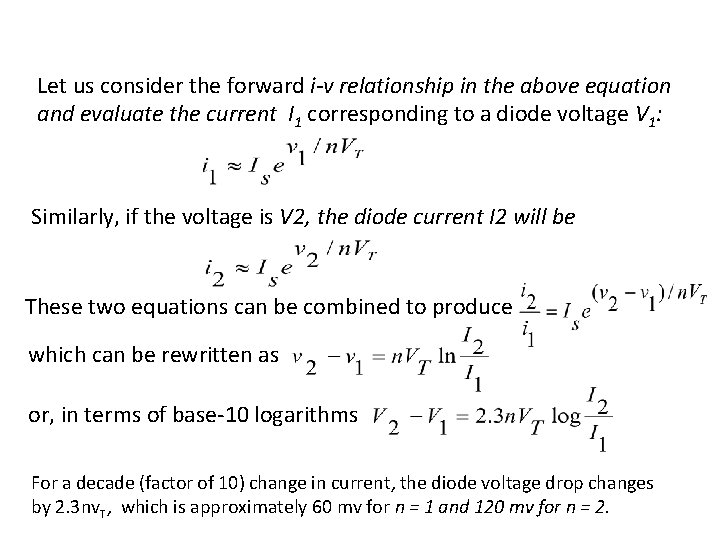
Let us consider the forward i-v relationship in the above equation and evaluate the current I 1 corresponding to a diode voltage V 1: Similarly, if the voltage is V 2, the diode current I 2 will be These two equations can be combined to produce which can be rewritten as or, in terms of base-10 logarithms For a decade (factor of 10) change in current, the diode voltage drop changes by 2. 3 nv. T, which is approximately 60 mv for n = 1 and 120 mv for n = 2.

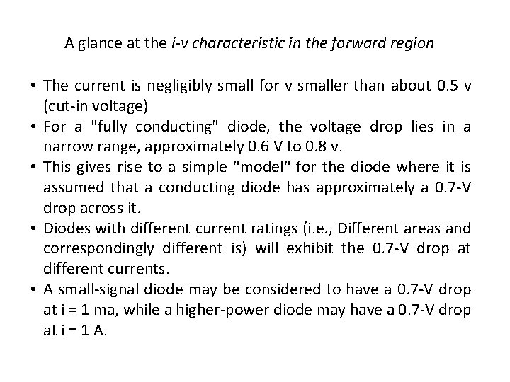
A glance at the i-v characteristic in the forward region • The current is negligibly small for v smaller than about 0. 5 v (cut-in voltage) • For a "fully conducting" diode, the voltage drop lies in a narrow range, approximately 0. 6 V to 0. 8 v. • This gives rise to a simple "model" for the diode where it is assumed that a conducting diode has approximately a 0. 7 -V drop across it. • Diodes with different current ratings (i. e. , Different areas and correspondingly different is) will exhibit the 0. 7 -V drop at different currents. • A small-signal diode may be considered to have a 0. 7 -V drop at i = 1 ma, while a higher-power diode may have a 0. 7 -V drop at i = 1 A.

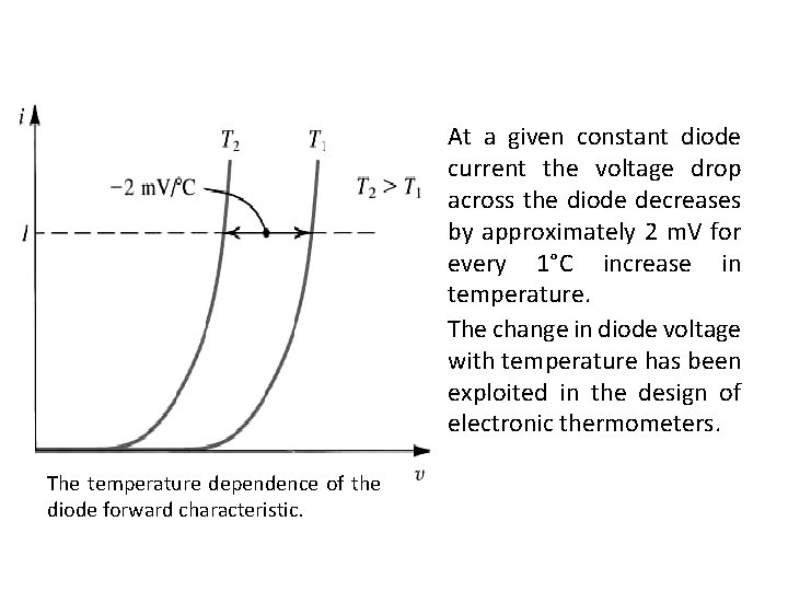
At a given constant diode current the voltage drop across the diode decreases by approximately 2 m. V for every 1°C increase in temperature. The change in diode voltage with temperature has been exploited in the design of electronic thermometers. The temperature dependence of the diode forward characteristic.

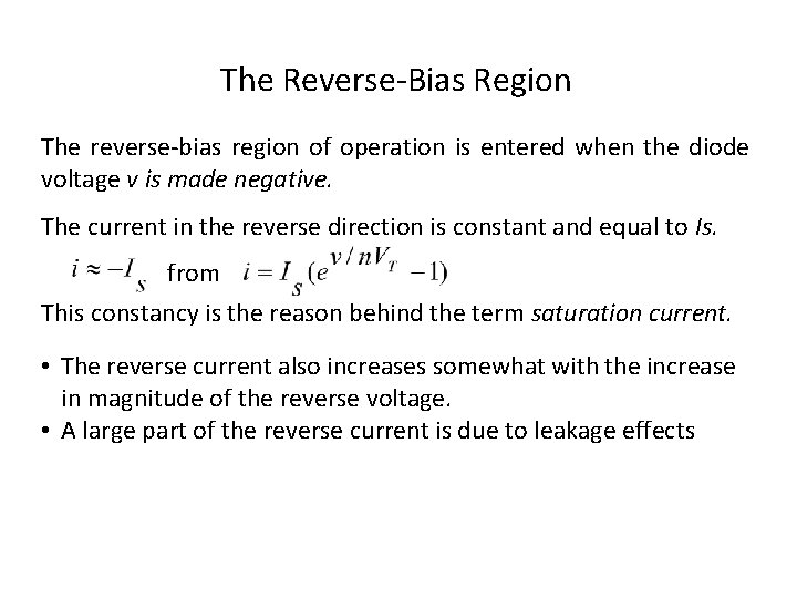
The Reverse-Bias Region The reverse-bias region of operation is entered when the diode voltage v is made negative. The current in the reverse direction is constant and equal to Is. from This constancy is the reason behind the term saturation current. • The reverse current also increases somewhat with the increase in magnitude of the reverse voltage. • A large part of the reverse current is due to leakage effects


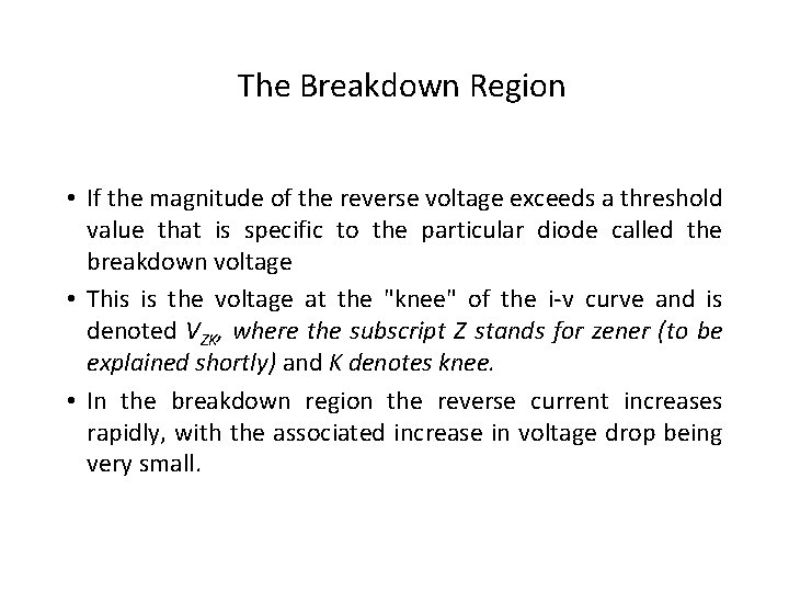
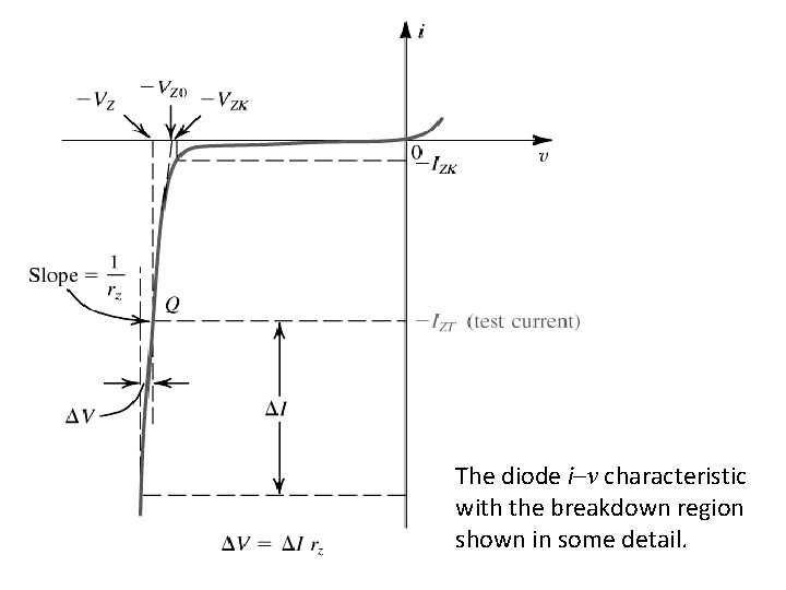
The Breakdown Region • If the magnitude of the reverse voltage exceeds a threshold value that is specific to the particular diode called the breakdown voltage • This is the voltage at the "knee" of the i-v curve and is denoted VZK, where the subscript Z stands for zener (to be explained shortly) and K denotes knee. • In the breakdown region the reverse current increases rapidly, with the associated increase in voltage drop being very small.

EXAMPLE

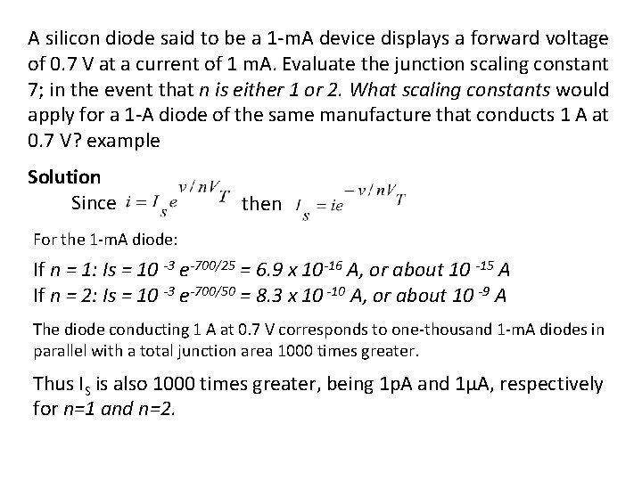
A silicon diode said to be a 1 -m. A device displays a forward voltage of 0. 7 V at a current of 1 m. A. Evaluate the junction scaling constant 7; in the event that n is either 1 or 2. What scaling constants would apply for a 1 -A diode of the same manufacture that conducts 1 A at 0. 7 V? example Solution Since then For the 1 -m. A diode: If n = 1: Is = 10 -3 e-700/25 = 6. 9 x 10 -16 A, or about 10 -15 A If n = 2: Is = 10 -3 e-700/50 = 8. 3 x 10 -10 A, or about 10 -9 A The diode conducting 1 A at 0. 7 V corresponds to one-thousand 1 -m. A diodes in parallel with a total junction area 1000 times greater. Thus IS is also 1000 times greater, being 1 p. A and 1µA, respectively for n=1 and n=2.

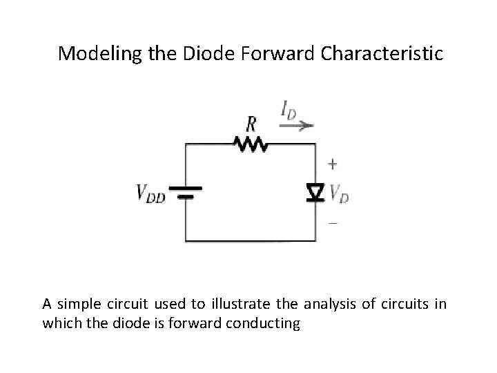
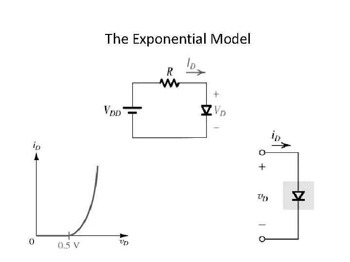
Modeling the Diode Forward Characteristic A simple circuit used to illustrate the analysis of circuits in which the diode is forward conducting

The Exponential Model

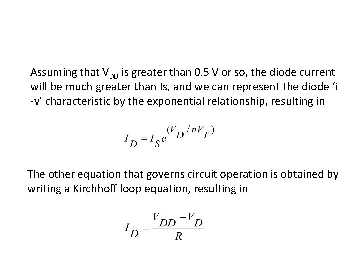
Assuming that VDD is greater than 0. 5 V or so, the diode current will be much greater than Is, and we can represent the diode ‘i -v’ characteristic by the exponential relationship, resulting in The other equation that governs circuit operation is obtained by writing a Kirchhoff loop equation, resulting in

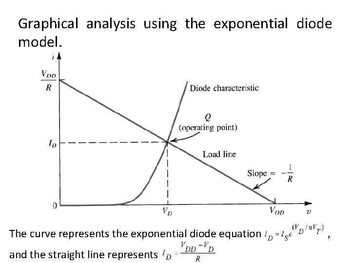
Graphical analysis using the exponential diode model. The curve represents the exponential diode equation and the straight line represents ,

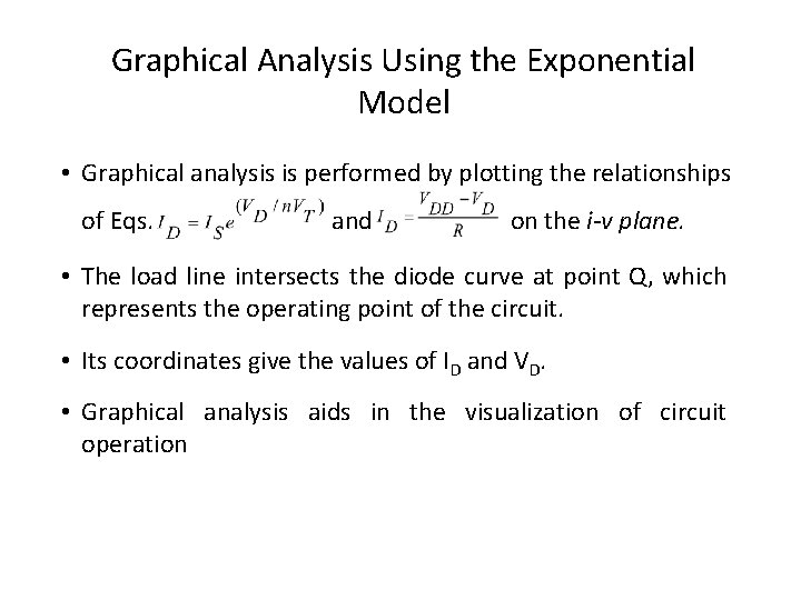
Graphical Analysis Using the Exponential Model • Graphical analysis is performed by plotting the relationships of Eqs. and on the i-v plane. • The load line intersects the diode curve at point Q, which represents the operating point of the circuit. • Its coordinates give the values of ID and VD. • Graphical analysis aids in the visualization of circuit operation

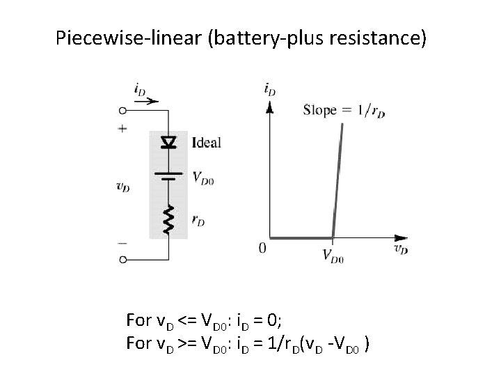
Piecewise-linear (battery-plus resistance) For v. D <= VD 0: i. D = 0; For v. D >= VD 0: i. D = 1/r. D(v. D -VD 0 )

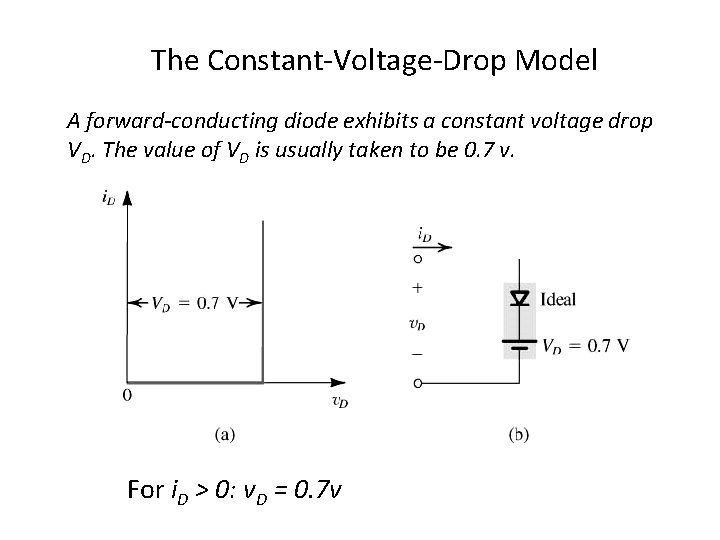
The Constant-Voltage-Drop Model A forward-conducting diode exhibits a constant voltage drop VD. The value of VD is usually taken to be 0. 7 v. For i. D > 0: v. D = 0. 7 v

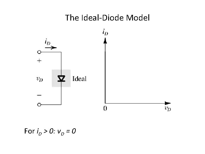
The Ideal-Diode Model For i. D > 0: v. D = 0

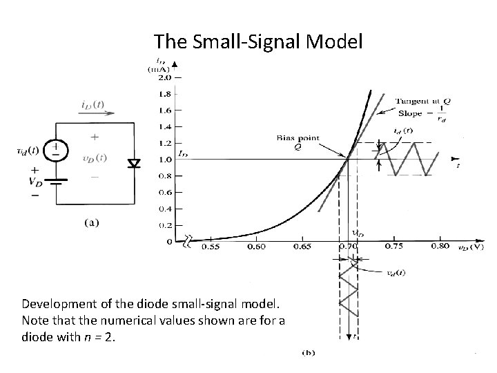
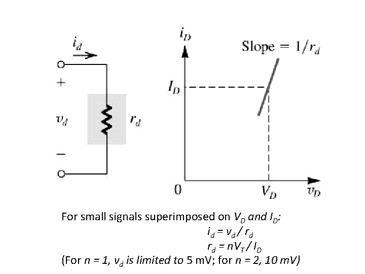
The Small-Signal Model Development of the diode small-signal model. Note that the numerical values shown are for a diode with n = 2.

For small signals superimposed on VD and ID: id = v d / r d rd = n. VT / ID (For n = 1, vd is limited to 5 m. V; for n = 2, 10 m. V)

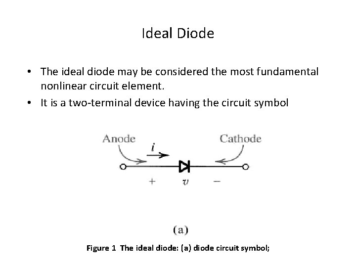
Ideal Diode • The ideal diode may be considered the most fundamental nonlinear circuit element. • It is a two-terminal device having the circuit symbol Figure 1 The ideal diode: (a) diode circuit symbol;

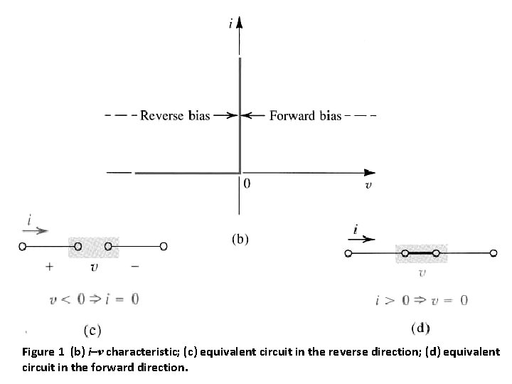
Figure 1 (b) i–v characteristic; (c) equivalent circuit in the reverse direction; (d) equivalent circuit in the forward direction.

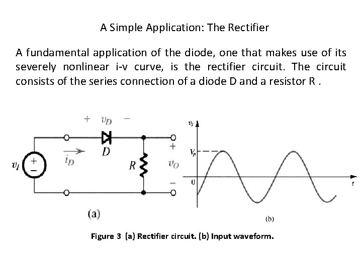
A Simple Application: The Rectifier A fundamental application of the diode, one that makes use of its severely nonlinear i-v curve, is the rectifier circuit. The circuit consists of the series connection of a diode D and a resistor R. Figure 3 (a) Rectifier circuit. (b) Input waveform.

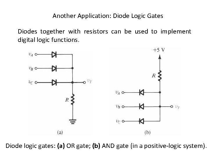
Another Application: Diode Logic Gates Diodes together with resistors can be used to implement digital logic functions. Diode logic gates: (a) OR gate; (b) AND gate (in a positive-logic system).

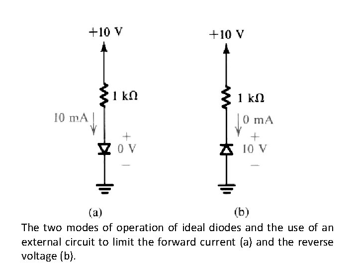
The two modes of operation of ideal diodes and the use of an external circuit to limit the forward current (a) and the reverse voltage (b).

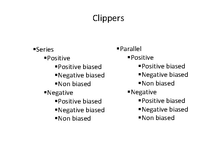
Clippers §Series §Positive biased §Negative biased §Non biased §Negative §Positive biased §Negative biased §Non biased §Parallel §Positive biased §Negative biased §Non biased §Negative §Positive biased §Negative biased §Non biased

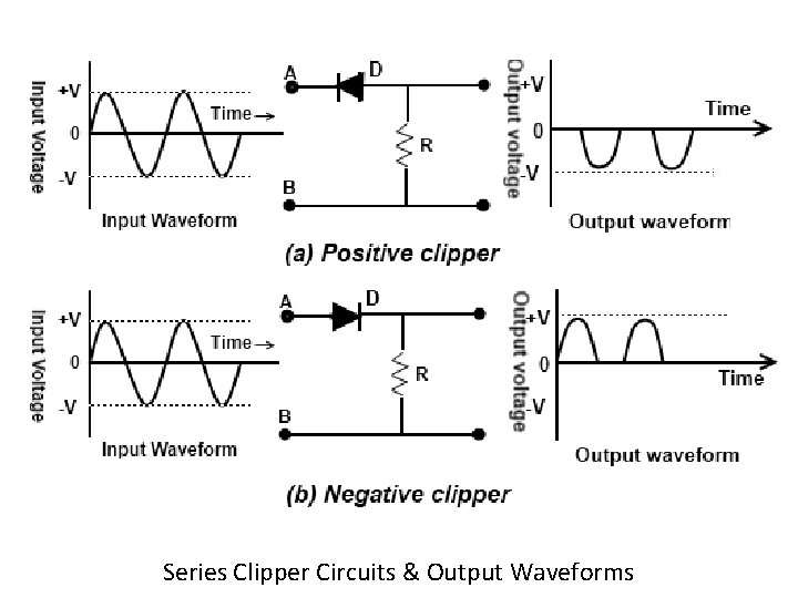
Series Clipper Circuits & Output Waveforms

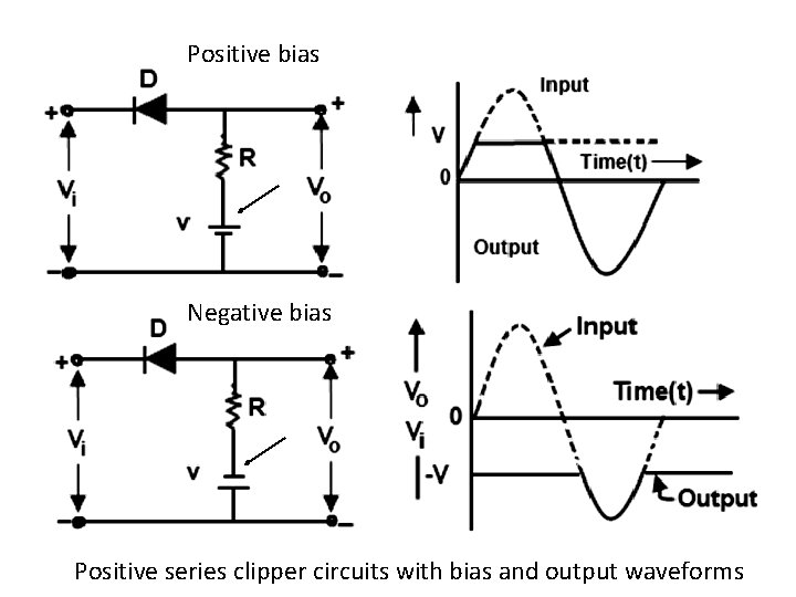
Positive bias Negative bias Positive series clipper circuits with bias and output waveforms

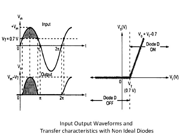
Input Output Waveforms and Transfer characteristics with Non Ideal Diodes

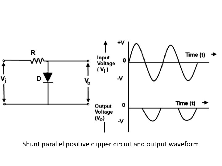
Shunt parallel positive clipper circuit and output waveform

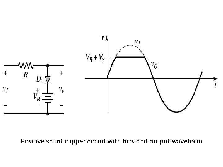
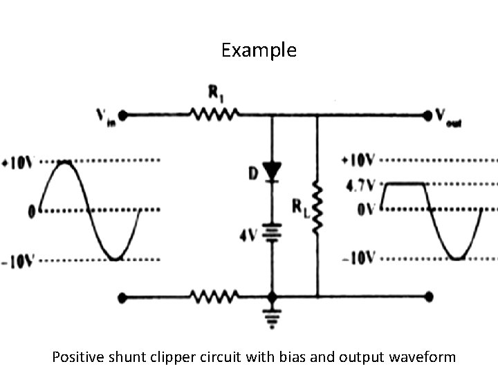
Positive shunt clipper circuit with bias and output waveform

Example Positive shunt clipper circuit with bias and output waveform

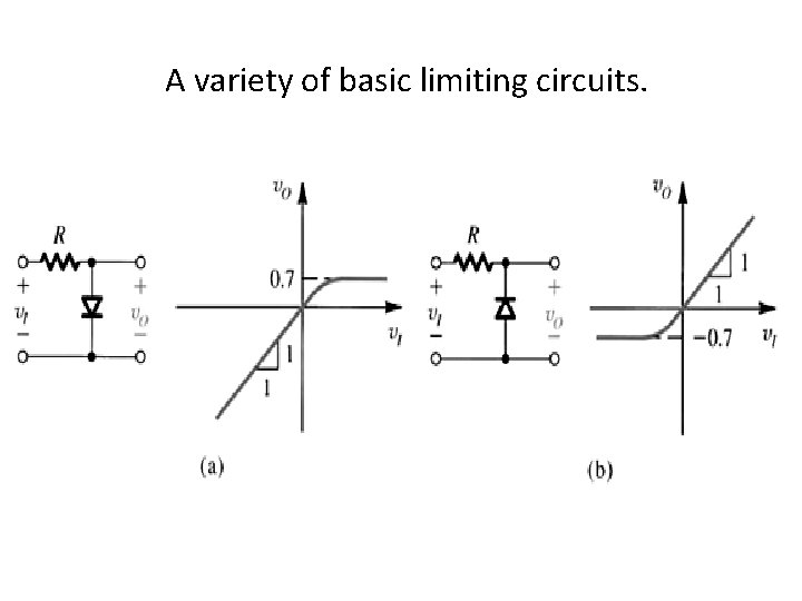
A variety of basic limiting circuits.

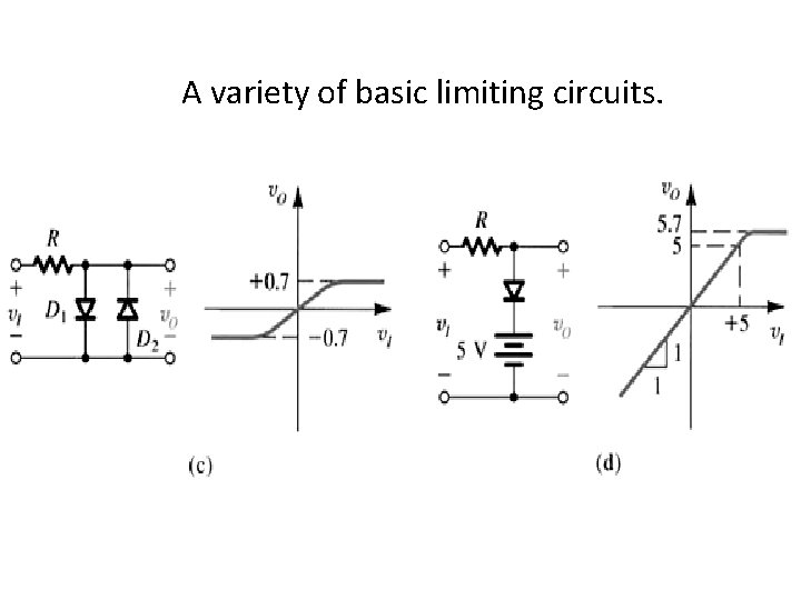
A variety of basic limiting circuits.

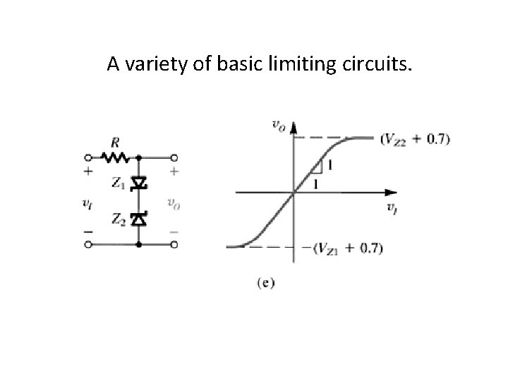
A variety of basic limiting circuits.

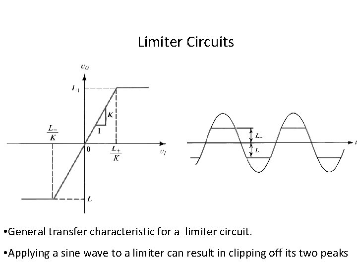
Limiter Circuits • General transfer characteristic for a limiter circuit. • Applying a sine wave to a limiter can result in clipping off its two peaks

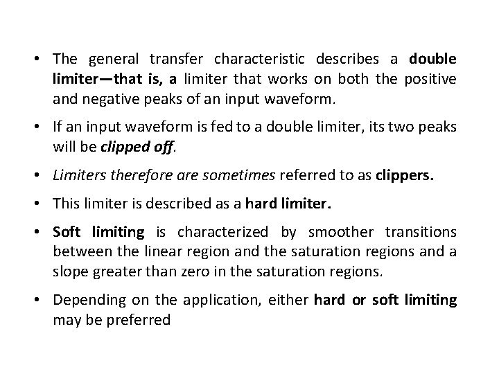
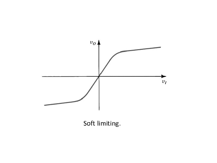
• The general transfer characteristic describes a double limiter—that is, a limiter that works on both the positive and negative peaks of an input waveform. • If an input waveform is fed to a double limiter, its two peaks will be clipped off. • Limiters therefore are sometimes referred to as clippers. • This limiter is described as a hard limiter. • Soft limiting is characterized by smoother transitions between the linear region and the saturation regions and a slope greater than zero in the saturation regions. • Depending on the application, either hard or soft limiting may be preferred

Soft limiting.

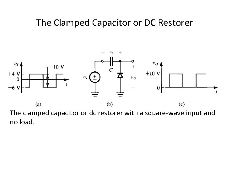
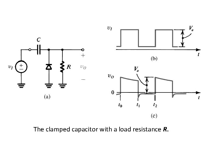
The Clamped Capacitor or DC Restorer The clamped capacitor or dc restorer with a square-wave input and no load.

• The output waveform will therefore have its lowest peak clamped to 0 V, which is why the circuit is called a clamped capacitor. • Feeding the resulting pulse waveform to a clamping circuit provides it with a well-determined dc component, a process known as dc restoration. Therefore This circuit is also called a dc restorer

The clamped capacitor with a load resistance R.

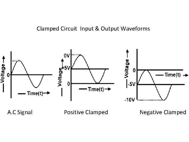
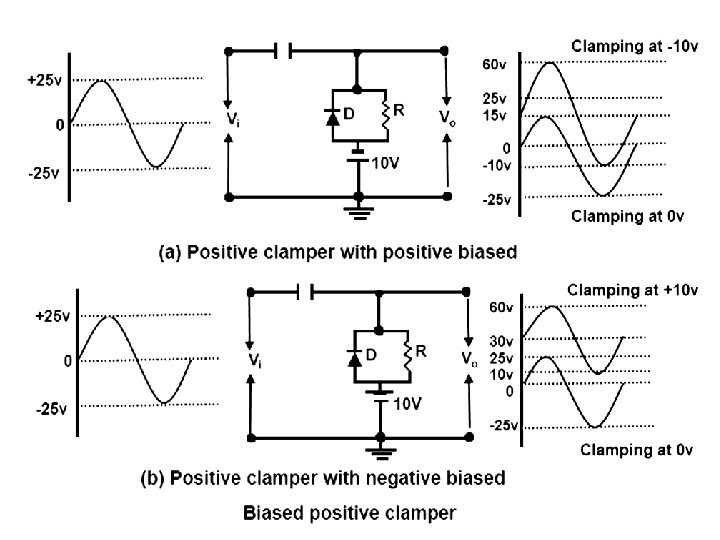
Clamped Circuit Input & Output Waveforms A. C Signal Positive Clamped Negative Clamped


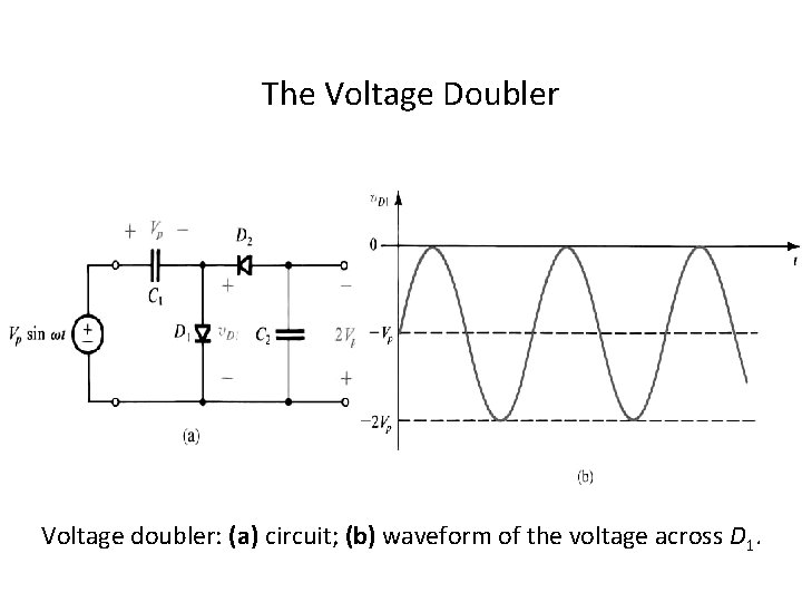
The Voltage Doubler Voltage doubler: (a) circuit; (b) waveform of the voltage across D 1.

Types of diodes • Rectifier diodes are typically used for power supply applications. Within the power supply, you will see diodes as elements that convert AC power to DC power. • Switching diodes have lower power ratings than rectifier diodes, but can function better in high frequency application and in clipping and clamping operations that deal with short-duration pulse waveforms

Types of diodes • Zener diodes, a special kind of diode that can recover from breakdown caused when the reverse-bias voltage exceeds the diode breakdown voltage. These diodes are commonly used as voltage-level regulators and protectors against high voltage surges • Optical diodes • Special diodes, such as varactors (diodes with variable capacity), tunnel diodes or Schottky diodes

Types of diodes • Zener diodes, a special kind of diode that can recover from breakdown caused when the reverse-bias voltage exceeds the diode breakdown voltage. These diodes are commonly used as voltage-level regulators and protectors against high voltage surges • Optical diodes • Special diodes, such as varactors (diodes with variable capacity), tunnel diodes or Schottky diodes

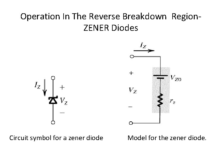
Operation In The Reverse Breakdown Region. ZENER Diodes Circuit symbol for a zener diode Model for the zener diode.

The diode i–v characteristic with the breakdown region shown in some detail.

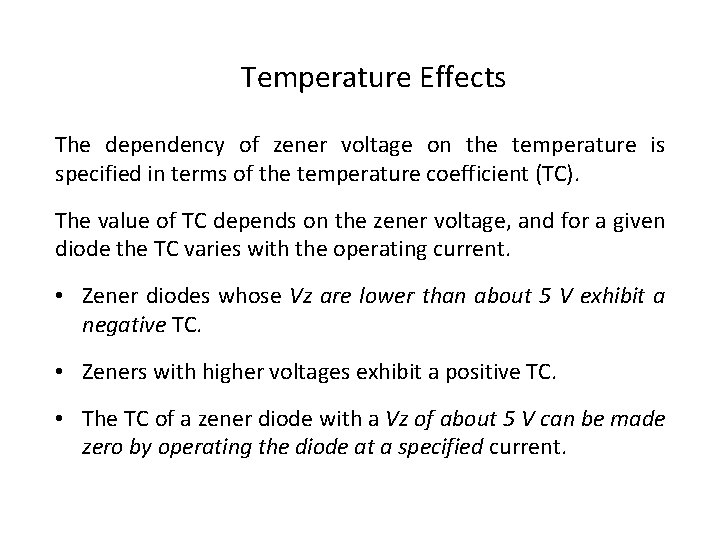
Temperature Effects The dependency of zener voltage on the temperature is specified in terms of the temperature coefficient (TC). The value of TC depends on the zener voltage, and for a given diode the TC varies with the operating current. • Zener diodes whose Vz are lower than about 5 V exhibit a negative TC. • Zeners with higher voltages exhibit a positive TC. • The TC of a zener diode with a Vz of about 5 V can be made zero by operating the diode at a specified current.

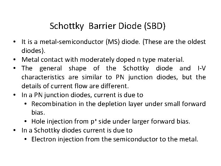
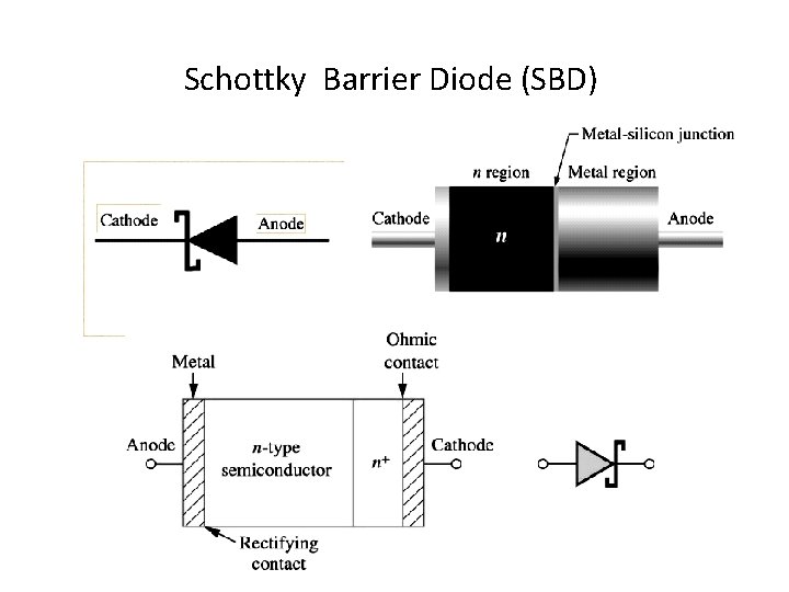
Schottky Barrier Diode (SBD) • It is a metal-semiconductor (MS) diode. (These are the oldest diodes). • Metal contact with moderately doped n type material. • The general shape of the Schottky diode and I-V characteristics are similar to PN junction diodes, but the details of current flow are different. • In a PN junction diodes, current is due to • Recombination in the depletion layer under small forward bias. • Hole injection from p+ side under larger forward bias. • In a Schottky diodes current is due to • Electron injection from the semiconductor to the metal.

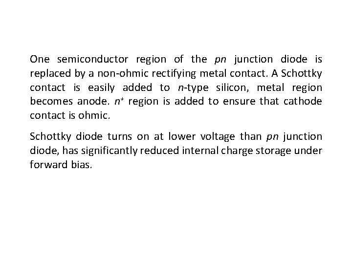
One semiconductor region of the pn junction diode is replaced by a non-ohmic rectifying metal contact. A Schottky contact is easily added to n-type silicon, metal region becomes anode. n+ region is added to ensure that cathode contact is ohmic. Schottky diode turns on at lower voltage than pn junction diode, has significantly reduced internal charge storage under forward bias.

Schottky Barrier Diode (SBD)

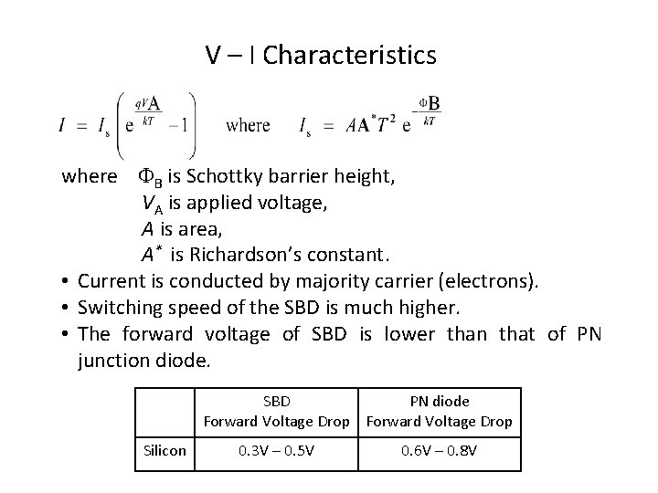
V – I Characteristics where B is Schottky barrier height, VA is applied voltage, A is area, A* is Richardson’s constant. • Current is conducted by majority carrier (electrons). • Switching speed of the SBD is much higher. • The forward voltage of SBD is lower than that of PN junction diode. SBD PN diode Forward Voltage Drop Silicon 0. 3 V – 0. 5 V 0. 6 V – 0. 8 V

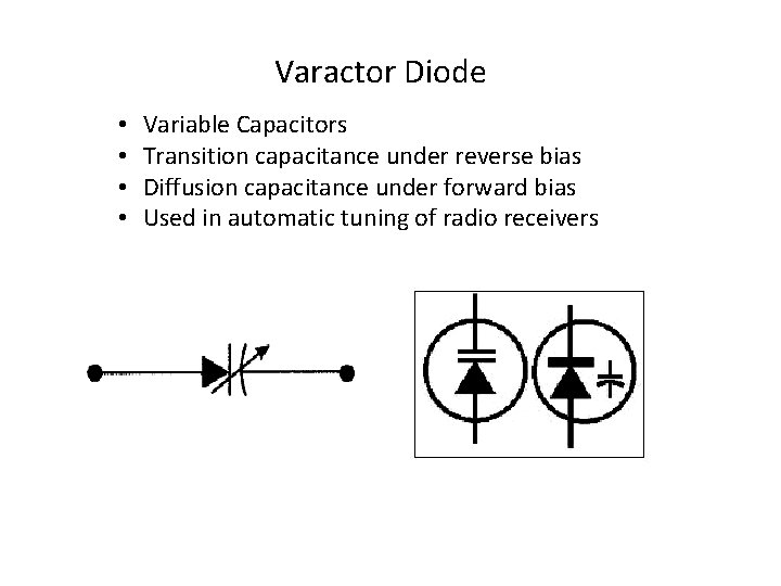
Varactor Diode • • Variable Capacitors Transition capacitance under reverse bias Diffusion capacitance under forward bias Used in automatic tuning of radio receivers

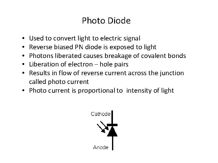
Photo Diode Used to convert light to electric signal Reverse biased PN diode is exposed to light Photons liberated causes breakage of covalent bonds Liberation of electron – hole pairs Results in flow of reverse current across the junction called photo current • Photo current is proportional to intensity of light • • •

Light Emitting Diode (LED) • The operation is inverse to that of a photo diode • It converts forward current in to light • Minority carriers are injected across the junction and diffuse in to P & N regions • Minority carriers recombine with majority carriers emitting photons • Made of types III-V semiconductors (e. g. , Ga. As). • Use direct band gap materials like Gallium Arsenide • Light emitted proportional to the no. of re-combinations • Wide range of applications in different types of displays • In order to have a visible light output, the band gap of the semiconductor should be larger then Si. • Have a much larger VD 0 between 1. 7 to 1. 9 V.

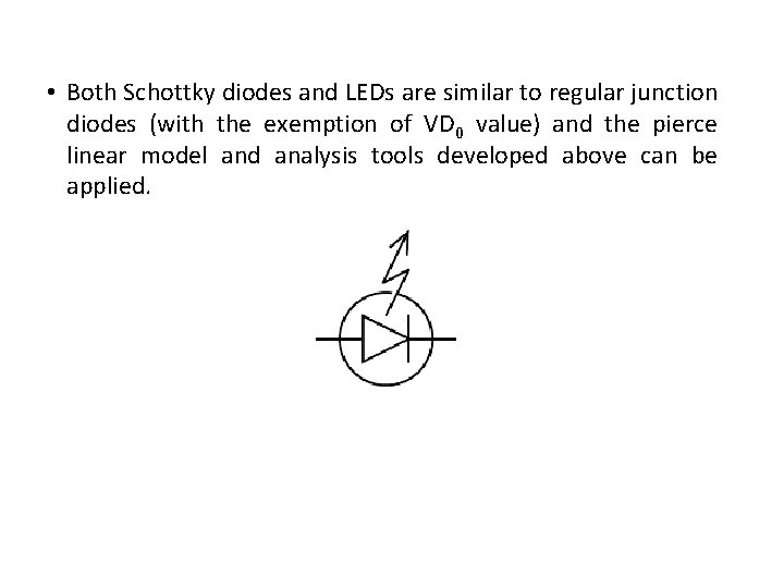
• Both Schottky diodes and LEDs are similar to regular junction diodes (with the exemption of VD 0 value) and the pierce linear model and analysis tools developed above can be applied.

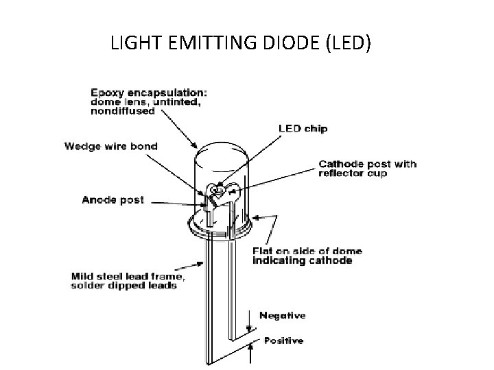
LIGHT EMITTING DIODE (LED)

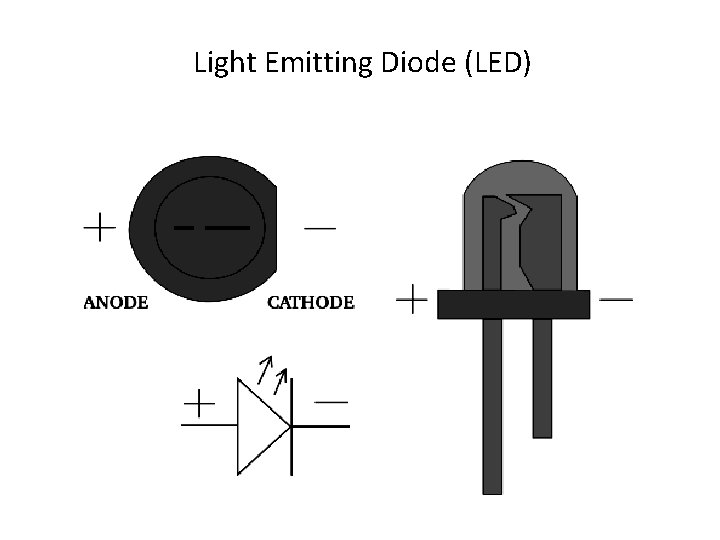
Light Emitting Diode (LED)

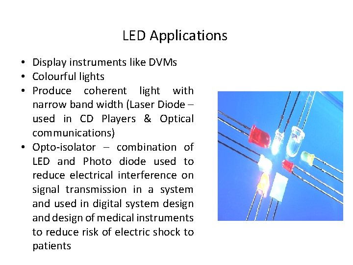
LED Applications • Display instruments like DVMs • Colourful lights • Produce coherent light with narrow band width (Laser Diode – used in CD Players & Optical communications) • Opto-isolator – combination of LED and Photo diode used to reduce electrical interference on signal transmission in a system and used in digital system design and design of medical instruments to reduce risk of electric shock to patients

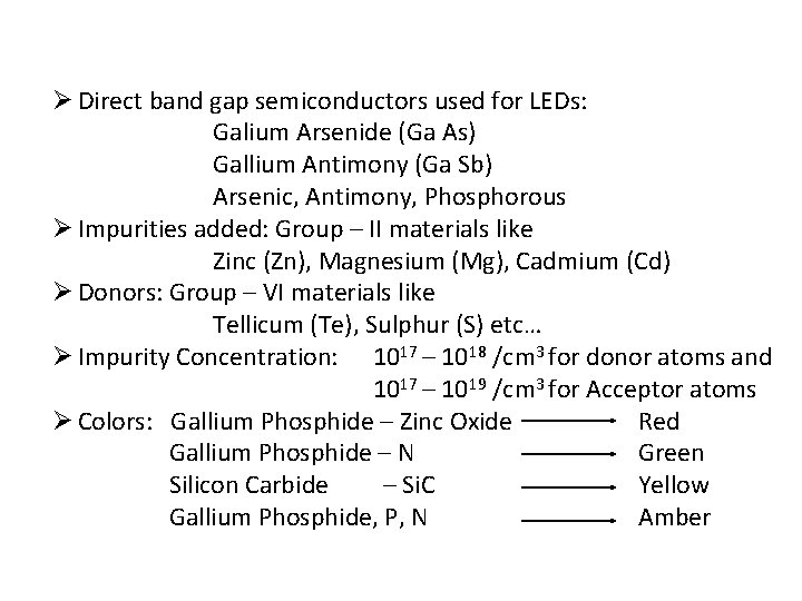
Ø Direct band gap semiconductors used for LEDs: Galium Arsenide (Ga As) Gallium Antimony (Ga Sb) Arsenic, Antimony, Phosphorous Ø Impurities added: Group – II materials like Zinc (Zn), Magnesium (Mg), Cadmium (Cd) Ø Donors: Group – VI materials like Tellicum (Te), Sulphur (S) etc… Ø Impurity Concentration: 1017 – 1018 /cm 3 for donor atoms and 1017 – 1019 /cm 3 for Acceptor atoms Ø Colors: Gallium Phosphide – Zinc Oxide Red Gallium Phosphide – N Green Silicon Carbide – Si. C Yellow Gallium Phosphide, P, N Amber

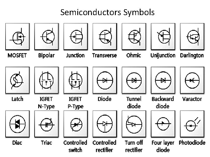
Semiconductors Symbols