CSE 140 Discussion Section Midterm 2 Review Mingjing
- Slides: 16

CSE 140 Discussion Section Midterm #2 Review Mingjing Chen

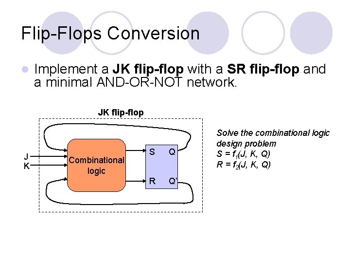
Flip-Flops Conversion l Implement a JK flip-flop with a SR flip-flop and a minimal AND-OR-NOT network. JK flip-flop J K Combinational logic S Q R Q’ Solve the combinational logic design problem S = f 1(J, K, Q) R = f 2(J, K, Q)

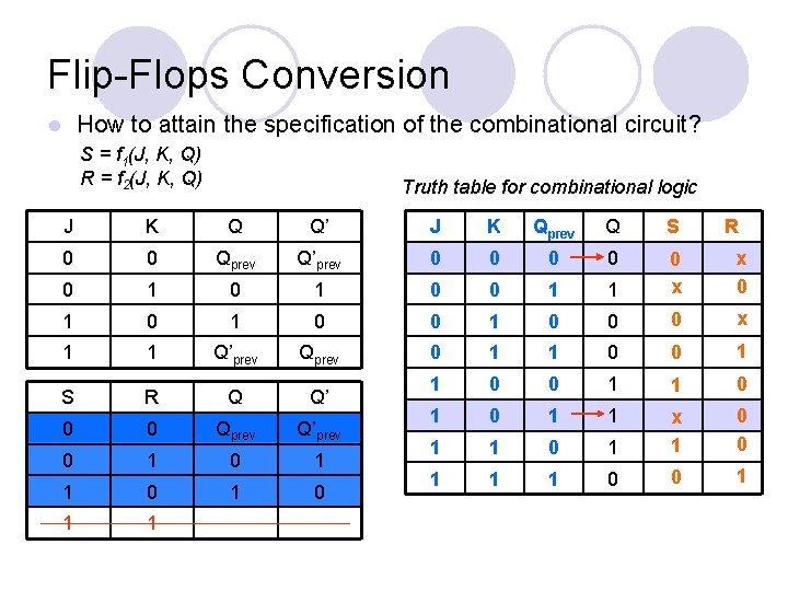
Flip-Flops Conversion How to attain the specification of the combinational circuit? l S = f 1(J, K, Q) R = f 2(J, K, Q) Truth table for combinational logic J K Q Q’ J K Qprev Q S R 0 0 Qprev Q’prev 0 0 0 1 1 0 x x 0 1 0 0 0 x 1 1 Q’prev Qprev 0 1 1 0 0 1 S R Q Q’ 1 0 0 1 1 0 0 0 Qprev Q’prev 1 0 1 0 1 1 1 0 1 x 1 0 0 1 0 1 1 1 0 0 1 1 1

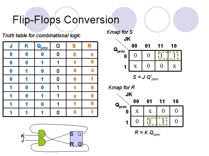
Flip-Flops Conversion Truth table for combinational logic J K Qprev Q S R 0 0 0 1 1 0 x x 0 0 1 0 0 0 x 0 1 1 0 1 1 0 1 x 1 0 0 1 1 1 0 0 1 Kmap for S JK 00 Qprev 0 0 01 11 10 0 1 1 x 0 0 x 1 S = J Q’prev Kmap for R JK 00 Qprev 0 x 01 11 10 x 0 0 0 1 1 0 1 K J S Q R Q’ R = K Qprev

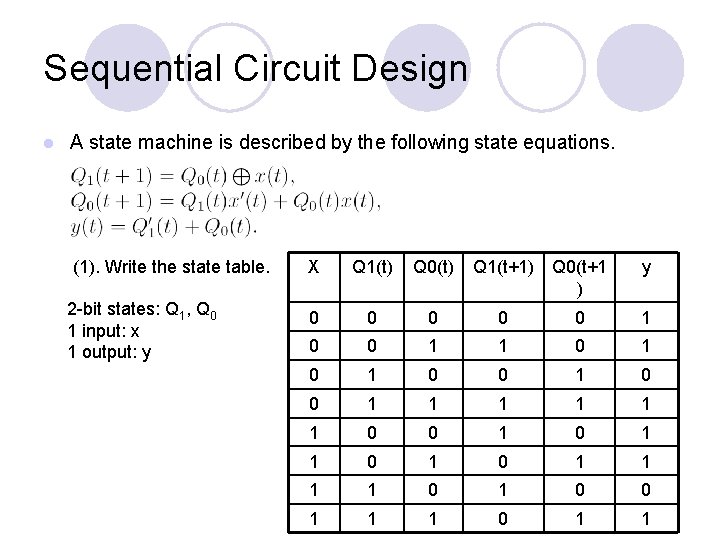
Sequential Circuit Design l A state machine is described by the following state equations. (1). Write the state table. 2 -bit states: Q 1, Q 0 1 input: x 1 output: y X Q 1(t) Q 0(t) Q 1(t+1) Q 0(t+1 ) y 0 0 0 1 1 0 1 0 0 1 1 1 0 0 1 0 1 1 1 1 0 0 1 1 1 0 1 1

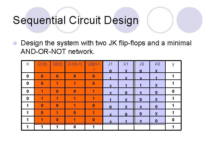
Sequential Circuit Design l Design the system with two JK flip-flops and a minimal AND-OR-NOT network. X Q 1(t) Q 0(t) Q 1(t+1) Q 0(t+1 ) J 1 K 1 J 0 K 0 0 X 1 X x 1 1 X y 0 0 0 1 0 0 1 x 0 0 0 1 1 1 X 0 X 1 1 0 0 X x 0 1 1 0 1 x 0 0 X 1 1 1 0 x 1 x 0 0 1 1 1

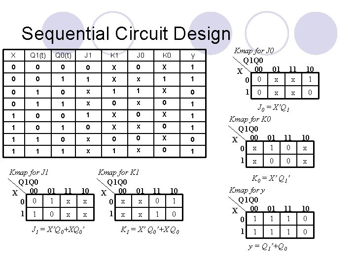
Sequential Circuit Design X Q 1(t) Q 0(t) J 1 K 1 J 0 K 0 y 0 0 X 0 X 1 0 0 1 1 X x 1 1 0 x 1 1 X 0 0 1 1 x 0 1 1 0 0 1 X 0 X 1 1 0 X x 0 1 1 1 0 x 0 0 X 0 1 1 1 x 0 1 Kmap for J 0 Q 1 Q 0 00 01 X x 0 0 1 0 x 1 1 0 11 x 10 x x x J 1 = X’Q 0+XQ 0’ Kmap for K 1 Q 1 Q 0 00 01 X x 0 x 1 x x 11 0 10 1 1 0 K 1 = X’ Q 0’+X Q 0 10 1 x 0 J 0 = X’Q 1 Kmap for K 0 Q 1 Q 0 00 01 11 X 1 0 0 x 1 Kmap for J 1 Q 1 Q 0 00 01 X 1 0 0 11 x 0 x K 0 = X’ Q 1’ Kmap for y Q 1 Q 0 00 01 11 X 1 1 0 1 10 0 1 x 1 0 10 x 1 y = Q 1’+Q 0 1 0

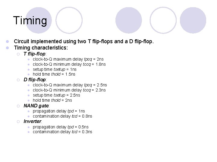
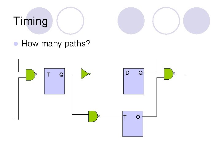
Timing l l Circuit implemented using two T flip-flops and a D flip-flop. Timing characteristics: ¡ T flip-flop: l l ¡ D flip-flop: l l ¡ clock-to-Q maximum delay tpcq = 2. 5 ns clock-to-Q minimum delay tccq = 2. 3 ns setup time tsetup = 2. 5 ns hold time thold = 2 ns NAND gate: l l ¡ clock-to-Q maximum delay tpcq = 2 ns clock-to-Q minimum delay tccq = 1. 8 ns setup time tsetup = 1 ns hold time thold = 1. 5 ns propagation delay tpd = 1 ns contamination delay tcd = 0. 8 ns Inverter: l l propagation delay tpd = 0. 5 ns contamination delay tcd = 0. 3 ns

Timing l How many paths? T Q D T Q Q

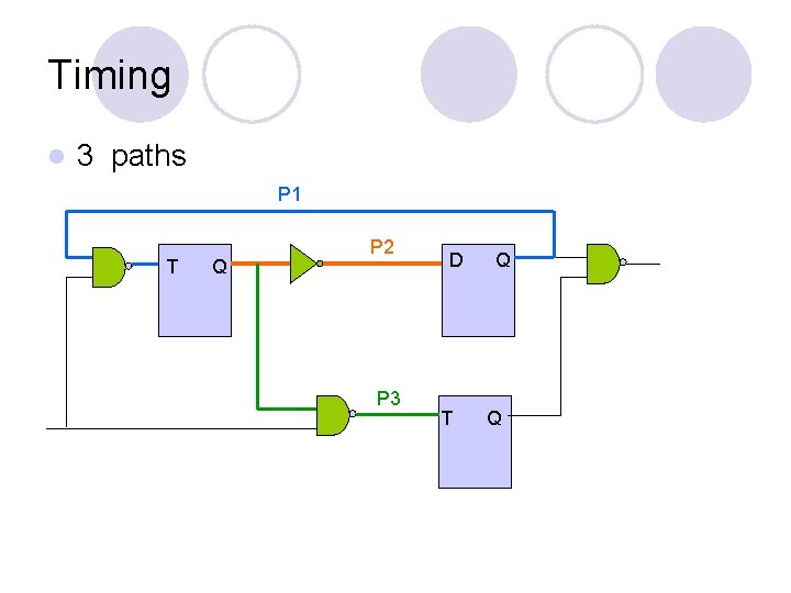
Timing l 3 paths P 1 T Q P 2 P 3 D T Q Q

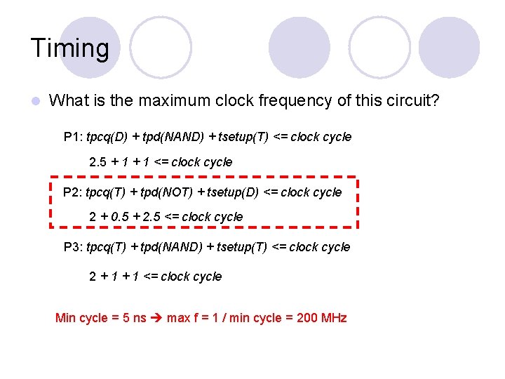
Timing l What is the maximum clock frequency of this circuit? P 1: tpcq(D) + tpd(NAND) + tsetup(T) <= clock cycle 2. 5 + 1 <= clock cycle P 2: tpcq(T) + tpd(NOT) + tsetup(D) <= clock cycle 2 + 0. 5 + 2. 5 <= clock cycle P 3: tpcq(T) + tpd(NAND) + tsetup(T) <= clock cycle 2 + 1 <= clock cycle Min cycle = 5 ns max f = 1 / min cycle = 200 MHz

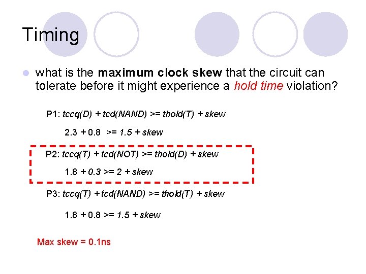
Timing l what is the maximum clock skew that the circuit can tolerate before it might experience a hold time violation? P 1: tccq(D) + tcd(NAND) >= thold(T) + skew 2. 3 + 0. 8 >= 1. 5 + skew P 2: tccq(T) + tcd(NOT) >= thold(D) + skew 1. 8 + 0. 3 >= 2 + skew P 3: tccq(T) + tcd(NAND) >= thold(T) + skew 1. 8 + 0. 8 >= 1. 5 + skew Max skew = 0. 1 ns

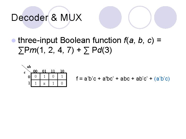
Decoder & MUX l three-input Boolean function f(a, b, c) = ∑Pm(1, 2, 4, 7) + ∑ Pd(3) ab c 00 0 0 1 1 01 1 11 0 10 1 x 1 0 f = a’b’c + a'bc’ + abc + ab’c’ + (a’b’c)

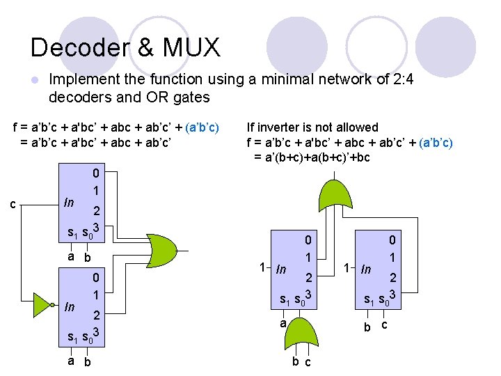
Decoder & MUX l Implement the function using a minimal network of 2: 4 decoders and OR gates f = a’b’c + a'bc’ + abc + ab’c’ + (a’b’c) = a’b’c + a'bc’ + abc + ab’c’ c In If inverter is not allowed f = a’b’c + a'bc’ + abc + ab’c’ + (a’b’c) = a’(b+c)+a(b+c)’+bc 0 1 2 s 1 s 03 a b In 0 1 2 s 1 s 03 a b 1 In 0 1 2 s 1 s 03 a 1 In 2 s 1 s 03 b c 0 1

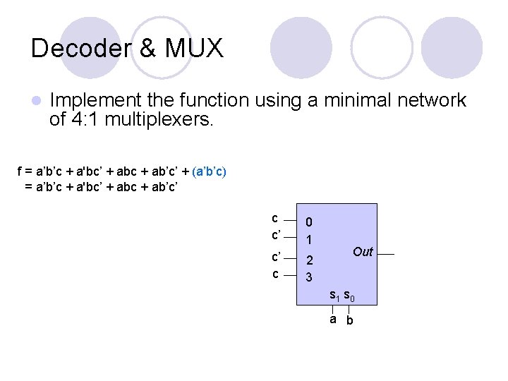
Decoder & MUX l Implement the function using a minimal network of 4: 1 multiplexers. f = a’b’c + a'bc’ + abc + ab’c’ + (a’b’c) = a’b’c + a'bc’ + abc + ab’c’ c c’ 0 1 c’ c 2 3 Out s 1 s 0 a b

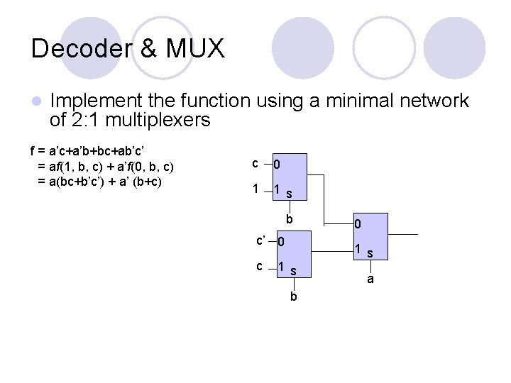
Decoder & MUX l Implement the function using a minimal network of 2: 1 multiplexers f = a’c+a’b+bc+ab’c’ = af(1, b, c) + a’f(0, b, c) = a(bc+b’c’) + a’ (b+c) c 0 1 1 s b c’ 0 c 1 s b 0 1 s a