CS 252 Graduate Computer Architecture Lecture 22 Memory

- Slides: 44
CS 252 Graduate Computer Architecture Lecture 22 Memory Technology Error Correction Codes April 16 th, 2012 John Kubiatowicz Electrical Engineering and Computer Sciences University of California, Berkeley http: //www. eecs. berkeley. edu/~kubitron/cs 252
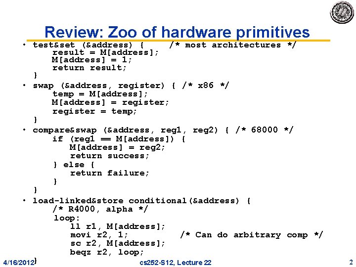
Review: Zoo of hardware primitives • test&set (&address) { /* most architectures */ result = M[address]; M[address] = 1; return result; } • swap (&address, register) { /* x 86 */ temp = M[address]; M[address] = register; register = temp; } • compare&swap (&address, reg 1, reg 2) { /* 68000 */ if (reg 1 == M[address]) { M[address] = reg 2; return success; } else { return failure; } } • load-linked&store conditional(&address) { /* R 4000, alpha */ loop: ll r 1, M[address]; movi r 2, 1; /* Can do arbitrary comp */ sc r 2, M[address]; beqz r 2, loop; 4/16/2012} cs 252 S 12, Lecture 22 2
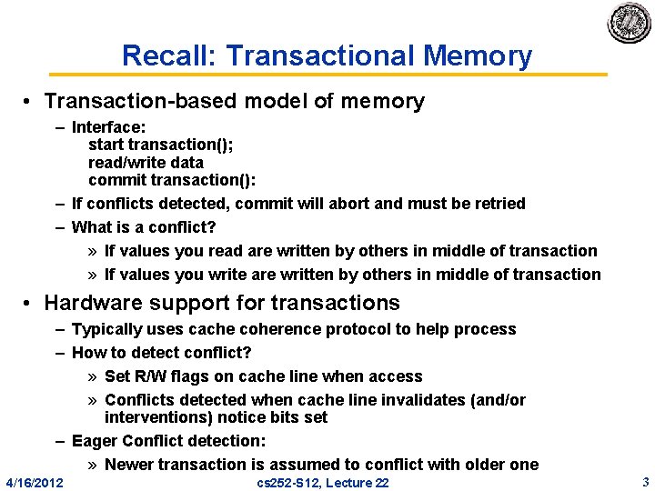
Recall: Transactional Memory • Transaction based model of memory – Interface: start transaction(); read/write data commit transaction(): – If conflicts detected, commit will abort and must be retried – What is a conflict? » If values you read are written by others in middle of transaction » If values you write are written by others in middle of transaction • Hardware support for transactions – Typically uses cache coherence protocol to help process – How to detect conflict? » Set R/W flags on cache line when access » Conflicts detected when cache line invalidates (and/or interventions) notice bits set – Eager Conflict detection: » Newer transaction is assumed to conflict with older one 4/16/2012 cs 252 S 12, Lecture 22 3
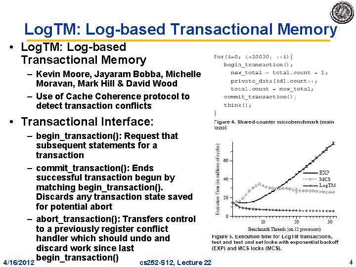
Log. TM: Log based Transactional Memory • Log. TM: Log based Transactional Memory – Kevin Moore, Jayaram Bobba, Michelle Moravan, Mark Hill & David Wood – Use of Cache Coherence protocol to detect transaction conflicts • Transactional Interface: – begin_transaction(): Request that subsequent statements for a transaction – commit_transaction(): Ends successful transaction begun by matching begin_transaction(). Discards any transaction state saved for potential abort – abort_transaction(): Transfers control to a previously register conflict handler which should undo and discard work since last begin_transaction() 4/16/2012 cs 252 S 12, Lecture 22 4
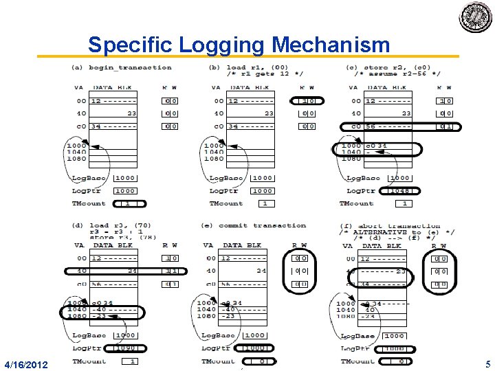
Specific Logging Mechanism 4/16/2012 cs 252 S 12, Lecture 22 5
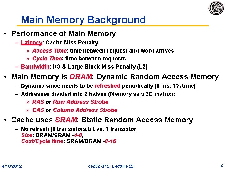
Main Memory Background • Performance of Main Memory: – Latency: Cache Miss Penalty » Access Time: time between request and word arrives » Cycle Time: time between requests – Bandwidth: I/O & Large Block Miss Penalty (L 2) • Main Memory is DRAM: Dynamic Random Access Memory – Dynamic since needs to be refreshed periodically (8 ms, 1% time) – Addresses divided into 2 halves (Memory as a 2 D matrix): » RAS or Row Address Strobe » CAS or Column Address Strobe • Cache uses SRAM: Static Random Access Memory – No refresh (6 transistors/bit vs. 1 transistor Size: DRAM/SRAM 4 -8, Cost/Cycle time: SRAM/DRAM 8 -16 4/16/2012 cs 252 S 12, Lecture 22 6
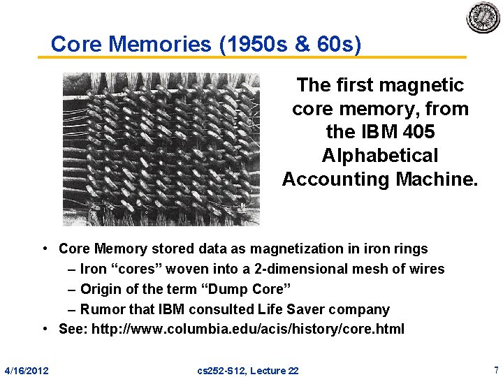
Core Memories (1950 s & 60 s) The first magnetic core memory, from the IBM 405 Alphabetical Accounting Machine. • Core Memory stored data as magnetization in iron rings – Iron “cores” woven into a 2 dimensional mesh of wires – Origin of the term “Dump Core” – Rumor that IBM consulted Life Saver company • See: http: //www. columbia. edu/acis/history/core. html 4/16/2012 cs 252 S 12, Lecture 22 7
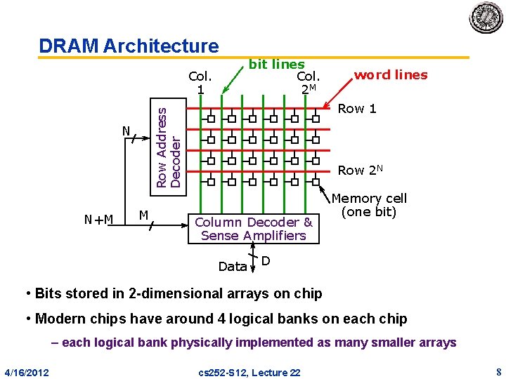
DRAM Architecture Col. 1 M word lines Row 1 Row Address Decoder N N+M bit lines Col. 2 M Row 2 N Column Decoder & Sense Amplifiers Data Memory cell (one bit) D • Bits stored in 2 dimensional arrays on chip • Modern chips have around 4 logical banks on each chip – each logical bank physically implemented as many smaller arrays 4/16/2012 cs 252 S 12, Lecture 22 8
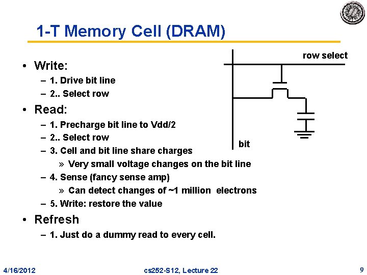
1 T Memory Cell (DRAM) row select • Write: – 1. Drive bit line – 2. . Select row • Read: – 1. Precharge bit line to Vdd/2 – 2. . Select row bit – 3. Cell and bit line share charges » Very small voltage changes on the bit line – 4. Sense (fancy sense amp) » Can detect changes of ~1 million electrons – 5. Write: restore the value • Refresh – 1. Just do a dummy read to every cell. 4/16/2012 cs 252 S 12, Lecture 22 9
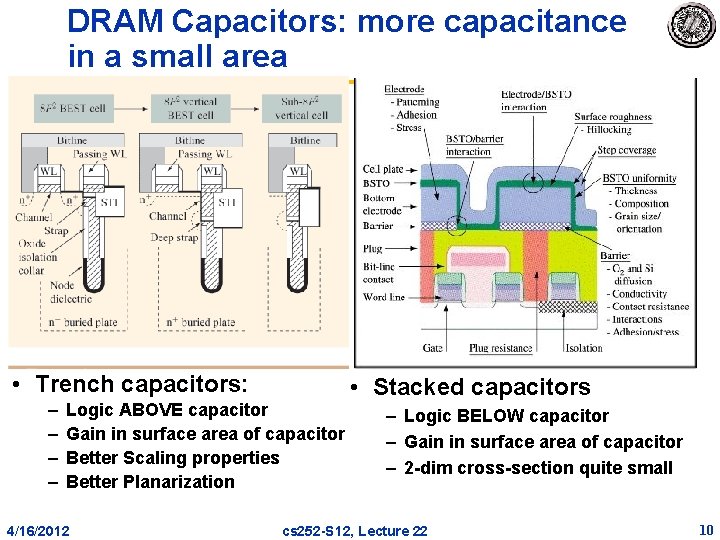
DRAM Capacitors: more capacitance in a small area • Trench capacitors: – – Logic ABOVE capacitor Gain in surface area of capacitor Better Scaling properties Better Planarization 4/16/2012 • Stacked capacitors – Logic BELOW capacitor – Gain in surface area of capacitor – 2 dim cross section quite small cs 252 S 12, Lecture 22 10
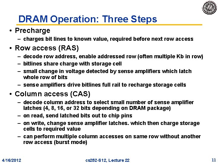
DRAM Operation: Three Steps • Precharge – charges bit lines to known value, required before next row access • Row access (RAS) – decode row address, enable addressed row (often multiple Kb in row) – bitlines share charge with storage cell – small change in voltage detected by sense amplifiers which latch whole row of bits – sense amplifiers drive bitlines full rail to recharge storage cells • Column access (CAS) – decode column address to select small number of sense amplifier latches (4, 8, 16, or 32 bits depending on DRAM package) – on read, send latched bits out to chip pins – on write, change sense amplifier latches. which then charge storage cells to required value – can perform multiple column accesses on same row without another row access (burst mode) 4/16/2012 cs 252 S 12, Lecture 22 11
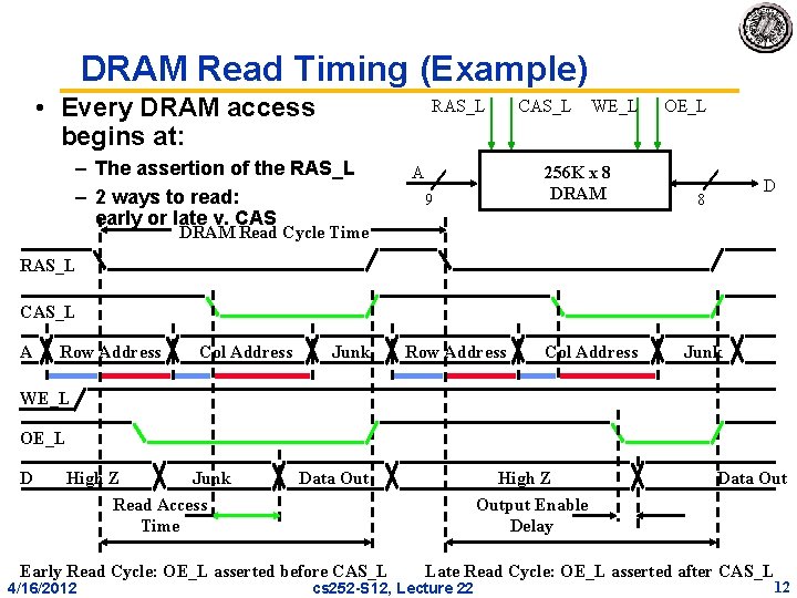
DRAM Read Timing (Example) • Every DRAM access begins at: RAS_L – The assertion of the RAS_L – 2 ways to read: early or late v. CAS_L WE_L 256 K x 8 DRAM A 9 OE_L D 8 DRAM Read Cycle Time RAS_L CAS_L A Row Address Col Address Junk WE_L OE_L D High Z Junk Read Access Time Data Out Early Read Cycle: OE_L asserted before CAS_L 4/16/2012 High Z Output Enable Delay Data Out Late Read Cycle: OE_L asserted after CAS_L cs 252 S 12, Lecture 22 12
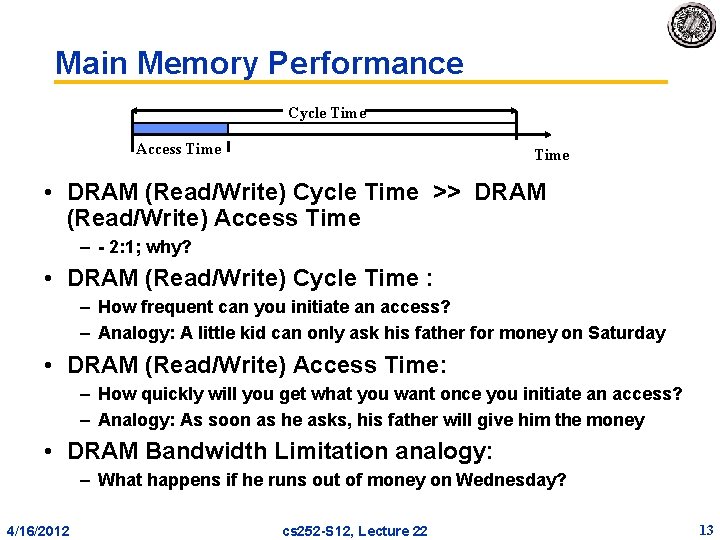
Main Memory Performance Cycle Time Access Time • DRAM (Read/Write) Cycle Time >> DRAM (Read/Write) Access Time – 2: 1; why? • DRAM (Read/Write) Cycle Time : – How frequent can you initiate an access? – Analogy: A little kid can only ask his father for money on Saturday • DRAM (Read/Write) Access Time: – How quickly will you get what you want once you initiate an access? – Analogy: As soon as he asks, his father will give him the money • DRAM Bandwidth Limitation analogy: – What happens if he runs out of money on Wednesday? 4/16/2012 cs 252 S 12, Lecture 22 13
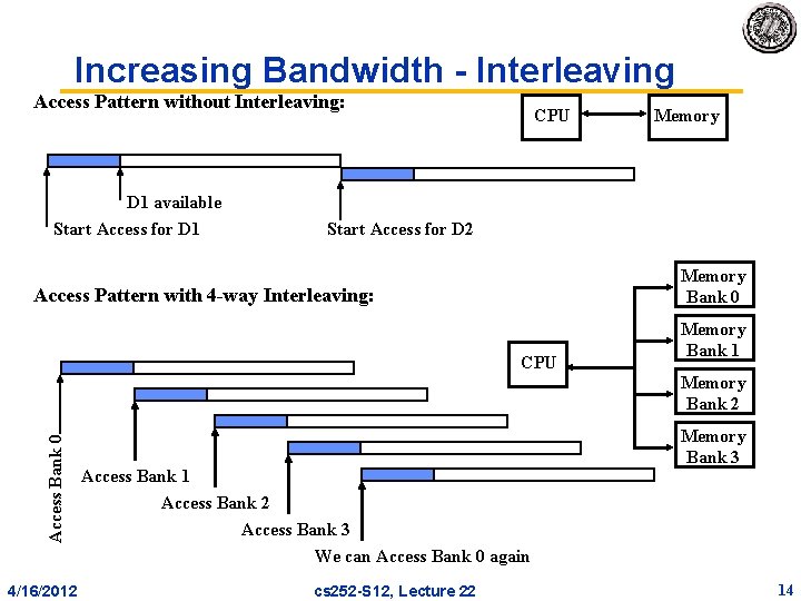
Increasing Bandwidth Interleaving Access Pattern without Interleaving: D 1 available Start Access for D 1 CPU Memory Start Access for D 2 Memory Bank 0 Access Pattern with 4 -way Interleaving: CPU Memory Bank 1 Access Bank 0 Memory Bank 2 4/16/2012 Access Bank 1 Access Bank 2 Access Bank 3 We can Access Bank 0 again cs 252 S 12, Lecture 22 Memory Bank 3 14
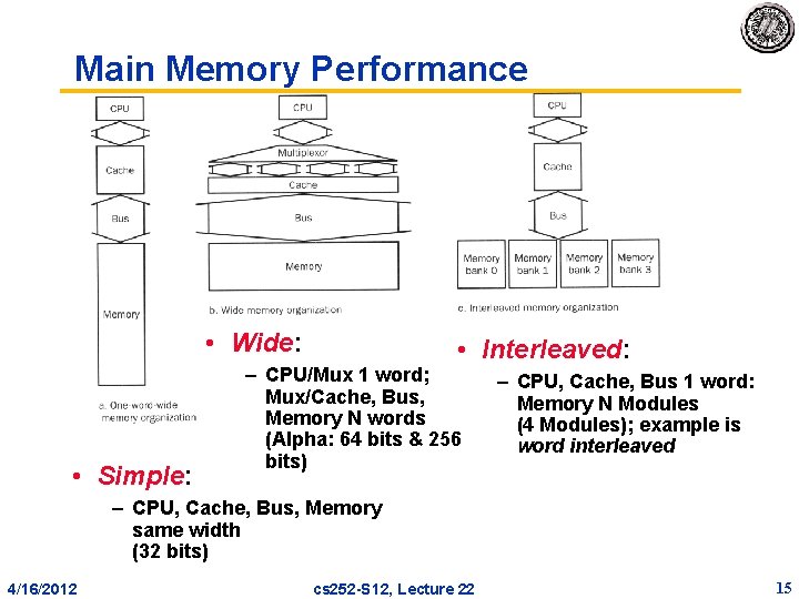
Main Memory Performance • Wide: • Simple: • Interleaved: – CPU/Mux 1 word; Mux/Cache, Bus, Memory N words (Alpha: 64 bits & 256 bits) – CPU, Cache, Bus 1 word: Memory N Modules (4 Modules); example is word interleaved – CPU, Cache, Bus, Memory same width (32 bits) 4/16/2012 cs 252 S 12, Lecture 22 15
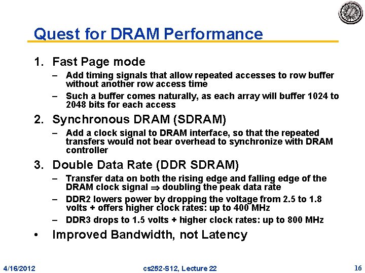
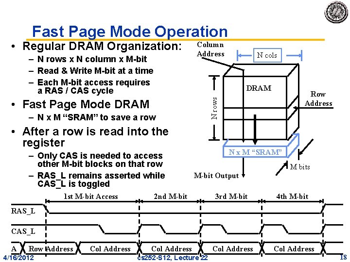
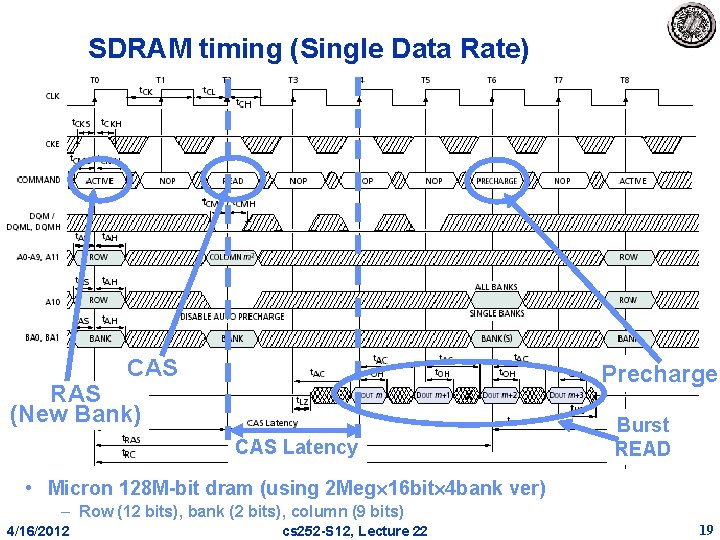
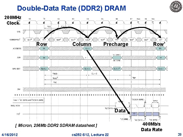
Quest for DRAM Performance 1. Fast Page mode – Add timing signals that allow repeated accesses to row buffer without another row access time – Such a buffer comes naturally, as each array will buffer 1024 to 2048 bits for each access 2. Synchronous DRAM (SDRAM) – Add a clock signal to DRAM interface, so that the repeated transfers would not bear overhead to synchronize with DRAM controller 3. Double Data Rate (DDR SDRAM) – Transfer data on both the rising edge and falling edge of the DRAM clock signal doubling the peak data rate – DDR 2 lowers power by dropping the voltage from 2. 5 to 1. 8 volts + offers higher clock rates: up to 400 MHz – DDR 3 drops to 1. 5 volts + higher clock rates: up to 800 MHz • 4/16/2012 Improved Bandwidth, not Latency cs 252 S 12, Lecture 22 16
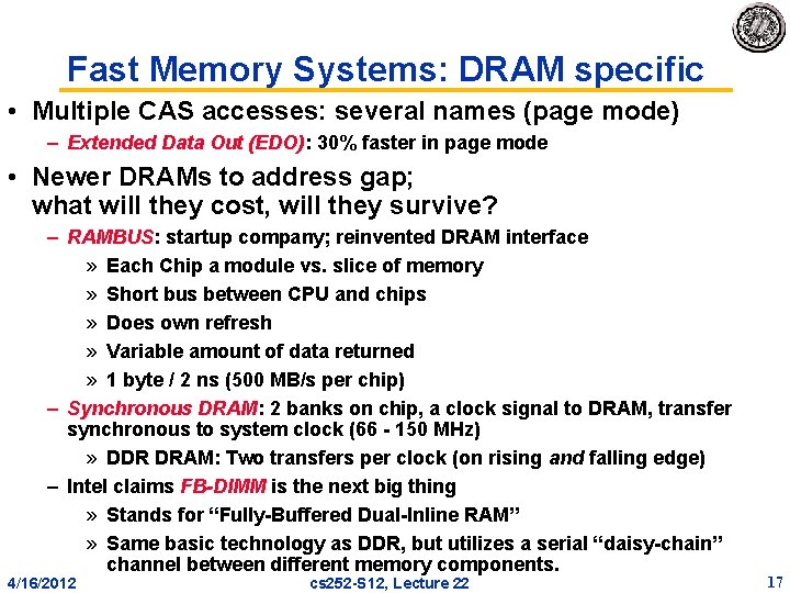
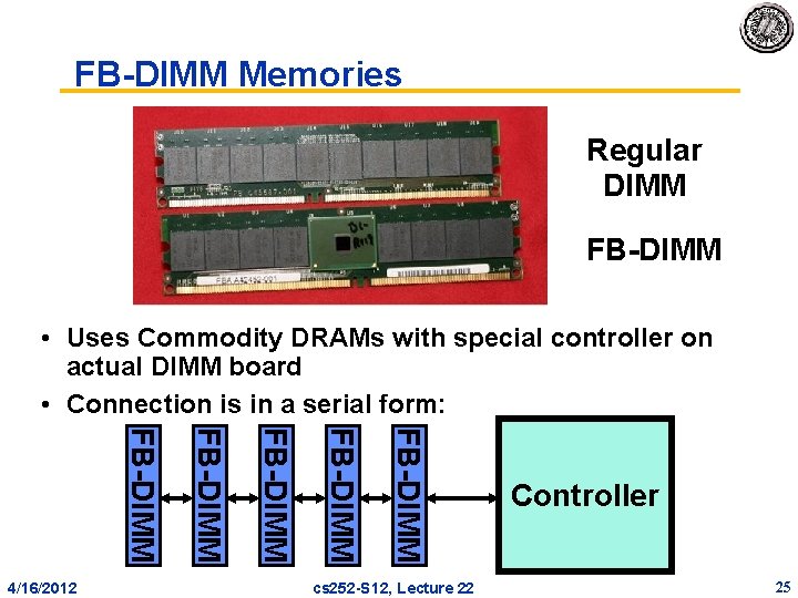
Fast Memory Systems: DRAM specific • Multiple CAS accesses: several names (page mode) – Extended Data Out (EDO): 30% faster in page mode • Newer DRAMs to address gap; what will they cost, will they survive? – RAMBUS: startup company; reinvented DRAM interface » Each Chip a module vs. slice of memory » Short bus between CPU and chips » Does own refresh » Variable amount of data returned » 1 byte / 2 ns (500 MB/s per chip) – Synchronous DRAM: 2 banks on chip, a clock signal to DRAM, transfer synchronous to system clock (66 150 MHz) » DDR DRAM: Two transfers per clock (on rising and falling edge) – Intel claims FB-DIMM is the next big thing » Stands for “Fully Buffered Dual Inline RAM” » Same basic technology as DDR, but utilizes a serial “daisy chain” channel between different memory components. 4/16/2012 cs 252 S 12, Lecture 22 17
Fast Page Mode Operation • Regular DRAM Organization: – N rows x N column x M bit – Read & Write M bit at a time – Each M bit access requires a RAS / CAS cycle Column Address DRAM – N x M “SRAM” to save a row • After a row is read into the register – Only CAS is needed to access other M bit blocks on that row – RAS_L remains asserted while CAS_L is toggled Row Address N rows • Fast Page Mode DRAM 1 st M-bit Access N cols N x M “SRAM” M bits M-bit Output 2 nd M-bit 3 rd M-bit 4 th M-bit Col Address RAS_L CAS_L A Row Address 4/16/2012 Col Address cs 252 S 12, Lecture 22 18
SDRAM timing (Single Data Rate) CAS RAS (New Bank) x CAS Latency Precharge Burst READ • Micron 128 M bit dram (using 2 Meg 16 bit 4 bank ver) – Row (12 bits), bank (2 bits), column (9 bits) 4/16/2012 cs 252 S 12, Lecture 22 19
Double Data Rate (DDR 2) DRAM 200 MHz Clock Row Column Precharge Row’ Data [ Micron, 256 Mb DDR 2 SDRAM datasheet ] 4/16/2012 cs 252 S 12, Lecture 22 400 Mb/s Data Rate 20
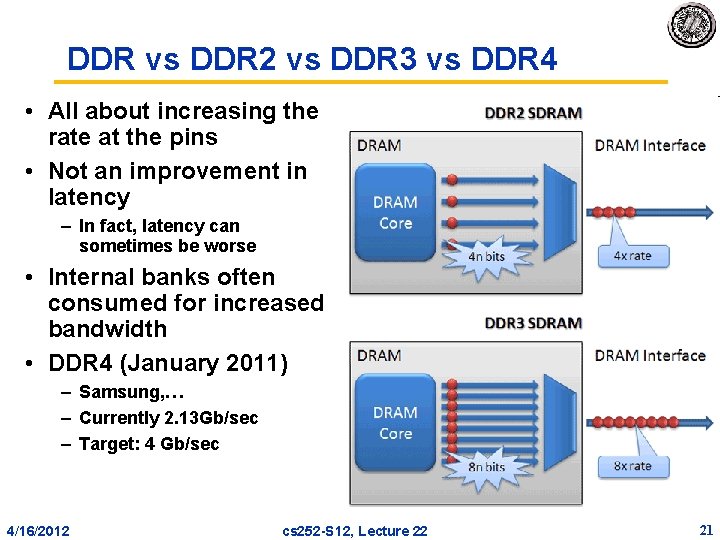
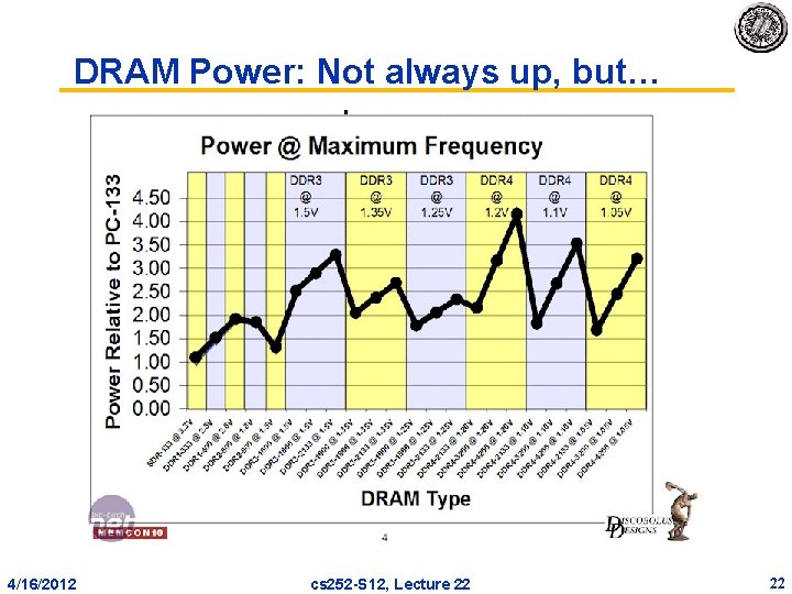
DDR vs DDR 2 vs DDR 3 vs DDR 4 • All about increasing the rate at the pins • Not an improvement in latency – In fact, latency can sometimes be worse • Internal banks often consumed for increased bandwidth • DDR 4 (January 2011) – Samsung, … – Currently 2. 13 Gb/sec – Target: 4 Gb/sec 4/16/2012 cs 252 S 12, Lecture 22 21
DRAM Power: Not always up, but… 4/16/2012 cs 252 S 12, Lecture 22 22
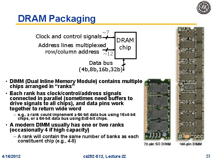
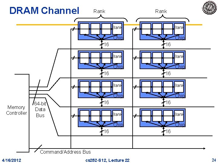
DRAM Packaging Clock and control signals ~7 Address lines multiplexed row/column address ~12 DRAM chip Data bus (4 b, 8 b, 16 b, 32 b) • DIMM (Dual Inline Memory Module) contains multiple chips arranged in “ranks” • Each rank has clock/control/address signals connected in parallel (sometimes need buffers to drive signals to all chips), and data pins work together to return wide word – e. g. , a rank could implement a 64 bit data bus using 16 x 4 bit chips, or a 64 bit data bus using 8 x 8 bit chips. • A modern DIMM usually has one or two ranks (occasionally 4 if high capacity) – A rank will contain the same number of banks as each constituent chip (e. g. , 4 8) 4/16/2012 cs 252 S 12, Lecture 22 23
DRAM Channel Rank Bank Chip 16 16 Bank Chip 16 Memory Controller 16 Bank Chip 16 64 -bit Data Bus 16 Bank Chip 16 16 Command/Address Bus 4/16/2012 cs 252 S 12, Lecture 22 24
FB DIMM Memories Regular DIMM FB DIMM • Uses Commodity DRAMs with special controller on actual DIMM board • Connection is in a serial form: FB DIMM FB DIMM 4/16/2012 cs 252 S 12, Lecture 22 Controller 25
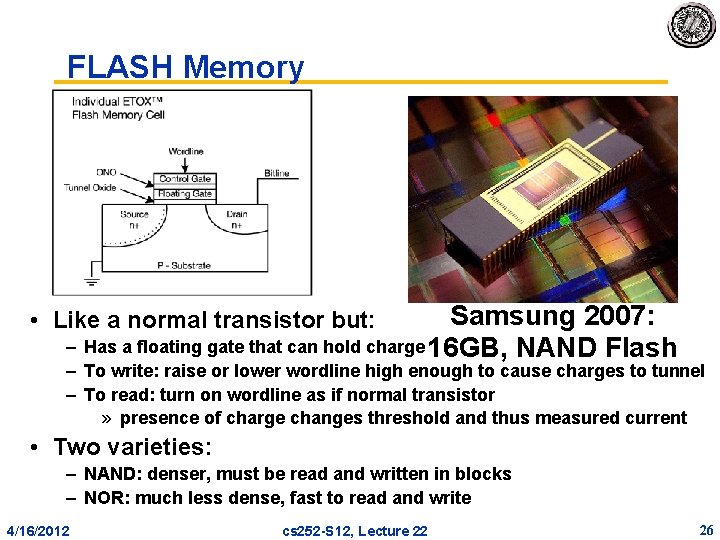
FLASH Memory Samsung 2007: – Has a floating gate that can hold charge 16 GB, NAND Flash • Like a normal transistor but: – To write: raise or lower wordline high enough to cause charges to tunnel – To read: turn on wordline as if normal transistor » presence of charge changes threshold and thus measured current • Two varieties: – NAND: denser, must be read and written in blocks – NOR: much less dense, fast to read and write 4/16/2012 cs 252 S 12, Lecture 22 26
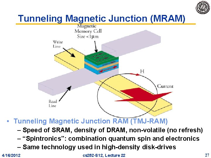
Tunneling Magnetic Junction (MRAM) • Tunneling Magnetic Junction RAM (TMJ RAM) – Speed of SRAM, density of DRAM, non volatile (no refresh) – “Spintronics”: combination quantum spin and electronics – Same technology used in high density disk drives 4/16/2012 cs 252 S 12, Lecture 22 27
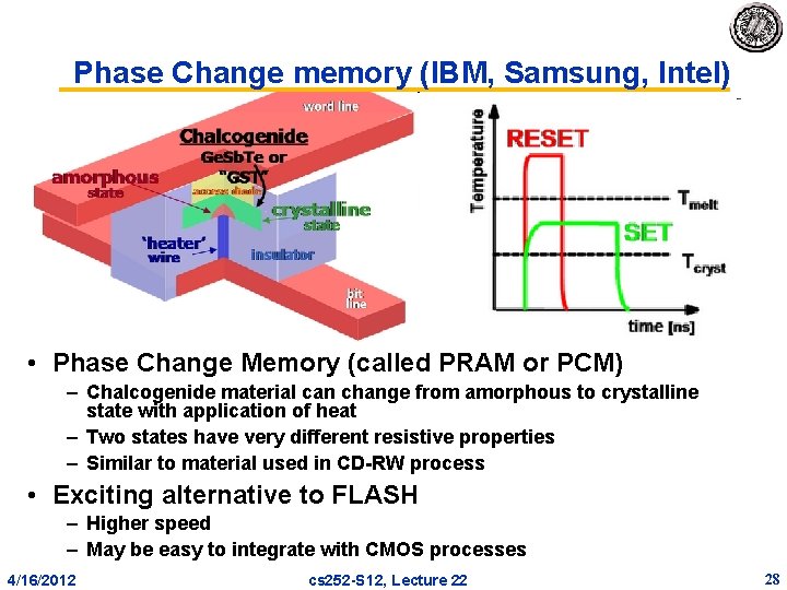
Phase Change memory (IBM, Samsung, Intel) • Phase Change Memory (called PRAM or PCM) – Chalcogenide material can change from amorphous to crystalline state with application of heat – Two states have very different resistive properties – Similar to material used in CD RW process • Exciting alternative to FLASH – Higher speed – May be easy to integrate with CMOS processes 4/16/2012 cs 252 S 12, Lecture 22 28
Error Correction Codes (ECC) • Memory systems generate errors (accidentally flipped bits) – DRAMs store very little charge per bit – “Soft” errors occur occasionally when cells are struck by alpha particles or other environmental upsets. – Less frequently, “hard” errors can occur when chips permanently fail. – Problem gets worse as memories get denser and larger • Where is “perfect” memory required? – servers, spacecraft/military computers, ebay, … • Memories are protected against failures with ECCs • Extra bits are added to each data word – used to detect and/or correct faults in the memory system – in general, each possible data word value is mapped to a unique “code word”. A fault changes a valid code word to an invalid one which can be detected. 4/16/2012 cs 252 S 12, Lecture 22 29
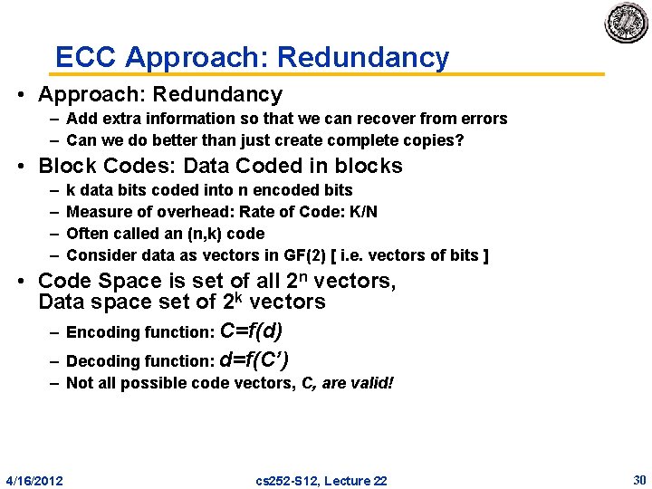
ECC Approach: Redundancy • Approach: Redundancy – Add extra information so that we can recover from errors – Can we do better than just create complete copies? • Block Codes: Data Coded in blocks – – k data bits coded into n encoded bits Measure of overhead: Rate of Code: K/N Often called an (n, k) code Consider data as vectors in GF(2) [ i. e. vectors of bits ] • Code Space is set of all 2 n vectors, Data space set of 2 k vectors – Encoding function: C=f(d) – Decoding function: d=f(C’) – Not all possible code vectors, C, are valid! 4/16/2012 cs 252 S 12, Lecture 22 30
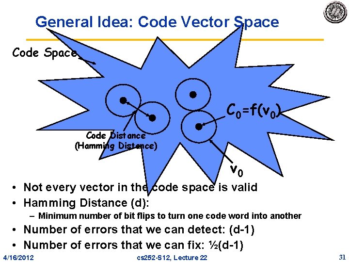
General Idea: Code Vector Space Code Space C 0=f(v 0) Code Distance (Hamming Distance) v 0 • Not every vector in the code space is valid • Hamming Distance (d): – Minimum number of bit flips to turn one code word into another • Number of errors that we can detect: (d 1) • Number of errors that we can fix: ½(d 1) 4/16/2012 cs 252 S 12, Lecture 22 31
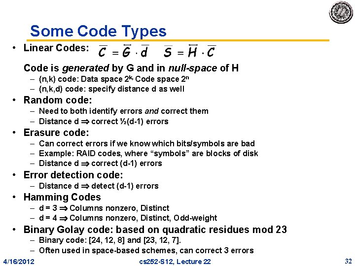
Some Code Types • Linear Codes: Code is generated by G and in null-space of H – (n, k) code: Data space 2 k, Code space 2 n – (n, k, d) code: specify distance d as well • Random code: – Need to both identify errors and correct them – Distance d correct ½(d 1) errors • Erasure code: – Can correct errors if we know which bits/symbols are bad – Example: RAID codes, where “symbols” are blocks of disk – Distance d correct (d 1) errors • Error detection code: – Distance d detect (d 1) errors • Hamming Codes – d = 3 Columns nonzero, Distinct – d = 4 Columns nonzero, Distinct, Odd weight • Binary Golay code: based on quadratic residues mod 23 – Binary code: [24, 12, 8] and [23, 12, 7]. – Often used in space based schemes, can correct 3 errors 4/16/2012 cs 252 S 12, Lecture 22 32
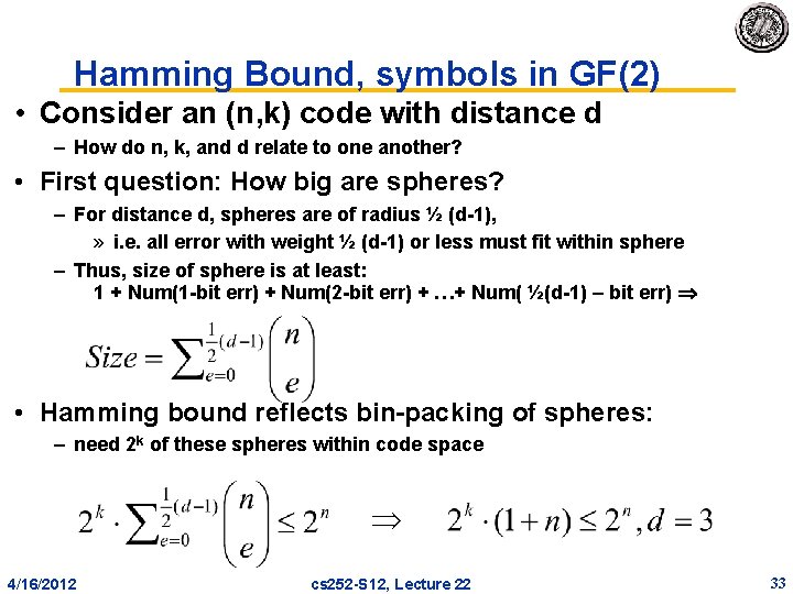
Hamming Bound, symbols in GF(2) • Consider an (n, k) code with distance d – How do n, k, and d relate to one another? • First question: How big are spheres? – For distance d, spheres are of radius ½ (d 1), » i. e. all error with weight ½ (d 1) or less must fit within sphere – Thus, size of sphere is at least: 1 + Num(1 bit err) + Num(2 bit err) + …+ Num( ½(d 1) – bit err) • Hamming bound reflects bin packing of spheres: – need 2 k of these spheres within code space 4/16/2012 cs 252 S 12, Lecture 22 33
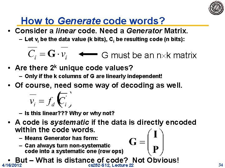
How to Generate code words? • Consider a linear code. Need a Generator Matrix. – Let vi be the data value (k bits), Ci be resulting code (n bits): G must be an n k matrix • Are there 2 k unique code values? – Only if the k columns of G are linearly independent! • Of course, need some way of decoding as well. – Is this linear? ? ? Why or why not? • A code is systematic if the data is directly encoded within the code words. – Means Generator has form: – Can always turn non systematic code into a systematic one (row ops) • But – What is distance of code? Not Obvious! 4/16/2012 cs 252 S 12, Lecture 22 34
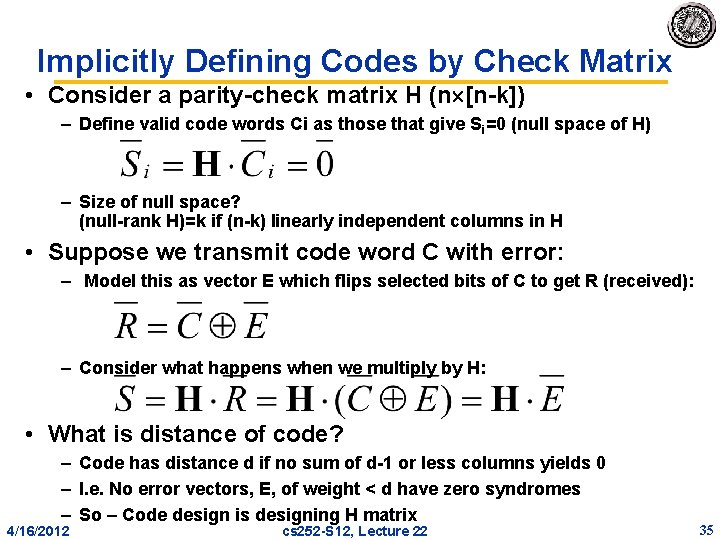
Implicitly Defining Codes by Check Matrix • Consider a parity check matrix H (n [n k]) – Define valid code words Ci as those that give Si=0 (null space of H) – Size of null space? (null rank H)=k if (n k) linearly independent columns in H • Suppose we transmit code word C with error: – Model this as vector E which flips selected bits of C to get R (received): – Consider what happens when we multiply by H: • What is distance of code? – Code has distance d if no sum of d 1 or less columns yields 0 – I. e. No error vectors, E, of weight < d have zero syndromes – So – Code design is designing H matrix 4/16/2012 cs 252 S 12, Lecture 22 35
How to relate G and H (Binary Codes) • Defining H makes it easy to understand distance of code, but hard to generate code (H defines code implicitly!) • However, let H be of following form: P is (n-k) k, I is (n-k) Result: H is (n-k) n • Then, G can be of following form (maximal code size): P is (n-k) k, I is k k Result: G is n k • Notice: G generates values in null space of H and has k independent columns so generates 2 k unique values: 4/16/2012 cs 252 S 12, Lecture 22 36
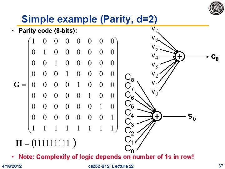
Simple example (Parity, d=2) • Parity code (8 bits): C 8 C 7 C 6 C 5 C 4 C 3 C 2 C 1 C 0 v 7 v 6 v 5 v 4 v 3 v 2 v 1 v 0 + c 8 + s 0 • Note: Complexity of logic depends on number of 1 s in row! 4/16/2012 cs 252 S 12, Lecture 22 37
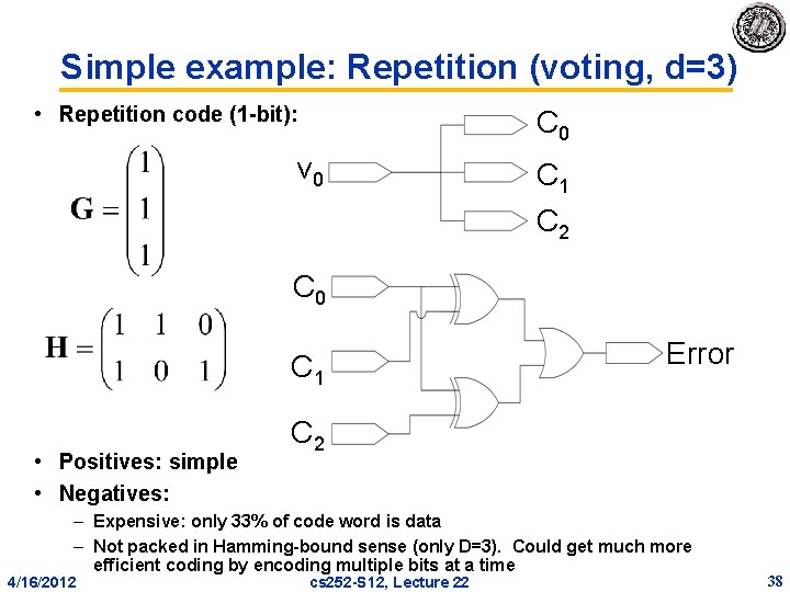
Simple example: Repetition (voting, d=3) • Repetition code (1 bit): C 0 v 0 C 1 C 2 C 0 C 1 • Positives: simple • Negatives: Error C 2 – Expensive: only 33% of code word is data – Not packed in Hamming bound sense (only D=3). Could get much more efficient coding by encoding multiple bits at a time 4/16/2012 cs 252 S 12, Lecture 22 38
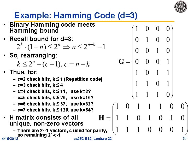
Example: Hamming Code (d=3) • Binary Hamming code meets Hamming bound • Recall bound for d=3: • So, rearranging: • Thus, for: – – – c=2 check bits, k ≤ 1 (Repetition code) c=3 check bits, k ≤ 4 c=4 check bits, k ≤ 11, use k=8? c=5 check bits, k ≤ 26, use k=16? c=6 check bits, k ≤ 57, use k=32? c=7 check bits, k ≤ 120, use k=64? • H matrix consists of all unique, non zero vectors – There are 2 c 1 vectors, c used for parity, so remaining 2 c c 1 4/16/2012 cs 252 S 12, Lecture 22 39
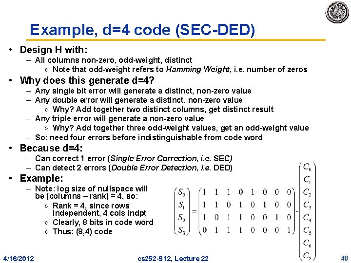
Example, d=4 code (SEC DED) • Design H with: – All columns non zero, odd weight, distinct » Note that odd weight refers to Hamming Weight, i. e. number of zeros • Why does this generate d=4? – Any single bit error will generate a distinct, non zero value – Any double error will generate a distinct, non zero value » Why? Add together two distinct columns, get distinct result – Any triple error will generate a non zero value » Why? Add together three odd weight values, get an odd weight value – So: need four errors before indistinguishable from code word • Because d=4: – Can correct 1 error (Single Error Correction, i. e. SEC) – Can detect 2 errors (Double Error Detection, i. e. DED) • Example: – Note: log size of nullspace will be (columns – rank) = 4, so: » Rank = 4, since rows independent, 4 cols indpt » Clearly, 8 bits in code word » Thus: (8, 4) code 4/16/2012 cs 252 S 12, Lecture 22 40
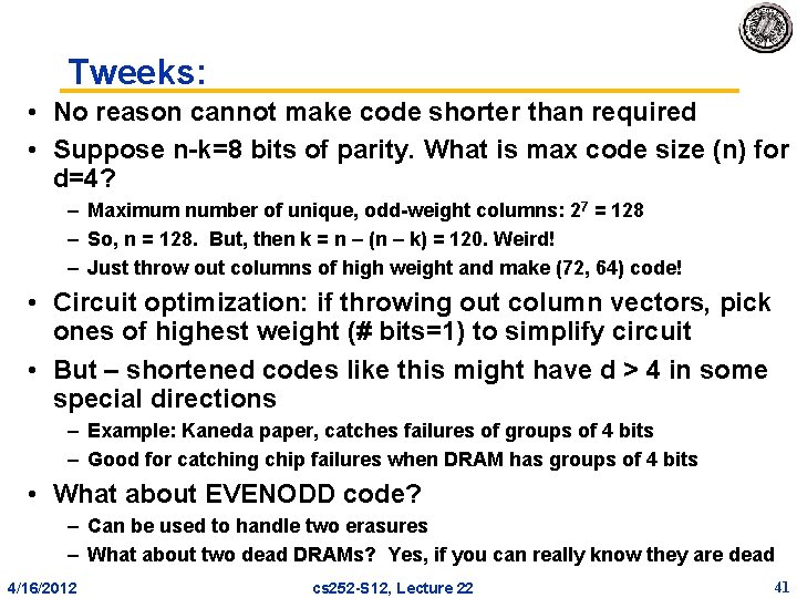
Tweeks: • No reason cannot make code shorter than required • Suppose n k=8 bits of parity. What is max code size (n) for d=4? – Maximum number of unique, odd weight columns: 27 = 128 – So, n = 128. But, then k = n – (n – k) = 120. Weird! – Just throw out columns of high weight and make (72, 64) code! • Circuit optimization: if throwing out column vectors, pick ones of highest weight (# bits=1) to simplify circuit • But – shortened codes like this might have d > 4 in some special directions – Example: Kaneda paper, catches failures of groups of 4 bits – Good for catching chip failures when DRAM has groups of 4 bits • What about EVENODD code? – Can be used to handle two erasures – What about two dead DRAMs? Yes, if you can really know they are dead 4/16/2012 cs 252 S 12, Lecture 22 41
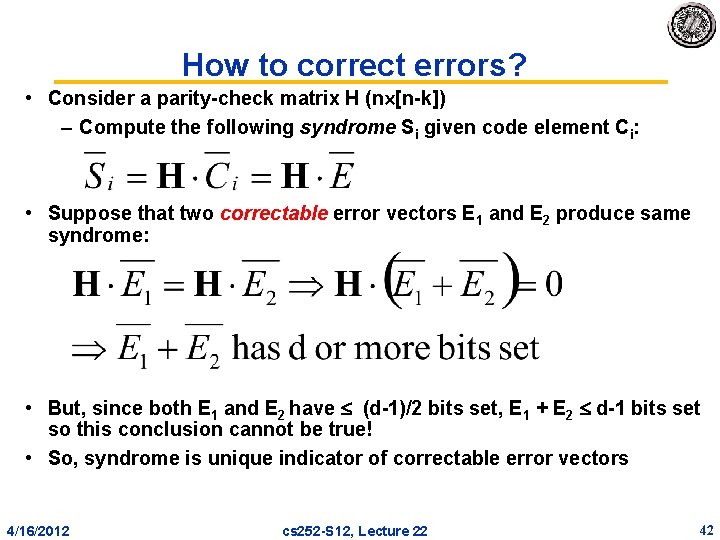
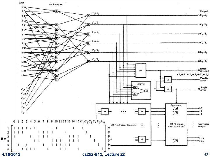
How to correct errors? • Consider a parity check matrix H (n [n k]) – Compute the following syndrome Si given code element Ci: • Suppose that two correctable error vectors E 1 and E 2 produce same syndrome: • But, since both E 1 and E 2 have (d 1)/2 bits set, E 1 + E 2 d 1 bits set so this conclusion cannot be true! • So, syndrome is unique indicator of correctable error vectors 4/16/2012 cs 252 S 12, Lecture 22 42
4/16/2012 cs 252 S 12, Lecture 22 43
Conclusion • Main memory is Dense, Slow – Cycle time > Access time! • Techniques to optimize memory – – Wider Memory Interleaved Memory: for sequential or independent accesses Avoiding bank conflicts: SW & HW DRAM specific optimizations: page mode & Specialty DRAM • ECC: add redundancy to correct for errors – (n, k, d) n code bits, k data bits, distance d – Linear codes: code vectors computed by linear transformation • Erasure code: after identifying “erasures”, can correct 4/16/2012 cs 252 S 12, Lecture 22 44