CS 184 a Computer Architecture Structure and Organization
![Area Perspective [2000 tech. ] 18 mm 0. 18 mm 60 G l 2 Area Perspective [2000 tech. ] 18 mm 0. 18 mm 60 G l 2](https://slidetodoc.com/presentation_image_h/c1d000d289ee05c5b6b9e41cc804ea33/image-11.jpg)
![MOS Transistor Scaling (1974 to present) S=0. 7 [0. 5 x per 2 nodes] MOS Transistor Scaling (1974 to present) S=0. 7 [0. 5 x per 2 nodes]](https://slidetodoc.com/presentation_image_h/c1d000d289ee05c5b6b9e41cc804ea33/image-25.jpg)
![Delays? • If delays in gates/switching? – Delay reduce with 1/k [l] Caltech CS Delays? • If delays in gates/switching? – Delay reduce with 1/k [l] Caltech CS](https://slidetodoc.com/presentation_image_h/c1d000d289ee05c5b6b9e41cc804ea33/image-30.jpg)
![Big Ideas [MSB Ideas] • Moderately predictable VLSI Scaling – unprecedented capacities/capability growth for Big Ideas [MSB Ideas] • Moderately predictable VLSI Scaling – unprecedented capacities/capability growth for](https://slidetodoc.com/presentation_image_h/c1d000d289ee05c5b6b9e41cc804ea33/image-47.jpg)
![Big Ideas [MSB-1 Ideas] • Uniform scaling reasonably accurate for past couple of decades Big Ideas [MSB-1 Ideas] • Uniform scaling reasonably accurate for past couple of decades](https://slidetodoc.com/presentation_image_h/c1d000d289ee05c5b6b9e41cc804ea33/image-48.jpg)
- Slides: 48

CS 184 a: Computer Architecture (Structure and Organization) Day 6: January 22, 2003 VLSI Scaling Caltech CS 184 Winter 2003 -- De. Hon 1

Today • • • VLSI Scaling Rules Effects Historical/predicted scaling Variations (cheating) Limits Caltech CS 184 Winter 2003 -- De. Hon 2

Why Care? • In this game, we must be able to predict the future • Rapid technology advance • Reason about changes and trends • re-evaluate prior solutions given technology at time X. Caltech CS 184 Winter 2003 -- De. Hon 3

Why Care • Cannot compare against what competitor does today – but what they can do at time you can ship • Careful not to fall off curve – lose out to someone who can stay on curve Caltech CS 184 Winter 2003 -- De. Hon 4

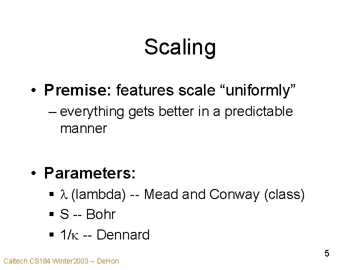
Scaling • Premise: features scale “uniformly” – everything gets better in a predictable manner • Parameters: § l (lambda) -- Mead and Conway (class) § S -- Bohr § 1/k -- Dennard Caltech CS 184 Winter 2003 -- De. Hon 5

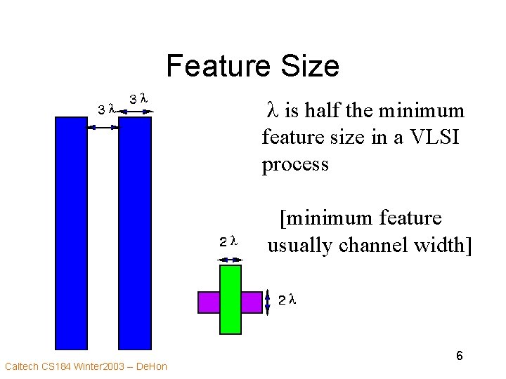
Feature Size l is half the minimum feature size in a VLSI process [minimum feature usually channel width] Caltech CS 184 Winter 2003 -- De. Hon 6

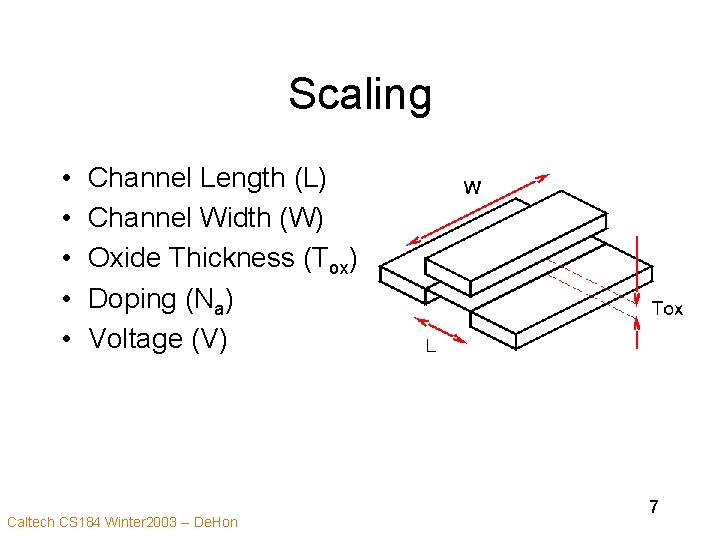
Scaling • • • Channel Length (L) Channel Width (W) Oxide Thickness (Tox) Doping (Na) Voltage (V) Caltech CS 184 Winter 2003 -- De. Hon 7

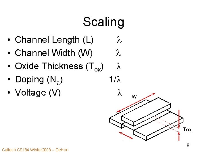
Scaling • • • Channel Length (L) l Channel Width (W) l Oxide Thickness (Tox) l Doping (Na) 1/l Voltage (V) l Caltech CS 184 Winter 2003 -- De. Hon 8

Effects? • • Area Capacitance Resistance Threshold (Vth) Current (Id) Gate Delay (tgd) Wire Delay (twire) Power Caltech CS 184 Winter 2003 -- De. Hon 9

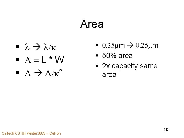
Area § l l/k § A = L * W § A A/k 2 Caltech CS 184 Winter 2003 -- De. Hon § 0. 35 mm 0. 25 mm § 50% area § 2 x capacity same area 10
![Area Perspective 2000 tech 18 mm 0 18 mm 60 G l 2 Area Perspective [2000 tech. ] 18 mm 0. 18 mm 60 G l 2](https://slidetodoc.com/presentation_image_h/c1d000d289ee05c5b6b9e41cc804ea33/image-11.jpg)
Area Perspective [2000 tech. ] 18 mm 0. 18 mm 60 G l 2 Caltech CS 184 Winter 2003 -- De. Hon 11

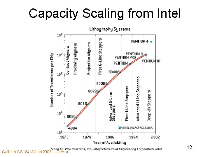
Capacity Scaling from Intel Caltech CS 184 Winter 2003 -- De. Hon 12

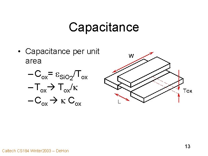
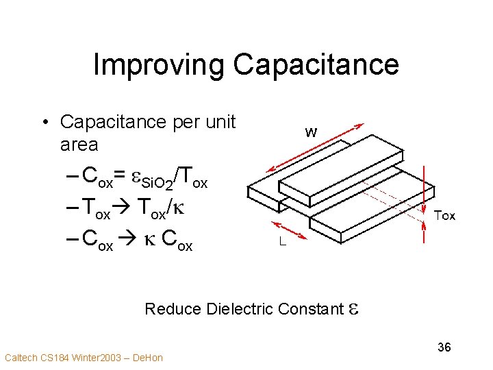
Capacitance • Capacitance per unit area – Cox= e. Si. O 2/Tox – Tox/k – Cox k Cox Caltech CS 184 Winter 2003 -- De. Hon 13

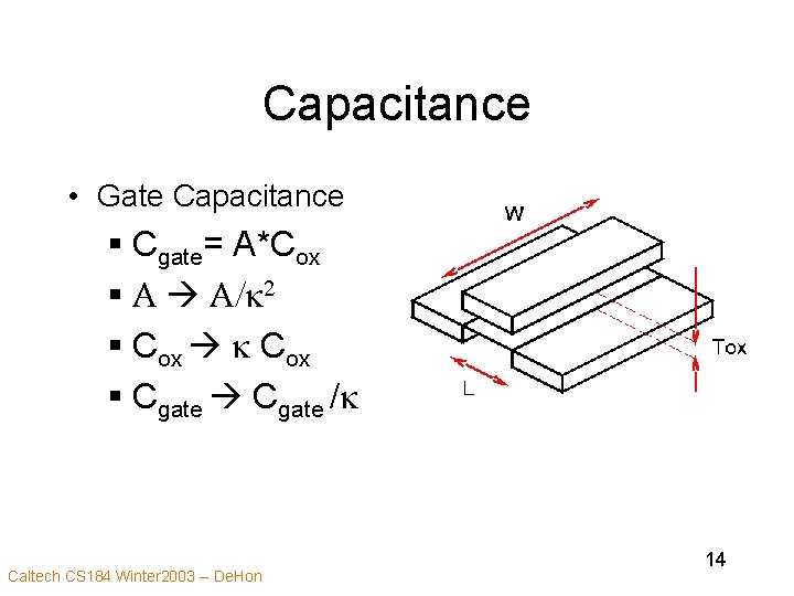
Capacitance • Gate Capacitance § Cgate= A*Cox § A A/k 2 § Cox k Cox § Cgate /k Caltech CS 184 Winter 2003 -- De. Hon 14

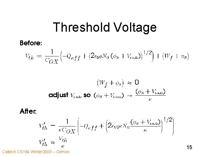
Threshold Voltage Caltech CS 184 Winter 2003 -- De. Hon 15

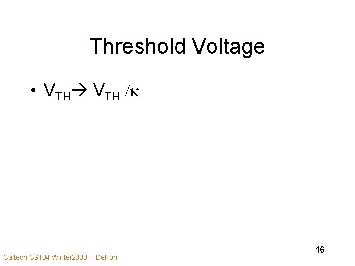
Threshold Voltage • VTH /k Caltech CS 184 Winter 2003 -- De. Hon 16

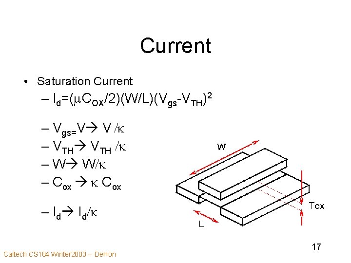
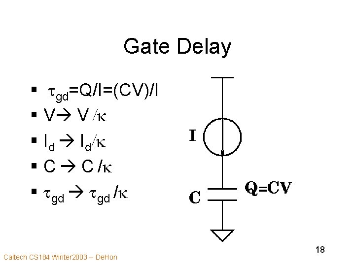
Current • Saturation Current – Id=(m. COX/2)(W/L)(Vgs-VTH)2 – Vgs=V V /k – VTH /k – W W/k – Cox k Cox – Id Id/k Caltech CS 184 Winter 2003 -- De. Hon 17

Gate Delay § tgd=Q/I=(CV)/I § V V /k § Id Id/k § C C /k § tgd /k Caltech CS 184 Winter 2003 -- De. Hon 18

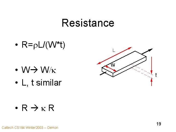
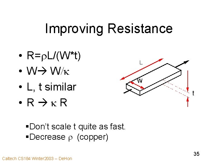
Resistance • R=r. L/(W*t) • W W/k • L, t similar • R k R Caltech CS 184 Winter 2003 -- De. Hon 19

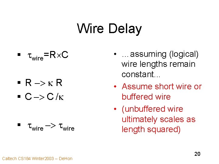
Wire Delay § twire=R C § R -> k R § C -> C /k § twire -> twire Caltech CS 184 Winter 2003 -- De. Hon • …assuming (logical) wire lengths remain constant. . . • Assume short wire or buffered wire • (unbuffered wire ultimately scales as length squared) 20

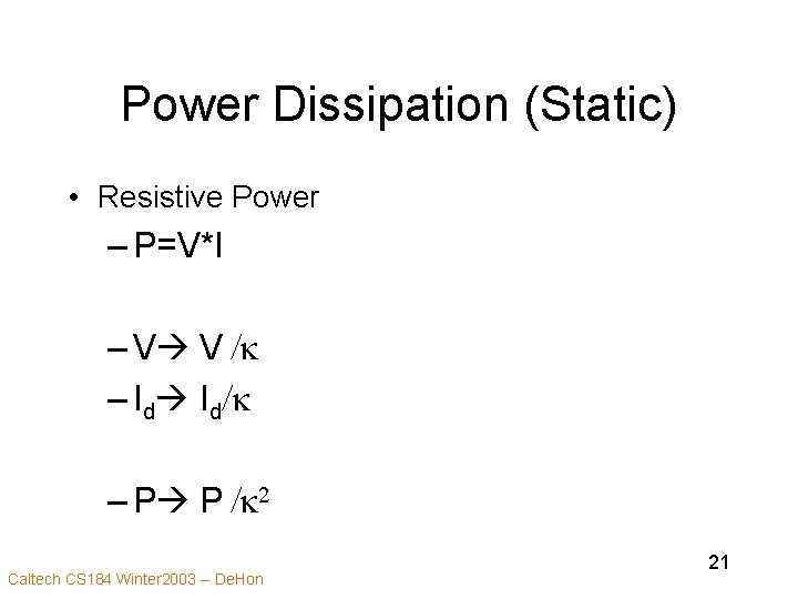
Power Dissipation (Static) • Resistive Power – P=V*I – V V /k – Id Id/k – P P /k 2 Caltech CS 184 Winter 2003 -- De. Hon 21

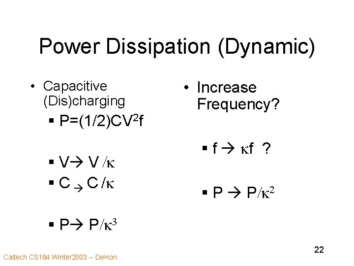
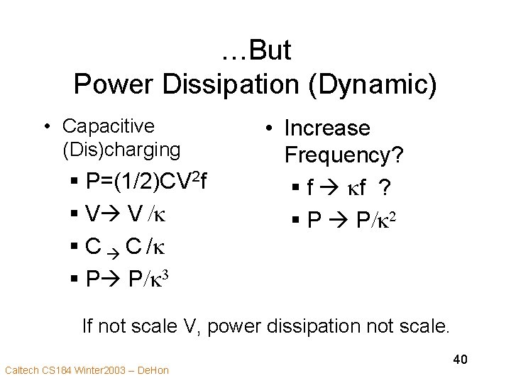
Power Dissipation (Dynamic) • Capacitive (Dis)charging § P=(1/2)CV 2 f § V V /k § C C /k • Increase Frequency? § f kf ? § P P/k 2 § P P/k 3 Caltech CS 184 Winter 2003 -- De. Hon 22

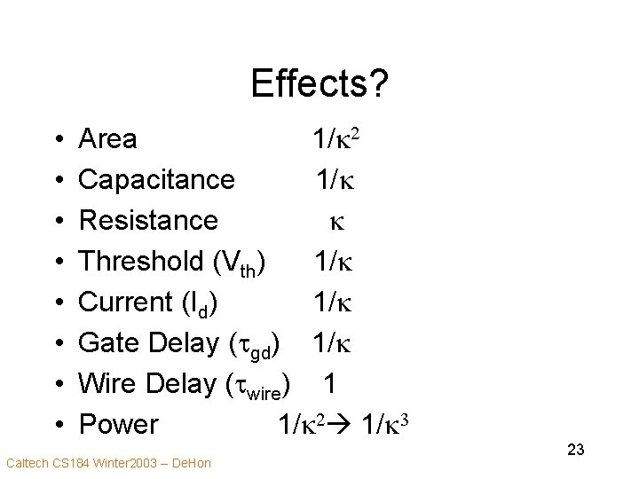
Effects? • • Area 1/k 2 Capacitance 1/k Resistance k Threshold (Vth) 1/k Current (Id) 1/k Gate Delay (tgd) 1/k Wire Delay (twire) 1 Power 1/k 2 1/k 3 Caltech CS 184 Winter 2003 -- De. Hon 23

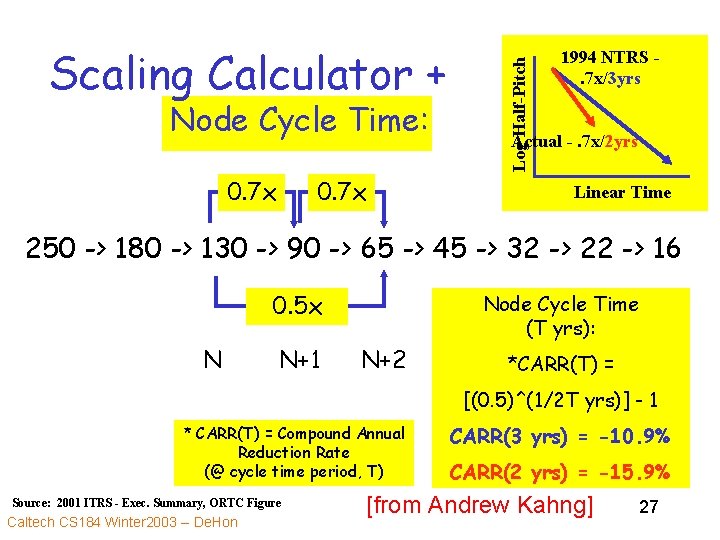
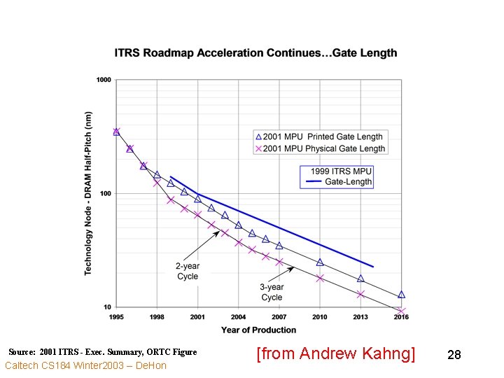
ITRS Roadmap • Semiconductor Industry rides this scaling curve • Try to predict where industry going – (requirements…self fulfilling prophecy) • http: //public. itrs. net Caltech CS 184 Winter 2003 -- De. Hon 24
![MOS Transistor Scaling 1974 to present S0 7 0 5 x per 2 nodes MOS Transistor Scaling (1974 to present) S=0. 7 [0. 5 x per 2 nodes]](https://slidetodoc.com/presentation_image_h/c1d000d289ee05c5b6b9e41cc804ea33/image-25.jpg)
MOS Transistor Scaling (1974 to present) S=0. 7 [0. 5 x per 2 nodes] Pitch Source: 2001 ITRS - Exec. Summary, ORTC Figure Caltech CS 184 Winter 2003 -- De. Hon Gate [from Andrew Kahng] 25

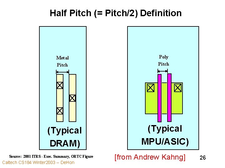
Half Pitch (= Pitch/2) Definition Metal Pitch (Typical DRAM) Source: 2001 ITRS - Exec. Summary, ORTC Figure Caltech CS 184 Winter 2003 -- De. Hon Poly Pitch (Typical MPU/ASIC) [from Andrew Kahng] 26

Node Cycle Time: 0. 7 x Log Half-Pitch Scaling Calculator + 1994 NTRS. 7 x/3 yrs Actual -. 7 x/2 yrs Linear Time 250 -> 180 -> 130 -> 90 -> 65 -> 45 -> 32 -> 22 -> 16 0. 5 x N N+1 Node Cycle Time (T yrs): N+2 *CARR(T) = [(0. 5)^(1/2 T yrs)] - 1 * CARR(T) = Compound Annual Reduction Rate (@ cycle time period, T) Source: 2001 ITRS - Exec. Summary, ORTC Figure Caltech CS 184 Winter 2003 -- De. Hon CARR(3 yrs) = -10. 9% CARR(2 yrs) = -15. 9% [from Andrew Kahng] 27

Source: 2001 ITRS - Exec. Summary, ORTC Figure Caltech CS 184 Winter 2003 -- De. Hon [from Andrew Kahng] 28

Delays? • If delays in gates/switching? • If delays in interconnect? • Logical interconnect lengths? Caltech CS 184 Winter 2003 -- De. Hon 29
![Delays If delays in gatesswitching Delay reduce with 1k l Caltech CS Delays? • If delays in gates/switching? – Delay reduce with 1/k [l] Caltech CS](https://slidetodoc.com/presentation_image_h/c1d000d289ee05c5b6b9e41cc804ea33/image-30.jpg)
Delays? • If delays in gates/switching? – Delay reduce with 1/k [l] Caltech CS 184 Winter 2003 -- De. Hon 30

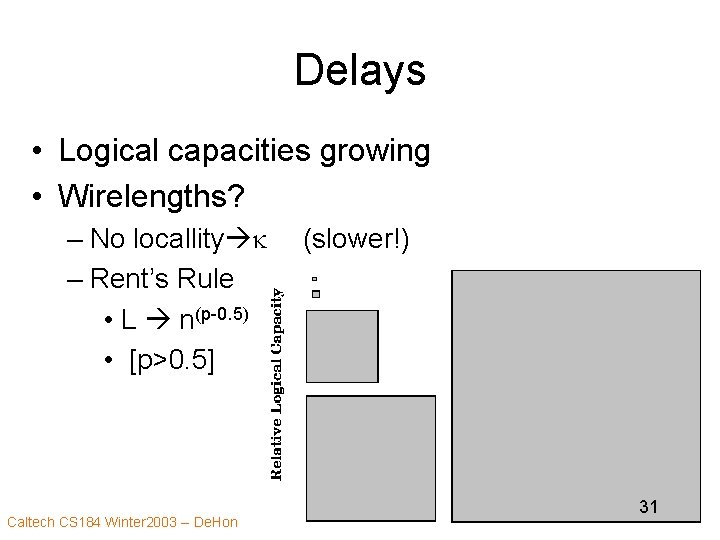
Delays • Logical capacities growing • Wirelengths? – No locallity k – Rent’s Rule • L n(p-0. 5) • [p>0. 5] Caltech CS 184 Winter 2003 -- De. Hon (slower!) 31

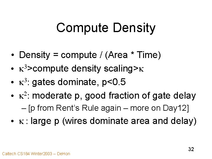
Compute Density • • Density = compute / (Area * Time) k 3>compute density scaling>k k 3: gates dominate, p<0. 5 k 2: moderate p, good fraction of gate delay – [p from Rent’s Rule again – more on Day 12] • k : large p (wires dominate area and delay) Caltech CS 184 Winter 2003 -- De. Hon 32

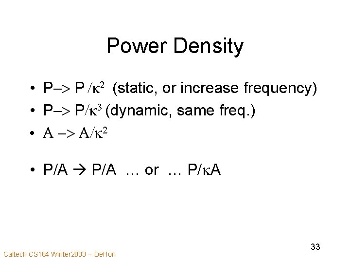
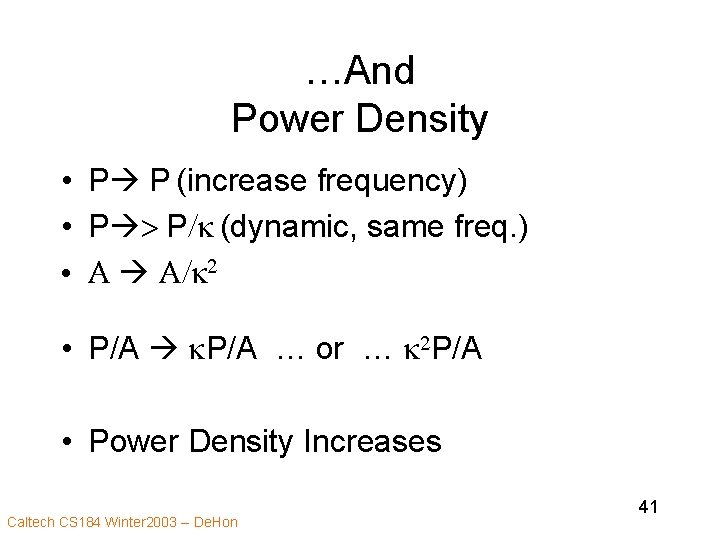
Power Density • P-> P /k 2 (static, or increase frequency) • P-> P/k 3 (dynamic, same freq. ) • A -> A/k 2 • P/A … or … P/k. A Caltech CS 184 Winter 2003 -- De. Hon 33

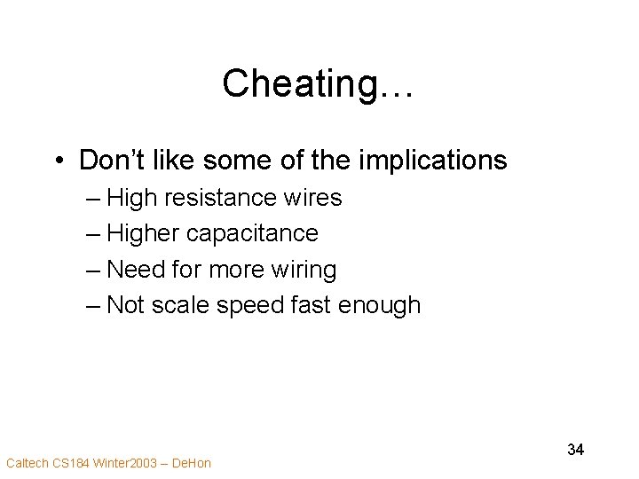
Cheating… • Don’t like some of the implications – High resistance wires – Higher capacitance – Need for more wiring – Not scale speed fast enough Caltech CS 184 Winter 2003 -- De. Hon 34

Improving Resistance • • R=r. L/(W*t) W W/k L, t similar R k R §Don’t scale t quite as fast. §Decrease r (copper) Caltech CS 184 Winter 2003 -- De. Hon 35

Improving Capacitance • Capacitance per unit area – Cox= e. Si. O 2/Tox – Tox/k – Cox k Cox Reduce Dielectric Constant e Caltech CS 184 Winter 2003 -- De. Hon 36

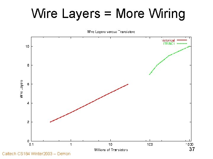
Wire Layers = More Wiring Caltech CS 184 Winter 2003 -- De. Hon 37

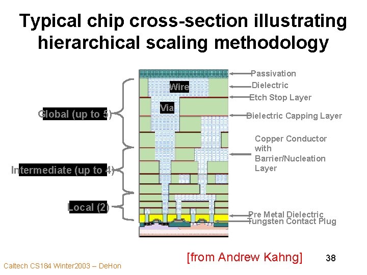
Typical chip cross-section illustrating hierarchical scaling methodology Wire Global (up to 5) Intermediate (up to 4) Local (2) Caltech CS 184 Winter 2003 -- De. Hon Via Passivation Dielectric Etch Stop Layer Dielectric Capping Layer Copper Conductor with Barrier/Nucleation Layer Pre Metal Dielectric Tungsten Contact Plug [from Andrew Kahng] 38

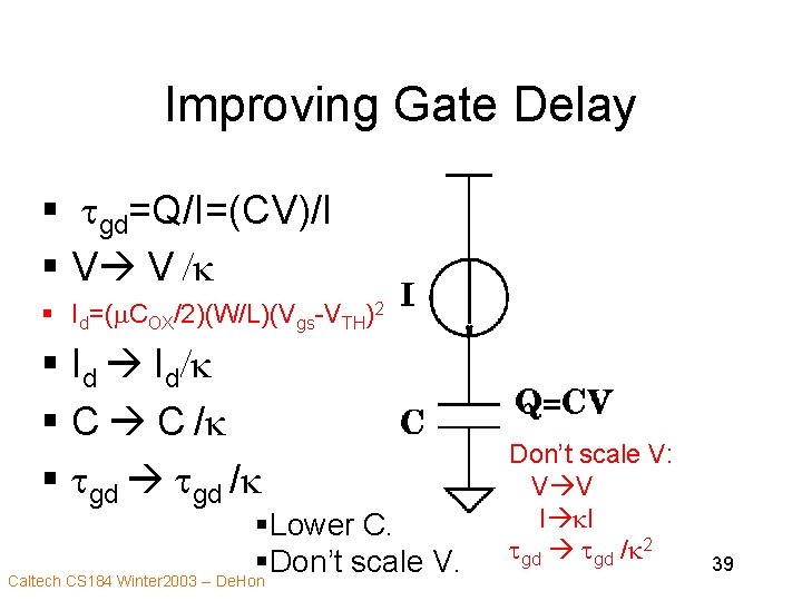
Improving Gate Delay § tgd=Q/I=(CV)/I § V V /k § Id=(m. COX/2)(W/L)(Vgs-VTH)2 § Id Id/k § C C /k § tgd /k §Lower C. §Don’t scale V. Caltech CS 184 Winter 2003 -- De. Hon Don’t scale V: V V I k. I tgd /k 2 39

…But Power Dissipation (Dynamic) • Capacitive (Dis)charging § P=(1/2)CV 2 f § V V /k § C C /k § P P/k 3 • Increase Frequency? § f kf ? § P P/k 2 If not scale V, power dissipation not scale. Caltech CS 184 Winter 2003 -- De. Hon 40

…And Power Density • P P (increase frequency) • P > P/k (dynamic, same freq. ) • A A/k 2 • P/A k. P/A … or … k 2 P/A • Power Density Increases Caltech CS 184 Winter 2003 -- De. Hon 41

Physical Limits • Doping? • Features? Caltech CS 184 Winter 2003 -- De. Hon 42

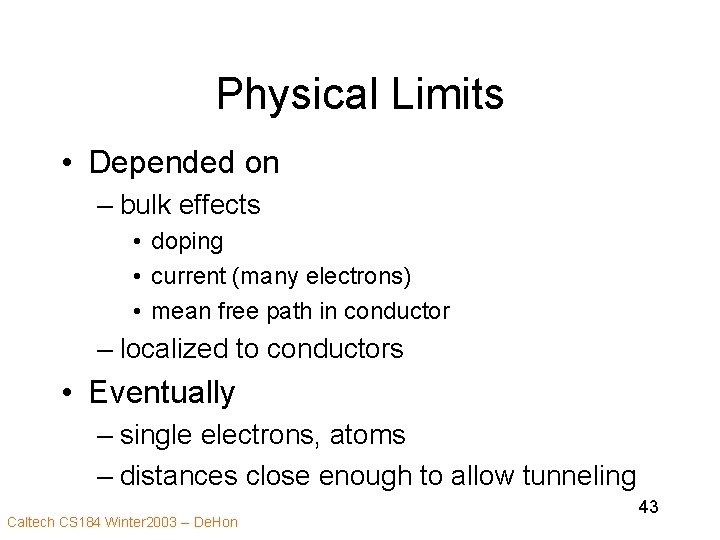
Physical Limits • Depended on – bulk effects • doping • current (many electrons) • mean free path in conductor – localized to conductors • Eventually – single electrons, atoms – distances close enough to allow tunneling Caltech CS 184 Winter 2003 -- De. Hon 43

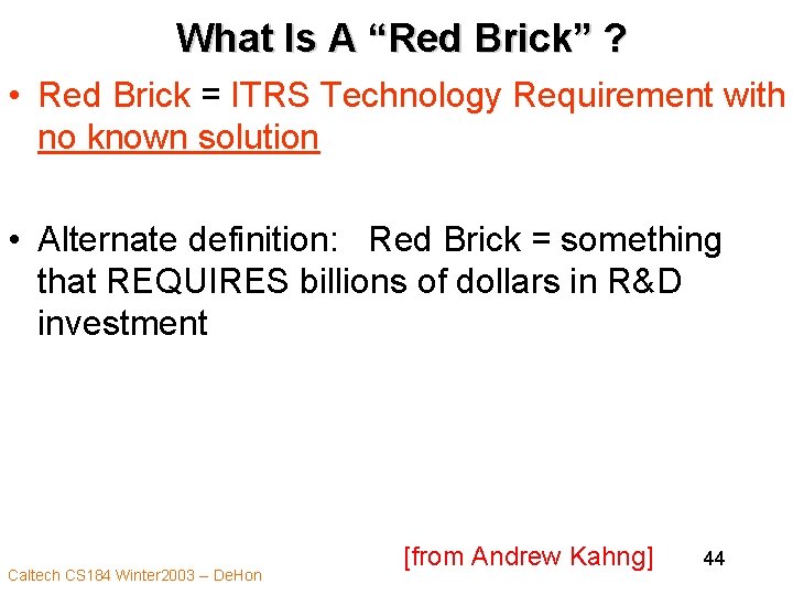
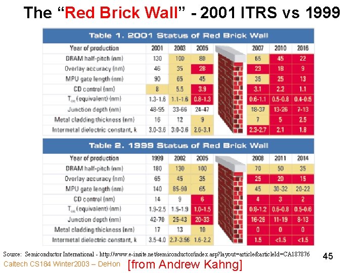
What Is A “Red Brick” ? • Red Brick = ITRS Technology Requirement with no known solution • Alternate definition: Red Brick = something that REQUIRES billions of dollars in R&D investment Caltech CS 184 Winter 2003 -- De. Hon [from Andrew Kahng] 44

The “Red Brick Wall” - 2001 ITRS vs 1999 Source: Semiconductor International - http: //www. e-insite. net/semiconductor/index. asp? layout =article&article. Id=CA 187876 Caltech CS 184 Winter 2003 -- De. Hon [from Andrew Kahng] 45

Finishing Up. . . Caltech CS 184 Winter 2003 -- De. Hon 46
![Big Ideas MSB Ideas Moderately predictable VLSI Scaling unprecedented capacitiescapability growth for Big Ideas [MSB Ideas] • Moderately predictable VLSI Scaling – unprecedented capacities/capability growth for](https://slidetodoc.com/presentation_image_h/c1d000d289ee05c5b6b9e41cc804ea33/image-47.jpg)
Big Ideas [MSB Ideas] • Moderately predictable VLSI Scaling – unprecedented capacities/capability growth for engineered systems – change – be prepared to exploit – account for in comparing across time Caltech CS 184 Winter 2003 -- De. Hon 47
![Big Ideas MSB1 Ideas Uniform scaling reasonably accurate for past couple of decades Big Ideas [MSB-1 Ideas] • Uniform scaling reasonably accurate for past couple of decades](https://slidetodoc.com/presentation_image_h/c1d000d289ee05c5b6b9e41cc804ea33/image-48.jpg)
Big Ideas [MSB-1 Ideas] • Uniform scaling reasonably accurate for past couple of decades • Area increase k 2 – Real capacity maybe a little less? • Gate delay decreases (1/k) • Wire delay not decrease, maybe increase • Overall delay decrease less than (1/k) Caltech CS 184 Winter 2003 -- De. Hon 48