CIS 501 Computer Architecture Unit 3 Technology Energy
- Slides: 55

CIS 501: Computer Architecture Unit 3: Technology & Energy Slides developed by Joe Devietti, Milo Martin & Amir Roth at UPenn with sources that included University of Wisconsin slides by Mark Hill, Guri Sohi, Jim Smith, and David Wood CIS 501: Comp. Arch. | Prof. Joe Devietti | Technology & Energy 1

This Unit: Technology & Energy • Technology basis • Fabrication (manufacturing) & cost • Transistors & wires • Implications of transistor scaling (Moore’s Law) • Energy & power CIS 501: Comp. Arch. | Prof. Joe Devietti | Technology & Energy 2

Technology & Fabrication CIS 501: Comp. Arch. | Prof. Joe Devietti | Technology & Energy 3

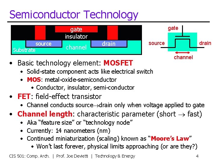
Semiconductor Technology gate insulator Substrate source channel gate drain source • Basic technology element: MOSFET drain channel • Solid-state component acts like electrical switch • MOS: metal-oxide-semiconductor • Conductor, insulator, semi-conductor • FET: field-effect transistor • Channel conducts source drain only when voltage applied to gate • Channel length: characteristic parameter (short fast) • Aka “feature size” or “technology node” • Currently: 14 nanometers (nm) • Continued miniaturization (scaling) known as “Moore’s Law” • Won’t last forever, physical limits approaching (or are they? ) CIS 501: Comp. Arch. | Prof. Joe Devietti | Technology & Energy 4

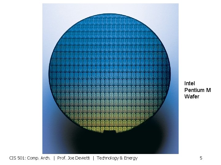
Intel Pentium M Wafer CIS 501: Comp. Arch. | Prof. Joe Devietti | Technology & Energy 5

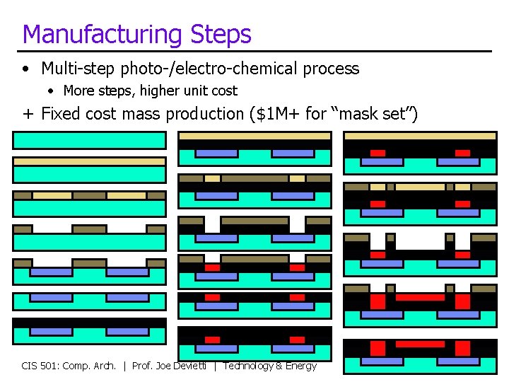
Manufacturing Steps • Multi-step photo-/electro-chemical process • More steps, higher unit cost + Fixed cost mass production ($1 M+ for “mask set”) CIS 501: Comp. Arch. | Prof. Joe Devietti | Technology & Energy 6

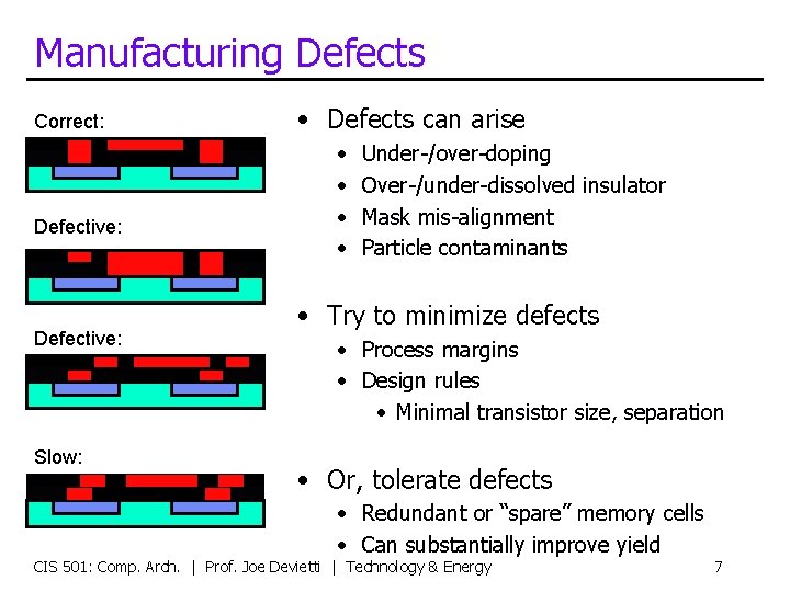
Manufacturing Defects Correct: Defective: Slow: • Defects can arise • • Under-/over-doping Over-/under-dissolved insulator Mask mis-alignment Particle contaminants • Try to minimize defects • Process margins • Design rules • Minimal transistor size, separation • Or, tolerate defects • Redundant or “spare” memory cells • Can substantially improve yield CIS 501: Comp. Arch. | Prof. Joe Devietti | Technology & Energy 7

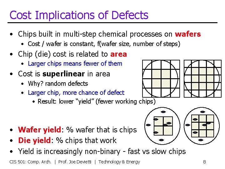
Cost Implications of Defects • Chips built in multi-step chemical processes on wafers • Cost / wafer is constant, f(wafer size, number of steps) • Chip (die) cost is related to area • Larger chips means fewer of them • Cost is superlinear in area • Why? random defects • Larger chip, more chance of defect • Result: lower “yield” (fewer working chips) • Wafer yield: % wafer that is chips • Die yield: % chips that work • Yield is increasingly non-binary - fast vs slow chips CIS 501: Comp. Arch. | Prof. Joe Devietti | Technology & Energy 8

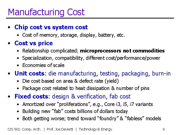
Manufacturing Cost • Chip cost vs system cost • Cost of memory, storage, display, battery, etc. • Cost vs price • Relationship complicated; microprocessors not commodities • Specialization, compatibility, different cost/performance/power • Economies of scale • Unit costs: die manufacturing, testing, packaging, burn-in • Die cost based on area & defect rate (yield) • Package cost related to heat dissipation & number of pins • Fixed costs: design & verification, fab cost • Amortized over “proliferations”, e. g. , Core i 3, i 5, i 7 variants • Building new “fab” costs billions of dollars today • Both getting worse; trend toward “foundry” & “fabless” models CIS 501: Comp. Arch. | Prof. Joe Devietti | Technology & Energy 9

Transistor Switching Speed CIS 501: Comp. Arch. | Prof. Joe Devietti | Technology & Energy 10

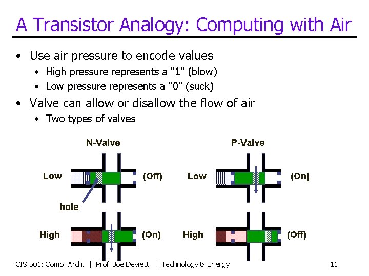
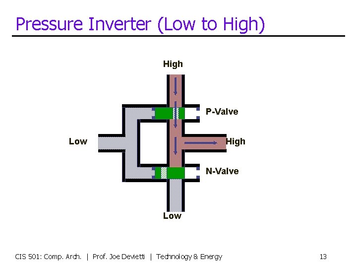
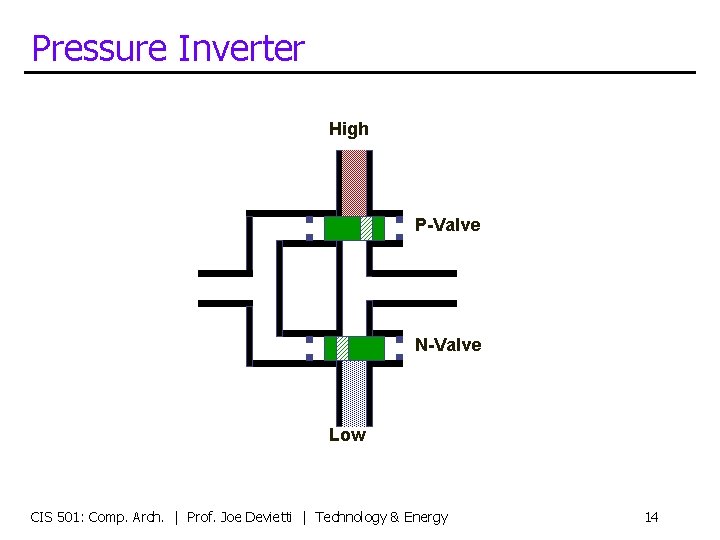
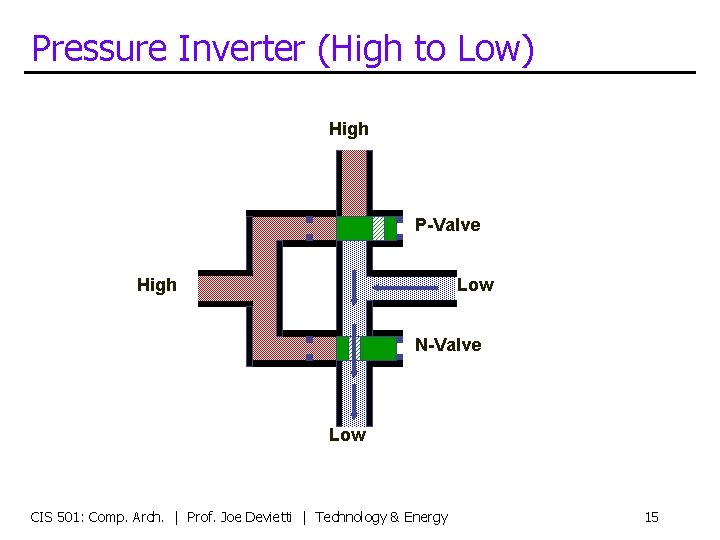
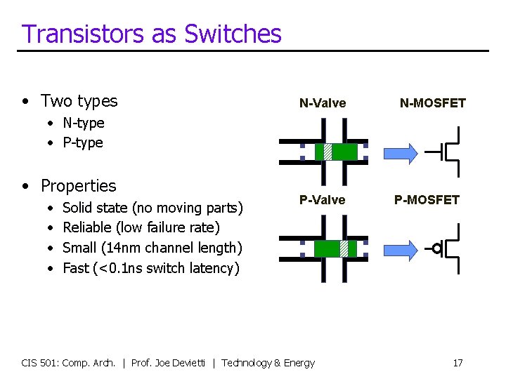
A Transistor Analogy: Computing with Air • Use air pressure to encode values • High pressure represents a “ 1” (blow) • Low pressure represents a “ 0” (suck) • Valve can allow or disallow the flow of air • Two types of valves N-Valve Low P-Valve (Off) Low (On) High (On) hole High CIS 501: Comp. Arch. | Prof. Joe Devietti | Technology & Energy (Off) 11

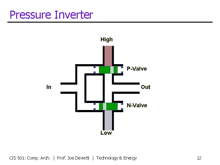
Pressure Inverter High P-Valve In Out N-Valve Low CIS 501: Comp. Arch. | Prof. Joe Devietti | Technology & Energy 12

Pressure Inverter (Low to High) High P-Valve High Low N-Valve Low CIS 501: Comp. Arch. | Prof. Joe Devietti | Technology & Energy 13

Pressure Inverter High P-Valve N-Valve Low CIS 501: Comp. Arch. | Prof. Joe Devietti | Technology & Energy 14

Pressure Inverter (High to Low) High P-Valve Low High N-Valve Low CIS 501: Comp. Arch. | Prof. Joe Devietti | Technology & Energy 15

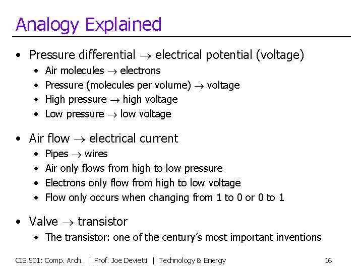
Analogy Explained • Pressure differential electrical potential (voltage) • • Air molecules electrons Pressure (molecules per volume) voltage High pressure high voltage Low pressure low voltage • Air flow electrical current • • Pipes wires Air only flows from high to low pressure Electrons only flow from high to low voltage Flow only occurs when changing from 1 to 0 or 0 to 1 • Valve transistor • The transistor: one of the century’s most important inventions CIS 501: Comp. Arch. | Prof. Joe Devietti | Technology & Energy 16

Transistors as Switches • Two types N-Valve N-MOSFET • N-type • P-type • Properties • • Solid state (no moving parts) Reliable (low failure rate) Small (14 nm channel length) Fast (<0. 1 ns switch latency) P-Valve CIS 501: Comp. Arch. | Prof. Joe Devietti | Technology & Energy P-MOSFET 17

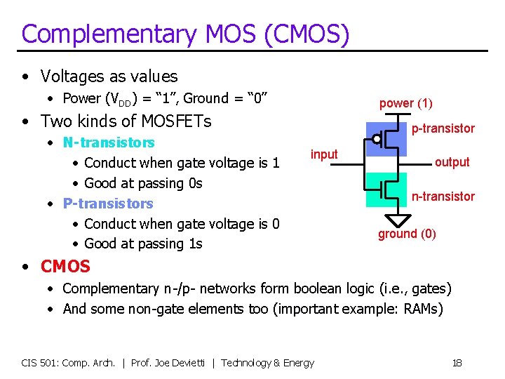
Complementary MOS (CMOS) • Voltages as values • Power (VDD) = “ 1”, Ground = “ 0” power (1) • Two kinds of MOSFETs • N-transistors • Conduct when gate voltage is 1 • Good at passing 0 s • P-transistors • Conduct when gate voltage is 0 • Good at passing 1 s p-transistor input output n-transistor ground (0) • CMOS • Complementary n-/p- networks form boolean logic (i. e. , gates) • And some non-gate elements too (important example: RAMs) CIS 501: Comp. Arch. | Prof. Joe Devietti | Technology & Energy 18

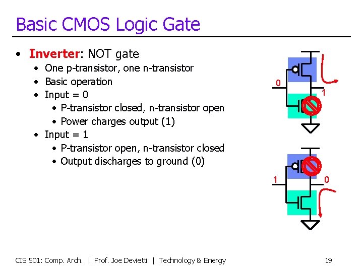
Basic CMOS Logic Gate • Inverter: NOT gate • One p-transistor, one n-transistor • Basic operation • Input = 0 • P-transistor closed, n-transistor open • Power charges output (1) • Input = 1 • P-transistor open, n-transistor closed • Output discharges to ground (0) 0 1 CIS 501: Comp. Arch. | Prof. Joe Devietti | Technology & Energy 1 0 19

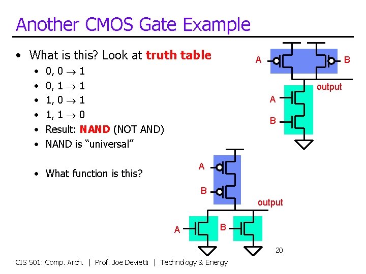
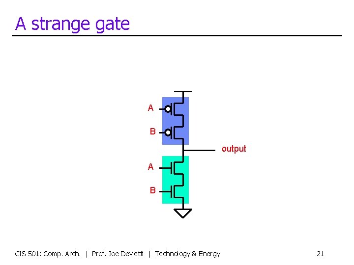
Another CMOS Gate Example • What is this? Look at truth table • • • A 0, 0 1 0, 1 1 1, 0 1 1, 1 0 Result: NAND (NOT AND) NAND is “universal” B output A B A • What function is this? B output A B 20 CIS 501: Comp. Arch. | Prof. Joe Devietti | Technology & Energy

A strange gate A B output A B CIS 501: Comp. Arch. | Prof. Joe Devietti | Technology & Energy 21

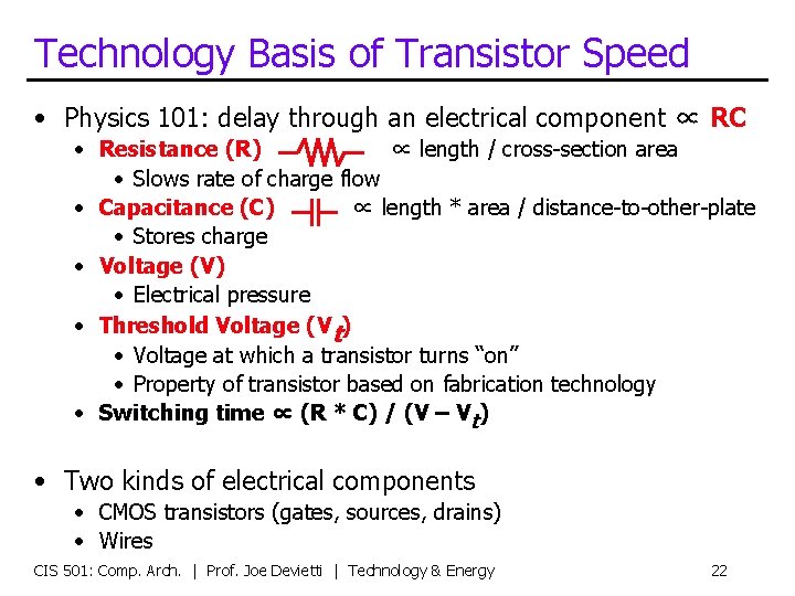
Technology Basis of Transistor Speed • Physics 101: delay through an electrical component ∝ RC • Resistance (R) ∝ length / cross-section area • Slows rate of charge flow • Capacitance (C) ∝ length * area / distance-to-other-plate • Stores charge • Voltage (V) • Electrical pressure • Threshold Voltage (Vt) • Voltage at which a transistor turns “on” • Property of transistor based on fabrication technology • Switching time ∝ (R * C) / (V – Vt) • Two kinds of electrical components • CMOS transistors (gates, sources, drains) • Wires CIS 501: Comp. Arch. | Prof. Joe Devietti | Technology & Energy 22

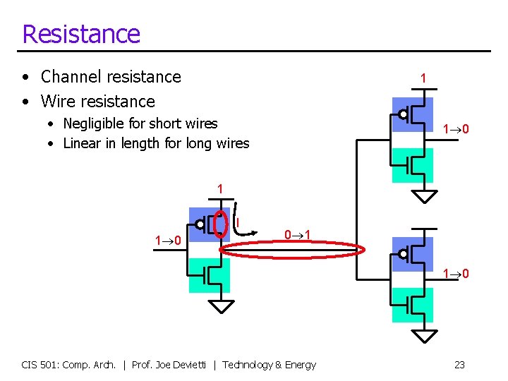
Resistance • Channel resistance • Wire resistance 1 • Negligible for short wires • Linear in length for long wires 1 0 1 I 1 0 0 1 1 0 CIS 501: Comp. Arch. | Prof. Joe Devietti | Technology & Energy 23

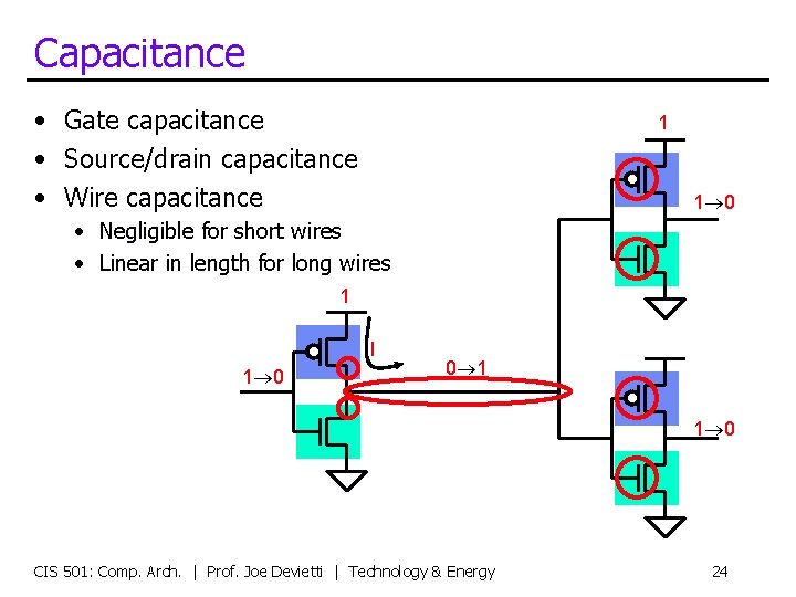
Capacitance • Gate capacitance • Source/drain capacitance • Wire capacitance 1 1 0 • Negligible for short wires • Linear in length for long wires 1 I 1 0 0 1 1 0 CIS 501: Comp. Arch. | Prof. Joe Devietti | Technology & Energy 24

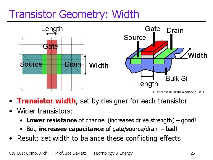
Transistor Geometry: Width Length Gate Drain Source Gate Width Source Drain Width Length Bulk Si Diagrams © Krste Asanovic, MIT • Transistor width, set by designer for each transistor • Wider transistors: • Lower resistance of channel (increases drive strength) – good! • But, increases capacitance of gate/source/drain – bad! • Result: set width to balance these conflicting effects CIS 501: Comp. Arch. | Prof. Joe Devietti | Technology & Energy 25

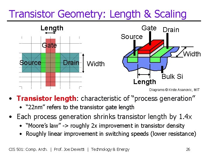
Transistor Geometry: Length & Scaling Length Gate Drain Source Gate Width Source Drain Width Length Bulk Si Diagrams © Krste Asanovic, MIT • Transistor length: characteristic of “process generation” • “ 22 nm” refers to the transistor gate length • Each process generation shrinks transistor length by 1. 4 x • “Moore’s law” -> roughly 2 x improvement in transistor density • Roughly linear improvement in switching speeds (lower resistance) CIS 501: Comp. Arch. | Prof. Joe Devietti | Technology & Energy 26

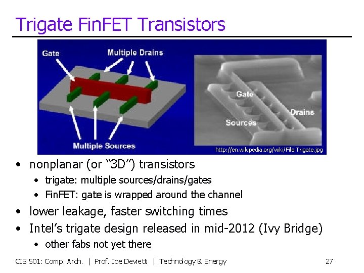
Trigate Fin. FET Transistors http: //en. wikipedia. org/wiki/File: Trigate. jpg • nonplanar (or “ 3 D”) transistors • trigate: multiple sources/drains/gates • Fin. FET: gate is wrapped around the channel • lower leakage, faster switching times • Intel’s trigate design released in mid-2012 (Ivy Bridge) • other fabs not yet there CIS 501: Comp. Arch. | Prof. Joe Devietti | Technology & Energy 27

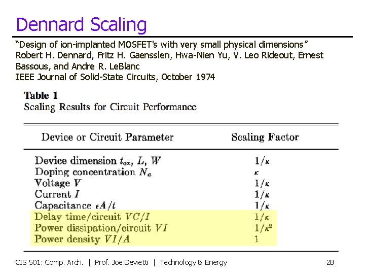
Dennard Scaling “Design of ion-implanted MOSFET's with very small physical dimensions” Robert H. Dennard, Fritz H. Gaensslen, Hwa-Nien Yu, V. Leo Rideout, Ernest Bassous, and Andre R. Le. Blanc IEEE Journal of Solid-State Circuits, October 1974 CIS 501: Comp. Arch. | Prof. Joe Devietti | Technology & Energy 28

Dennard Scaling • stopped in ~2005 due to leakage • V close to Vt, transistors never really “on” or “off” • gate-oxide leakage due to very small oxide thickness • quantum-mechanical electron tunneling • Moore’s Law still in effect! • but power usage goes up with increasing transistor counts CIS 501: Comp. Arch. | Prof. Joe Devietti | Technology & Energy 29

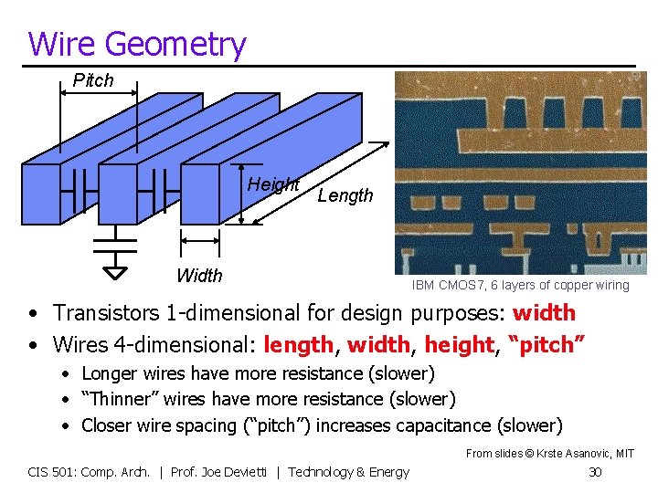
Wire Geometry Pitch Height Length Width IBM CMOS 7, 6 layers of copper wiring • Transistors 1 -dimensional for design purposes: width • Wires 4 -dimensional: length, width, height, “pitch” • Longer wires have more resistance (slower) • “Thinner” wires have more resistance (slower) • Closer wire spacing (“pitch”) increases capacitance (slower) From slides © Krste Asanovic, MIT CIS 501: Comp. Arch. | Prof. Joe Devietti | Technology & Energy 30

Increasing Problem: Wire Delay • RC Delay of wires • Resistance proportional to: resistivity * length / (cross section) • Wires with smaller cross section have higher resistance • Resistivity (type of metal, copper vs aluminum) • Capacitance proportional to length • And wire spacing (closer wires have large capacitance) • Permittivity or “dielectric constant” (of material between wires) • Result: delay of a wire is quadratic in length • Insert “inverter” repeaters for long wires • Why? To bring it back to linear delay… but repeaters still add delay • Long wires are relatively slow compared to transistors • And take a relatively longer time to cross relatively larger chips CIS 501: Comp. Arch. | Prof. Joe Devietti | Technology & Energy 31

Technology Scaling Trends CIS 501: Comp. Arch. | Prof. Joe Devietti | Technology & Energy 32

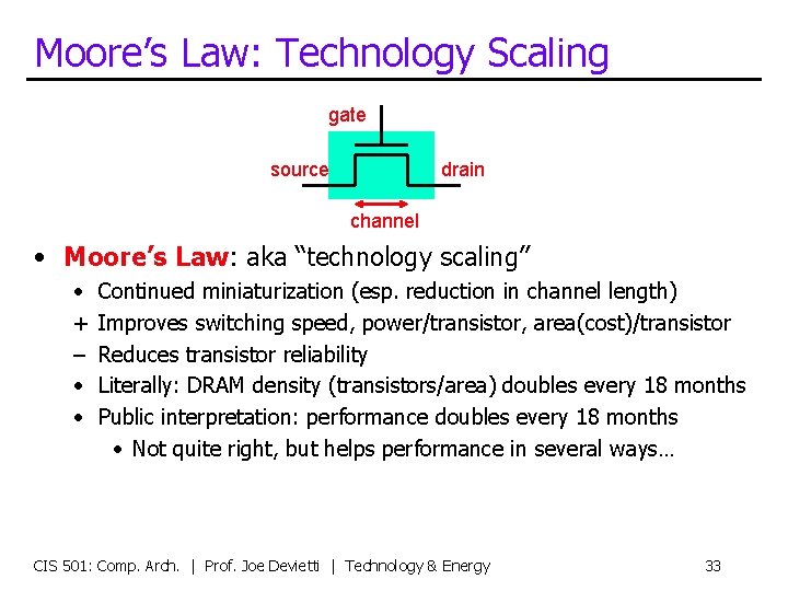
Moore’s Law: Technology Scaling gate source drain channel • Moore’s Law: aka “technology scaling” • + – • • Continued miniaturization (esp. reduction in channel length) Improves switching speed, power/transistor, area(cost)/transistor Reduces transistor reliability Literally: DRAM density (transistors/area) doubles every 18 months Public interpretation: performance doubles every 18 months • Not quite right, but helps performance in several ways… CIS 501: Comp. Arch. | Prof. Joe Devietti | Technology & Energy 33

Moore’s Effect #1: Transistor Count • Linear shrink in each dimension • 180 nm, 130 nm, 90 nm, 65 nm, 45 nm, 32 nm, 22 nm, 14 nm, … • Each generation is a 0. 7 x linear shrink • older generation was 1. 414 x larger • Shrink each dimension (2 D) • Results in 2 x more transistors (1. 414*1. 414) per area • Generally reduces cost per transistor • More transistors can increase performance • Job of a computer architect: use the ever-increasing number of transistors • Today, desktop/laptop processor chips have 1 B+ transistors CIS 501: Comp. Arch. | Prof. Joe Devietti | Technology & Energy 34

Moore’s Effect #2: RC Delay • First-order: speed scales proportional to gate length • Has provided much of the performance gains in the past • Scaling helps wire and gate delays in some ways… + Transistors become shorter (Resistance ), narrower (Capacitance ) + Wires become shorter (Length Resistance ) + Wire “surface areas” become smaller (Capacitance ) • Hurts in others… – Transistors become narrower (Resistance ) – Gate insulator thickness becomes smaller (Capacitance ) – Wires becomes thinner (Resistance ) • What to do? • Take the good, use wire/transistor sizing to counter the bad • Exploit new materials: Aluminum Copper, metal gate, high-K CIS 501: Comp. Arch. | Prof. Joe Devietti | Technology & Energy 35

Moore’s Effect #3: Cost • Mixed impact on unit integrated circuit cost + Either lower cost for same functionality… + Or same cost for more functionality – Difficult to achieve high yields – Increases startup cost • More expensive fabrication equipment • Takes longer to design, verify, and test chips – Process variation across chip increasing • Some transistors slow, some fast • Increasingly active research area: dealing with this problem CIS 501: Comp. Arch. | Prof. Joe Devietti | Technology & Energy 36

Moore’s Effect #4: Psychological • Moore’s Curve: common interpretation of Moore’s Law • “CPU performance doubles every 18 months” • Self fulfilling prophecy: 2 X every 18 months is ~1% per week • Q: Would you add a feature that improved performance 20% if it would delay the chip 8 months? • Processors under Moore’s Curve (arrive too late) fail spectacularly • E. g. , Intel’s Itanium, Sun’s Millennium CIS 501: Comp. Arch. | Prof. Joe Devietti | Technology & Energy 37

Moore’s Law in the Future • Won’t last forever, approaching physical limits • “If something must eventually stop, it can’t go on forever” • But betting against it has proved foolish in the past • Perhaps will “slow” rather than stop abruptly • Transistor count will likely continue to scale • 3 D “die stacking” is arriving • But transistor performance scaling? • Running into physical limits • Example: gate oxide <10 silicon atoms! • Can’t decrease it much further • Power is becoming the limiting factor CIS 501: Comp. Arch. | Prof. Joe Devietti | Technology & Energy 38

Power & Energy CIS 501: Comp. Arch. | Prof. Joe Devietti | Technology & Energy 39

Power/Energy Are Increasingly Important • Battery life for mobile devices • Laptops, phones, cameras • Tolerable temperature for devices without active cooling • Power means temperature, active cooling means cost • No room for a fan in a cell phone, no market for a hot cell phone • Electric bill for compute/data centers • Pay for power twice: once in, once out (to cool) • Environmental concerns • IT accounts for growing fraction of electricity consumption CIS 501: Comp. Arch. | Prof. Joe Devietti | Technology & Energy 40

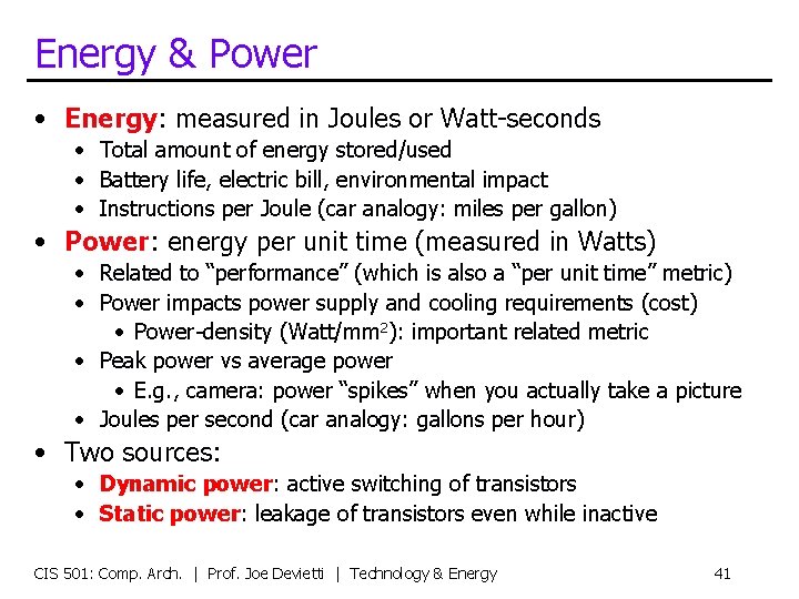
Energy & Power • Energy: measured in Joules or Watt-seconds • Total amount of energy stored/used • Battery life, electric bill, environmental impact • Instructions per Joule (car analogy: miles per gallon) • Power: energy per unit time (measured in Watts) • Related to “performance” (which is also a “per unit time” metric) • Power impacts power supply and cooling requirements (cost) • Power-density (Watt/mm 2): important related metric • Peak power vs average power • E. g. , camera: power “spikes” when you actually take a picture • Joules per second (car analogy: gallons per hour) • Two sources: • Dynamic power: active switching of transistors • Static power: leakage of transistors even while inactive CIS 501: Comp. Arch. | Prof. Joe Devietti | Technology & Energy 41

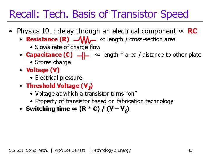
Recall: Tech. Basis of Transistor Speed • Physics 101: delay through an electrical component ∝ RC • Resistance (R) ∝ length / cross-section area • Slows rate of charge flow • Capacitance (C) ∝ length * area / distance-to-other-plate • Stores charge • Voltage (V) • Electrical pressure • Threshold Voltage (Vt) • Voltage at which a transistor turns “on” • Property of transistor based on fabrication technology • Switching time ∝ (R * C) / (V – Vt) CIS 501: Comp. Arch. | Prof. Joe Devietti | Technology & Energy 42

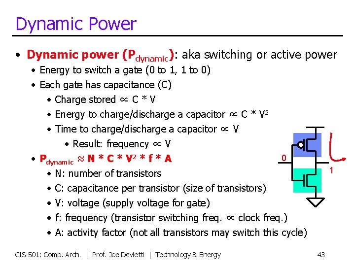
Dynamic Power • Dynamic power (Pdynamic): aka switching or active power • Energy to switch a gate (0 to 1, 1 to 0) • Each gate has capacitance (C) • Charge stored ∝ C * V • Energy to charge/discharge a capacitor ∝ C * V 2 • Time to charge/discharge a capacitor ∝ V • Result: frequency ∝ V 0 • Pdynamic ≈ N * C * V 2 * f * A • N: number of transistors • C: capacitance per transistor (size of transistors) • V: voltage (supply voltage for gate) • f: frequency (transistor switching freq. ∝ clock freq. ) • A: activity factor (not all transistors may switch this cycle) CIS 501: Comp. Arch. | Prof. Joe Devietti | Technology & Energy 1 43

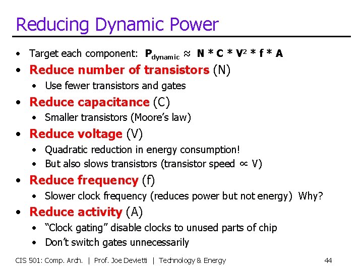
Reducing Dynamic Power • Target each component: Pdynamic ≈ N * C * V 2 * f * A • Reduce number of transistors (N) • Use fewer transistors and gates • Reduce capacitance (C) • Smaller transistors (Moore’s law) • Reduce voltage (V) • Quadratic reduction in energy consumption! • But also slows transistors (transistor speed ∝ V) • Reduce frequency (f) • Slower clock frequency (reduces power but not energy) Why? • Reduce activity (A) • “Clock gating” disable clocks to unused parts of chip • Don’t switch gates unnecessarily CIS 501: Comp. Arch. | Prof. Joe Devietti | Technology & Energy 44

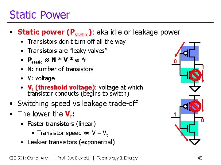
Static Power • Static power (Pstatic): aka idle or leakage power • • • Transistors don’t turn off all the way Transistors are “leaky valves” Pstatic ≈ N * V * e–Vt N: number of transistors V: voltage Vt (threshold voltage): voltage at which transistor conducts (begins to switch) • Switching speed vs leakage trade-off • The lower the Vt: • Faster transistors (linear) • Transistor speed ∝ V – Vt • Leakier transistors (exponential) CIS 501: Comp. Arch. | Prof. Joe Devietti | Technology & Energy 0 1 1 0 45

Reducing Static Power • Target each component: Pstatic ≈ N * V * e–Vt • Reduce number of transistors (N) • Use fewer transistors/gates • Disable transistors (also targets N) • • “Power gating” disable power to unused parts (long latency to power up) Power down units (or entire cores) not being used • Reduce voltage (V) • • Linear reduction in static energy consumption But also slows transistors (transistor speed ∝ V) • Dual Vt – use a mixture of high and low Vt transistors • • Use slow, low-leak transistors in SRAM arrays Requires extra fabrication steps (cost) • Low-leakage transistors • High-K/Metal-Gates in Intel’s 45 nm process, “tri-gate” in Intel’s 22 nm • Reducing frequency can hurt energy efficiency due to leakage power CIS 501: Comp. Arch. | Prof. Joe Devietti | Technology & Energy 46

Dynamic Voltage/Frequency Scaling • Dynamically trade-off power for performance • Change the voltage and frequency at runtime • Under control of operating system • Recall: Pdynamic ≈ N * C * V 2 * f * A • Because frequency ∝ to V – Vt… • Pdynamic ∝ to V 2(V – Vt) ≈ V 3 • Reduce both voltage and frequency linearly • Cubic decrease in dynamic power • Linear decrease in performance (actually sub-linear) • Thus, only about quadratic decrease in energy • Linear decrease in static power • Thus, static energy can become dominant • Newer chips can adjust frequency on a per-core basis CIS 501: Comp. Arch. | Prof. Joe Devietti | Technology & Energy 47

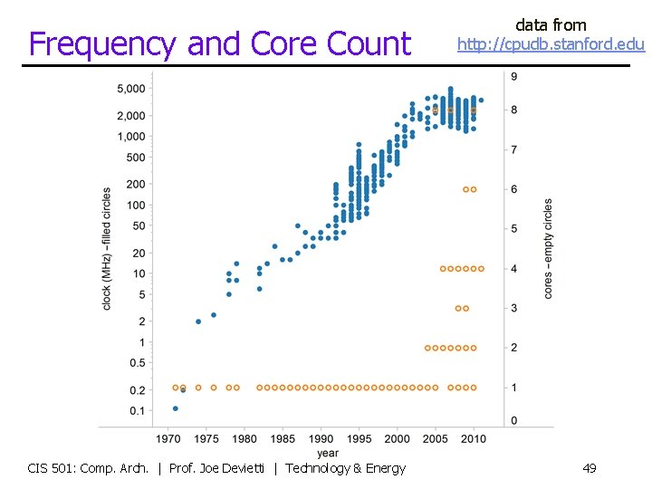
Frequency and Core Count CIS 501: Comp. Arch. | Prof. Joe Devietti | Technology & Energy data from http: //cpudb. stanford. edu 49

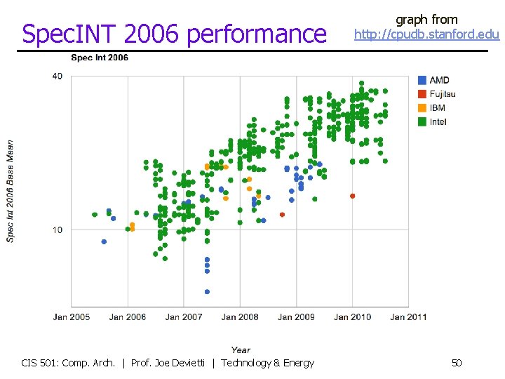
Spec. INT 2006 performance CIS 501: Comp. Arch. | Prof. Joe Devietti | Technology & Energy graph from http: //cpudb. stanford. edu 50

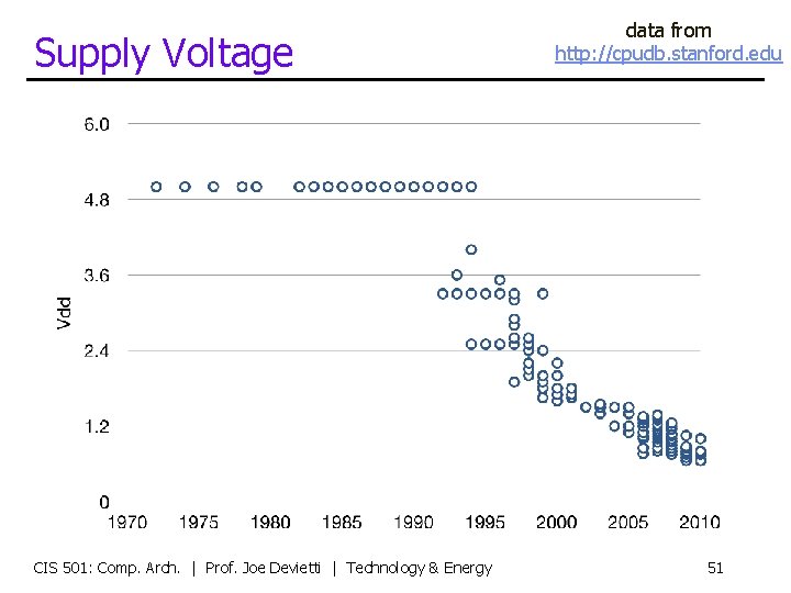
Supply Voltage CIS 501: Comp. Arch. | Prof. Joe Devietti | Technology & Energy data from http: //cpudb. stanford. edu 51

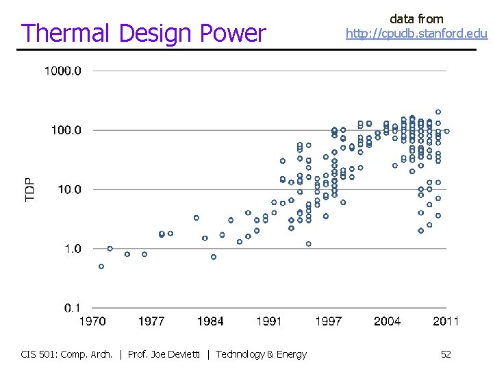
Thermal Design Power CIS 501: Comp. Arch. | Prof. Joe Devietti | Technology & Energy data from http: //cpudb. stanford. edu 52

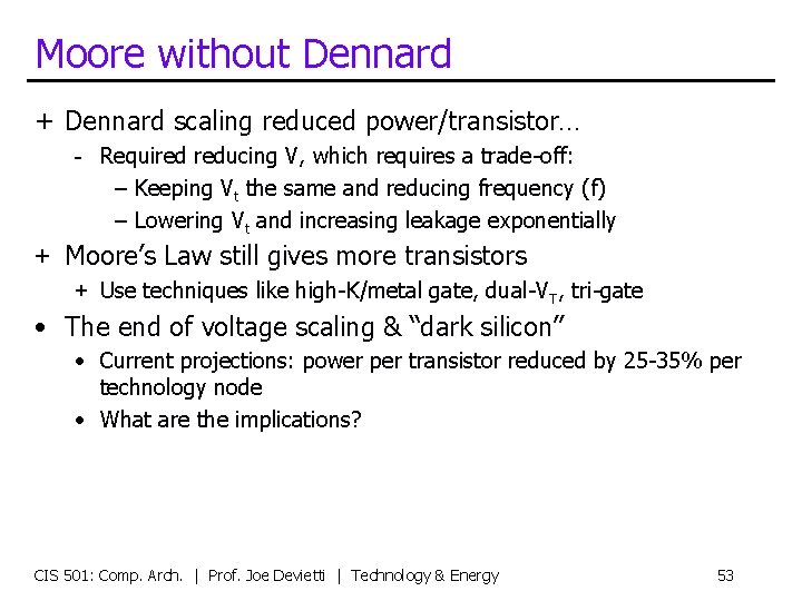
Moore without Dennard + Dennard scaling reduced power/transistor… - Required reducing V, which requires a trade-off: – Keeping Vt the same and reducing frequency (f) – Lowering Vt and increasing leakage exponentially + Moore’s Law still gives more transistors + Use techniques like high-K/metal gate, dual-VT, tri-gate • The end of voltage scaling & “dark silicon” • Current projections: power per transistor reduced by 25 -35% per technology node • What are the implications? CIS 501: Comp. Arch. | Prof. Joe Devietti | Technology & Energy 53

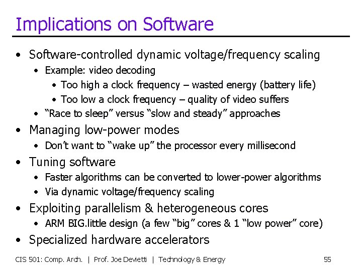
Implications on Software • Software-controlled dynamic voltage/frequency scaling • Example: video decoding • Too high a clock frequency – wasted energy (battery life) • Too low a clock frequency – quality of video suffers • “Race to sleep” versus “slow and steady” approaches • Managing low-power modes • Don’t want to “wake up” the processor every millisecond • Tuning software • Faster algorithms can be converted to lower-power algorithms • Via dynamic voltage/frequency scaling • Exploiting parallelism & heterogeneous cores • ARM BIG. little design (a few “big” cores & 1 “low power” core) • Specialized hardware accelerators CIS 501: Comp. Arch. | Prof. Joe Devietti | Technology & Energy 55

Summary CIS 501: Comp. Arch. | Prof. Joe Devietti | Technology & Energy 56

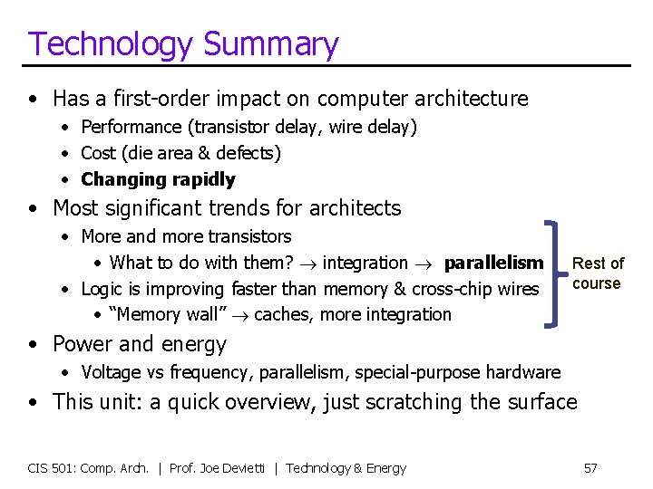
Technology Summary • Has a first-order impact on computer architecture • Performance (transistor delay, wire delay) • Cost (die area & defects) • Changing rapidly • Most significant trends for architects • More and more transistors • What to do with them? integration parallelism • Logic is improving faster than memory & cross-chip wires • “Memory wall” caches, more integration Rest of course • Power and energy • Voltage vs frequency, parallelism, special-purpose hardware • This unit: a quick overview, just scratching the surface CIS 501: Comp. Arch. | Prof. Joe Devietti | Technology & Energy 57