Chapter 5 Imperfections Interfacial and Volumetric Defects Grains
![Tilt Boundary Image and atomic position model of an approximately 32◦ [110] tilt boundary Tilt Boundary Image and atomic position model of an approximately 32◦ [110] tilt boundary](https://slidetodoc.com/presentation_image/3d7ef434db3a69398fe6d67d19593837/image-15.jpg)
- Slides: 37

Chapter 5 Imperfections: Interfacial and Volumetric Defects

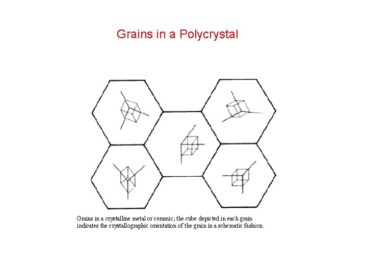
Grains in a Polycrystal Grains in a crystalline metal or ceramic; the cube depicted in each grain indicates the crystallographic orientation of the grain in a schematic fashion.

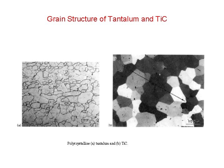
Grain Structure of Tantalum and Ti. C Polycrystalline (a) tantalum and (b) Ti. C.

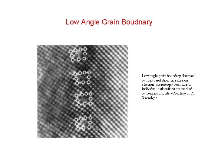
Low Angle Grain Boudnary Low-angle grain boundary observed by high-resolution transmission electron microscopy. Positions of individual dislocations are marked by Burgers circuits. (Courtesy of R. Gronsky. )

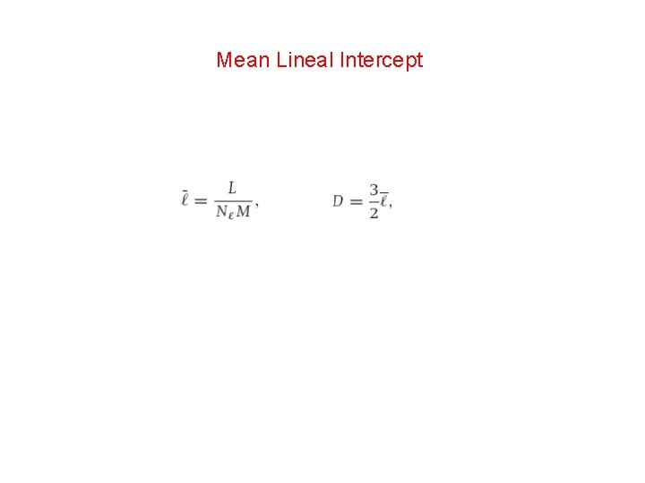
Mean Lineal Intercept

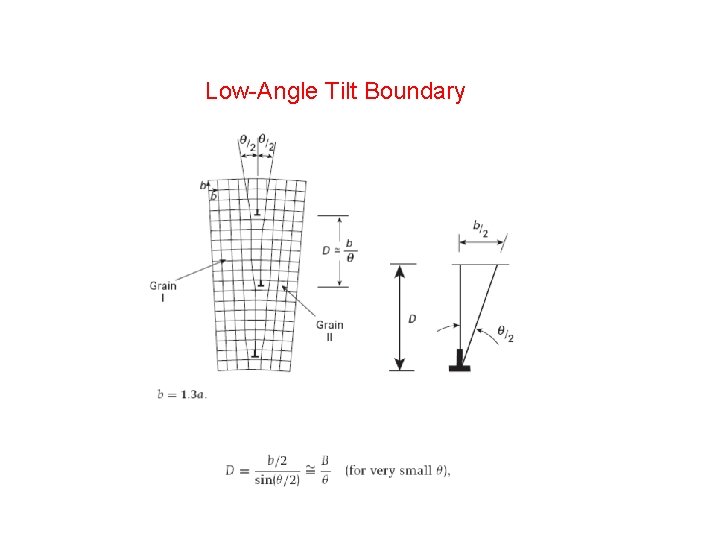
Low-Angle Tilt Boundary

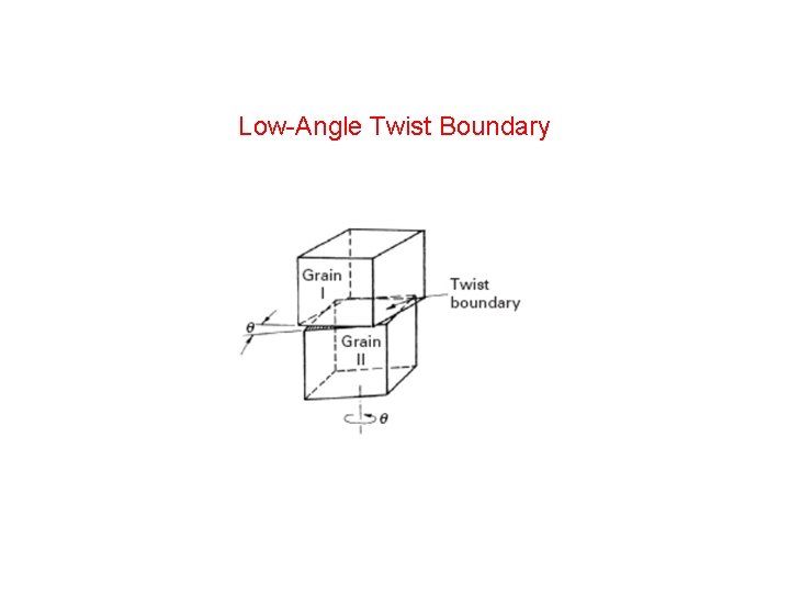
Low-Angle Twist Boundary

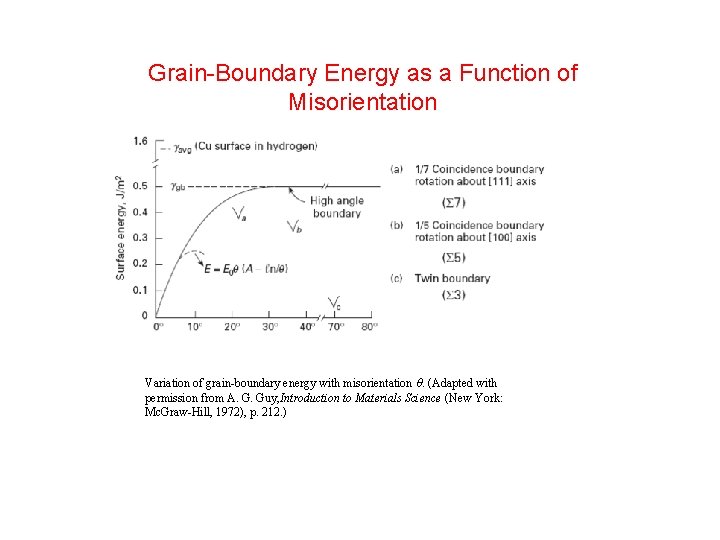
Grain-Boundary Energy as a Function of Misorientation Variation of grain-boundary energy with misorientation θ. (Adapted with permission from A. G. Guy, Introduction to Materials Science (New York: Mc. Graw-Hill, 1972), p. 212. )

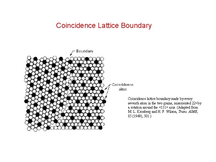
Coincidence Lattice Boundary Coincidence lattice boundary made by every seventh atom in the two grains, misoriented 22◦ by a rotation around the <111> axis. (Adapted from M. L. Kronberg and H. F. Wilson, Trans. AIME, 85 (1949), 501. )

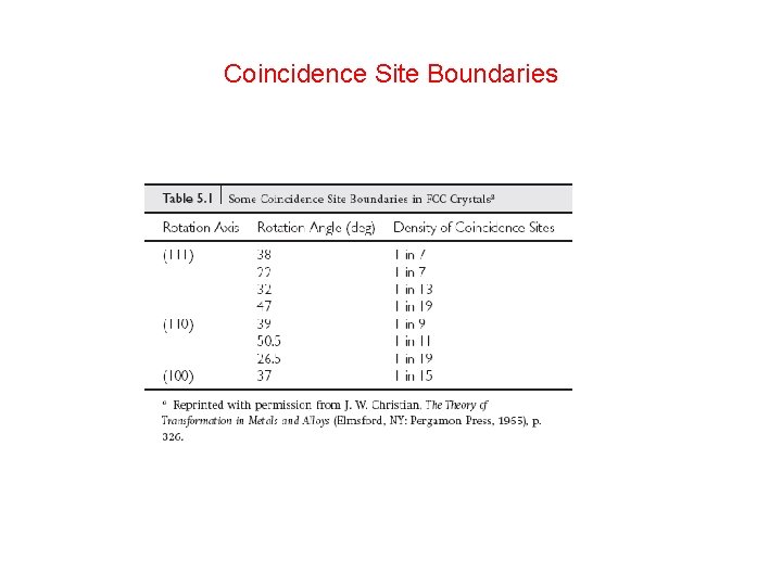
Coincidence Site Boundaries

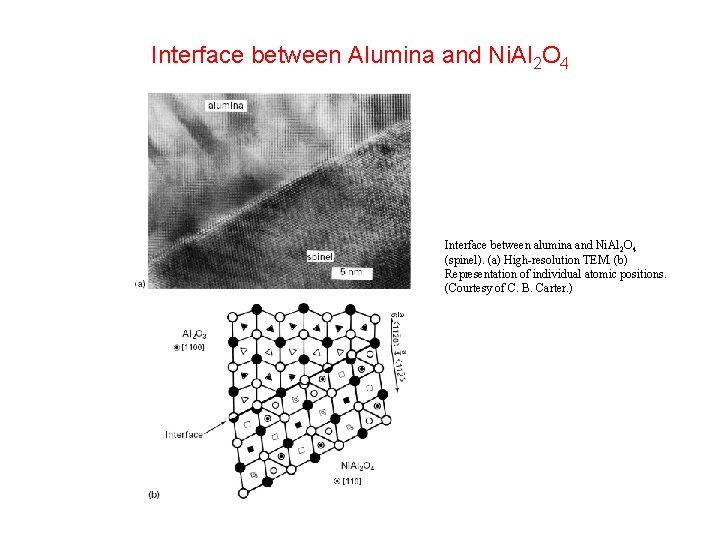
Interface between Alumina and Ni. Al 2 O 4 Interface between alumina and Ni. Al 2 O 4 (spinel). (a) High-resolution TEM. (b) Representation of individual atomic positions. (Courtesy of C. B. Carter. )

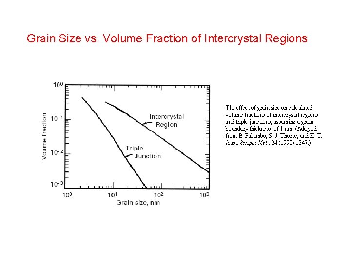
Grain Size vs. Volume Fraction of Intercrystal Regions The effect of grain size on calculated volume fractions of intercrystal regions and triple junctions, assuming a grain boundary thickness of 1 nm. (Adapted from B. Palumbo, S. J. Thorpe, and K. T. Aust, Scripta Met. , 24 (1990) 1347. )

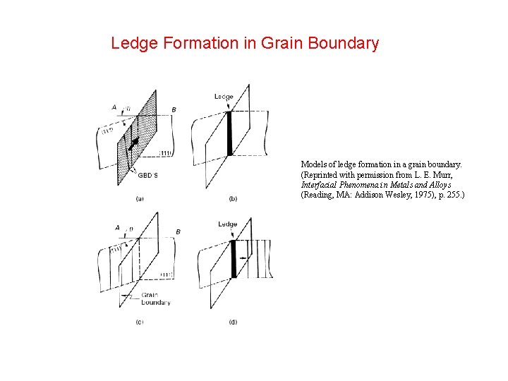
Ledge Formation in Grain Boundary Models of ledge formation in a grain boundary. (Reprinted with permission from L. E. Murr, Interfacial Phenomena in Metals and Alloys (Reading, MA: Addison Wesley, 1975), p. 255. )

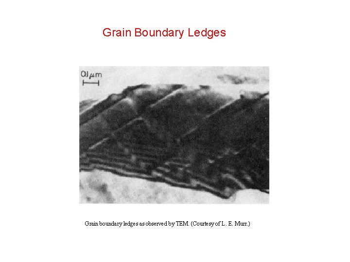
Grain Boundary Ledges Grain boundary ledges as observed by TEM. (Courtesy of L. E. Murr. )
![Tilt Boundary Image and atomic position model of an approximately 32 110 tilt boundary Tilt Boundary Image and atomic position model of an approximately 32◦ [110] tilt boundary](https://slidetodoc.com/presentation_image/3d7ef434db3a69398fe6d67d19593837/image-15.jpg)
Tilt Boundary Image and atomic position model of an approximately 32◦ [110] tilt boundary in gold; note the arrangement of polygons representing the boundary. (From W. Krakow and D. A. Smith, J. Mater. Res. 22 (1986) 54. )

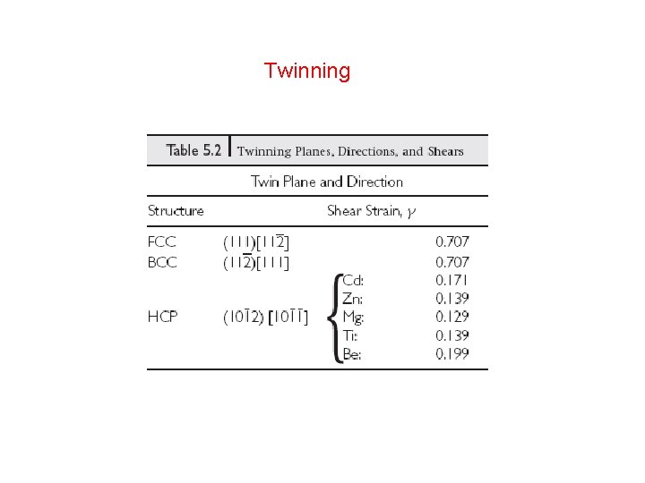
Twinning

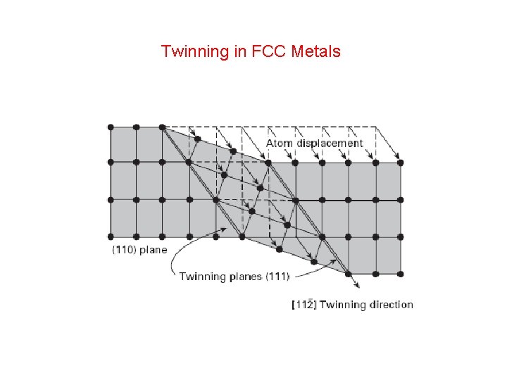
Twinning in FCC Metals

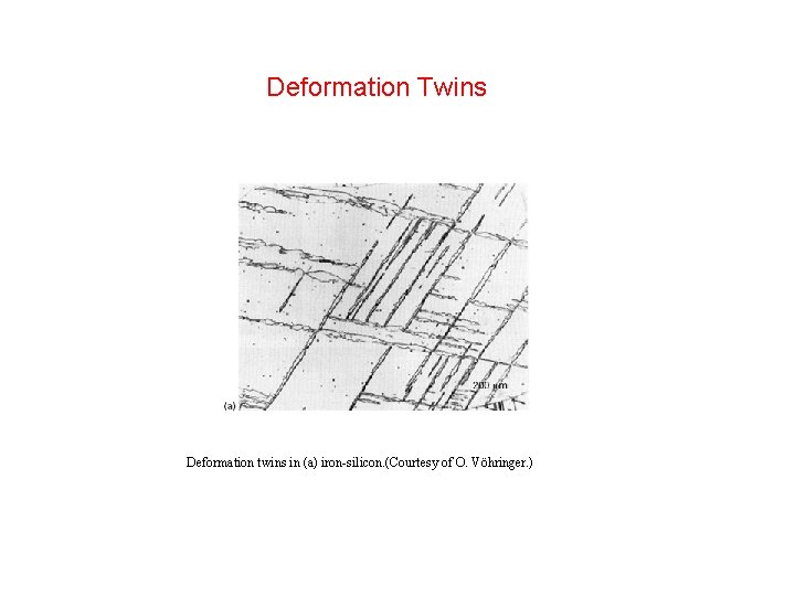
Deformation Twins Deformation twins in (a) iron-silicon. (Courtesy of O. Vöhringer. )

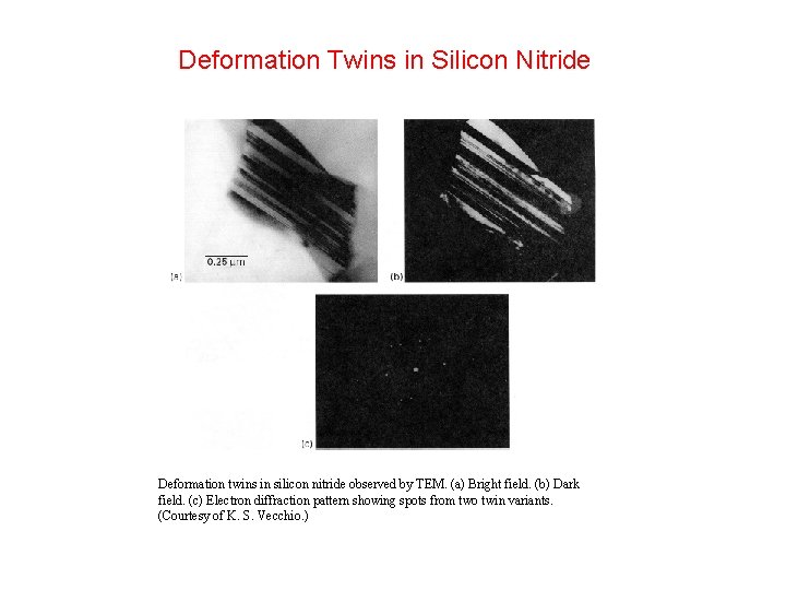
Deformation Twins in Silicon Nitride Deformation twins in silicon nitride observed by TEM. (a) Bright field. (b) Dark field. (c) Electron diffraction pattern showing spots from two twin variants. (Courtesy of K. S. Vecchio. )

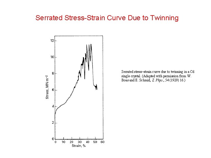
Serrated Stress-Strain Curve Due to Twinning Serrated stress–strain curve due to twinning in a Cd single crystal. (Adapted with permission from W. Boas and E. Schmid, Z. Phys. , 54 (1929) 16. )

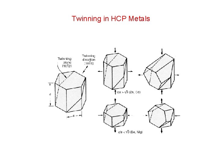
Twinning in HCP Metals

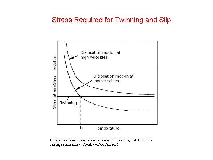
Stress Required for Twinning and Slip Effect of temperature on the stress required for twinning and slip (at low and high strain rates). (Courtesy of G. Thomas. )

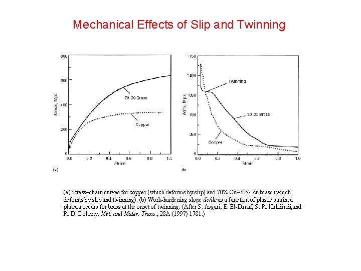
Mechanical Effects of Slip and Twinning (a) Stress–strain curves for copper (which deforms by slip) and 70% Cu– 30% Zn brass (which deforms by slip and twinning). (b) Work-hardening slope dσ/dε as a function of plastic strain; a plateau occurs for brass at the onset of twinning. (After S. Asgari, E. El-Danaf, S. R. Kalidindi, and R. D. Doherty, Met. and Mater. Trans. , 28 A (1997) 1781. )

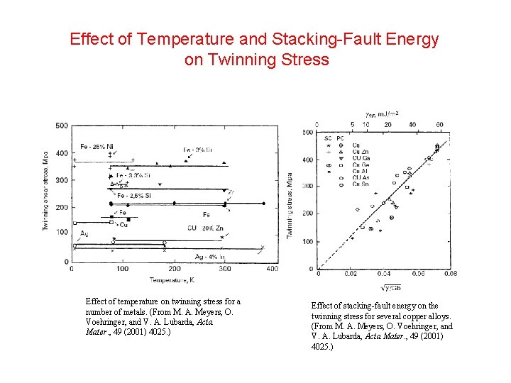
Effect of Temperature and Stacking-Fault Energy on Twinning Stress Effect of temperature on twinning stress for a number of metals. (From M. A. Meyers, O. Voehringer, and V. A. Lubarda, Acta Mater. , 49 (2001) 4025. ) Effect of stacking-fault energy on the twinning stress for several copper alloys. (From M. A. Meyers, O. Voehringer, and V. A. Lubarda, Acta Mater. , 49 (2001) 4025. )

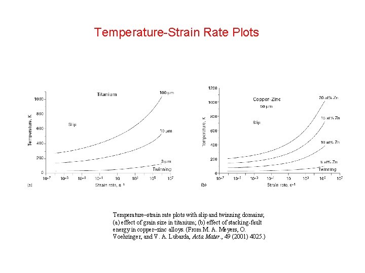
Temperature-Strain Rate Plots Temperature–strain rate plots with slip and twinning domains; (a) effect of grain size in titanium; (b) effect of stacking-fault energy in copper–zinc alloys. (From M. A. Meyers, O. Voehringer, and V. A. Lubarda, Acta Mater. , 49 (2001) 4025. )

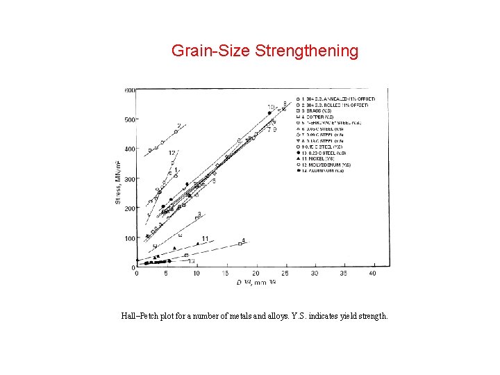
Grain-Size Strengthening Hall–Petch plot for a number of metals and alloys. Y. S. indicates yield strength.

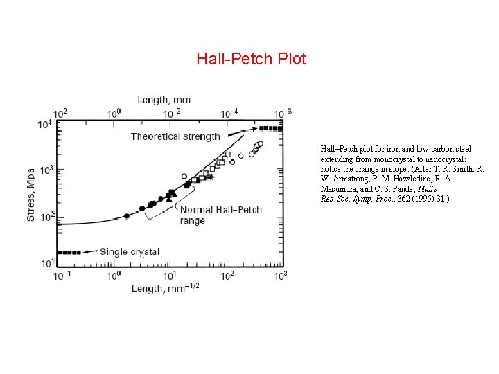
Hall-Petch Plot Hall–Petch plot for iron and low-carbon steel extending from monocrystal to nanocrystal; notice the change in slope. (After T. R. Smith, R. W. Armstrong, P. M. Hazzledine, R. A. Masumura, and C. S. Pande, Matls. Res. Soc. Symp. Proc. , 362 (1995) 31. )

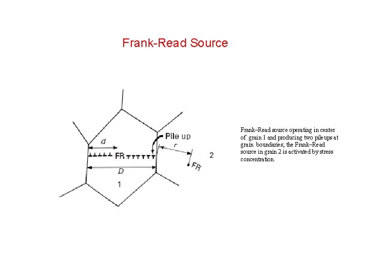
Frank-Read Source Frank–Read source operating in center of grain 1 and producing two pileups at grain boundaries; the Frank–Read source in grain 2 is activated by stress concentration.

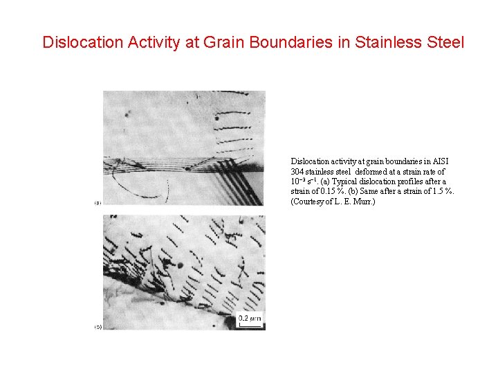
Dislocation Activity at Grain Boundaries in Stainless Steel Dislocation activity at grain boundaries in AISI 304 stainless steel deformed at a strain rate of 10− 3 s− 1. (a) Typical dislocation profiles after a strain of 0. 15 %. (b) Same after a strain of 1. 5 %. (Courtesy of L. E. Murr. )

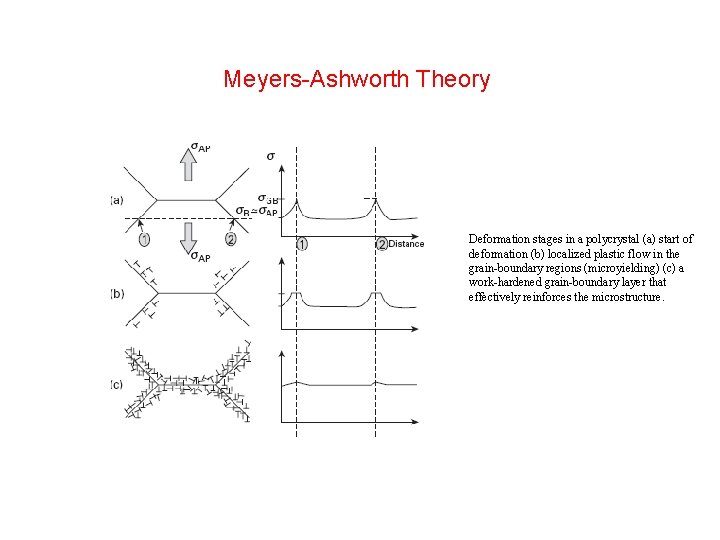
Meyers-Ashworth Theory Deformation stages in a polycrystal (a) start of deformation (b) localized plastic flow in the grain-boundary regions (microyielding) (c) a work-hardened grain-boundary layer that effectively reinforces the microstructure.

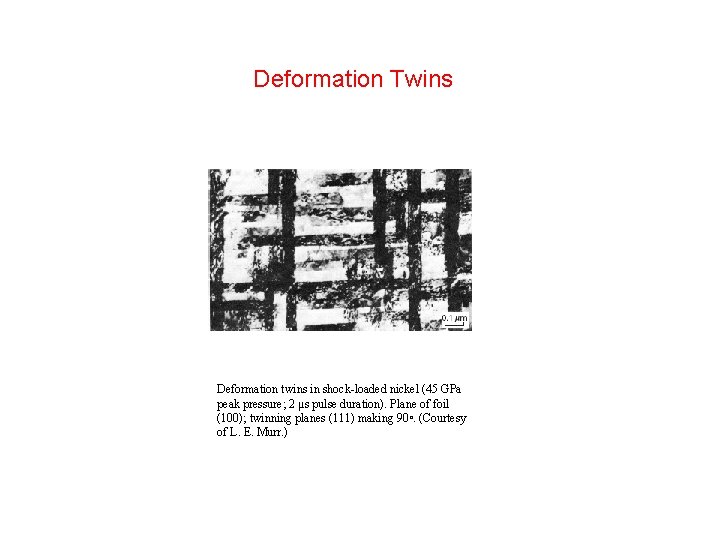
Deformation Twins Deformation twins in shock-loaded nickel (45 GPa peak pressure; 2 μs pulse duration). Plane of foil (100); twinning planes (111) making 90◦. (Courtesy of L. E. Murr. )

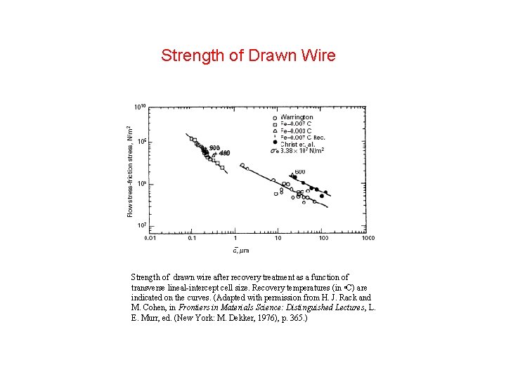
Strength of Drawn Wire Strength of drawn wire after recovery treatment as a function of transverse lineal-intercept cell size. Recovery temperatures (in ◦C) are indicated on the curves. (Adapted with permission from H. J. Rack and M. Cohen, in Frontiers in Materials Science: Distinguished Lectures, L. E. Murr, ed. (New York: M. Dekker, 1976), p. 365. )

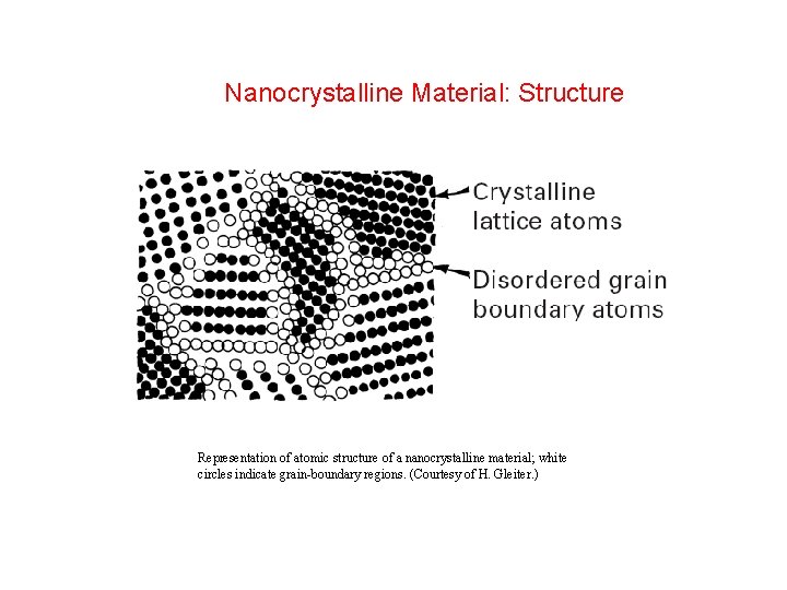
Nanocrystalline Material: Structure Representation of atomic structure of a nanocrystalline material; white circles indicate grain-boundary regions. (Courtesy of H. Gleiter. )

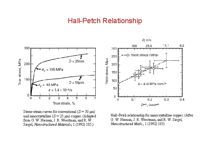
Hall-Petch Relationship Stress–strain curves for conventional (D = 50 μm) and nanocrystalline (D = 25 μm) copper. (Adapted from G. W. Nieman, J. R. Weertman, and R. W. Siegel, Nanostructured Materials, 1 (1992) 185. ) Hall–Petch relationship for nanocrystalline copper. (After G. W. Nieman, J. R. Weertman, and R. W. Siegel, Nanostructured Matls. , 1 (1992) 185)

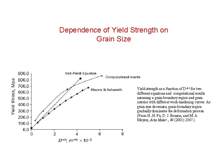
Dependence of Yield Strength on Grain Size Yield strength as a function of D − 0. 5 for two different equations and computational results assuming a grain-boundary region and grain interior with different work-hardening curves. As grain size decreases, grain-boundary region gradually dominates the deformation process. (From H. -H. Fu, D. J. Benson, and M. A. Meyers, Acta Mater. , 49 (2001) 2567. )

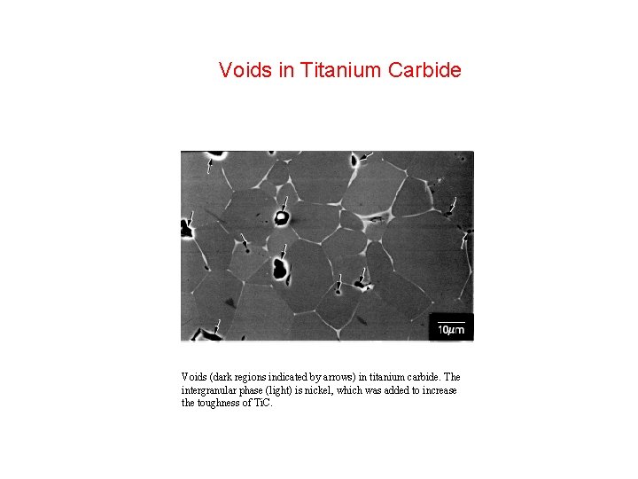
Voids in Titanium Carbide Voids (dark regions indicated by arrows) in titanium carbide. The intergranular phase (light) is nickel, which was added to increase the toughness of Ti. C.

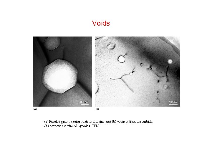
Voids (a) Faceted grain-interior voids in alumina and (b) voids in titanium carbide; dislocations are pinned by voids. TEM.