ANALOG CIRCUITS 16 MARKS OPERATIONAL AMPLIFIEROPAMP OpAmp An


- Slides: 28
ANALOG CIRCUITS 16 MARKS
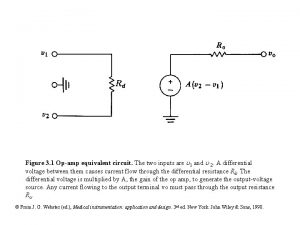
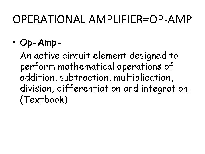
OPERATIONAL AMPLIFIER=OP-AMP • Op-Amp. An active circuit element designed to perform mathematical operations of addition, subtraction, multiplication, division, differentiation and integration. (Textbook)
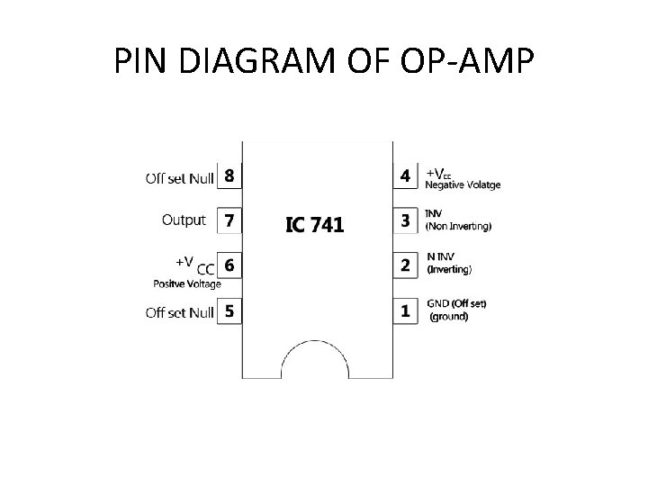
PIN DIAGRAM OF OP-AMP
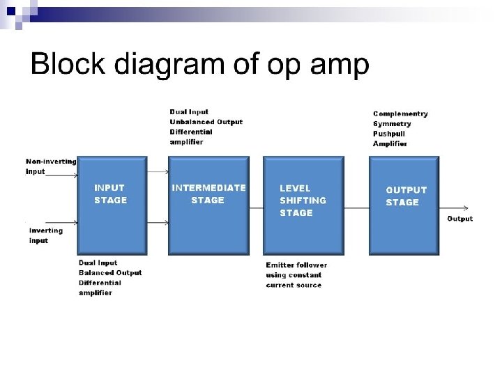
BLOCK DIAGRAM OF OP-AMP
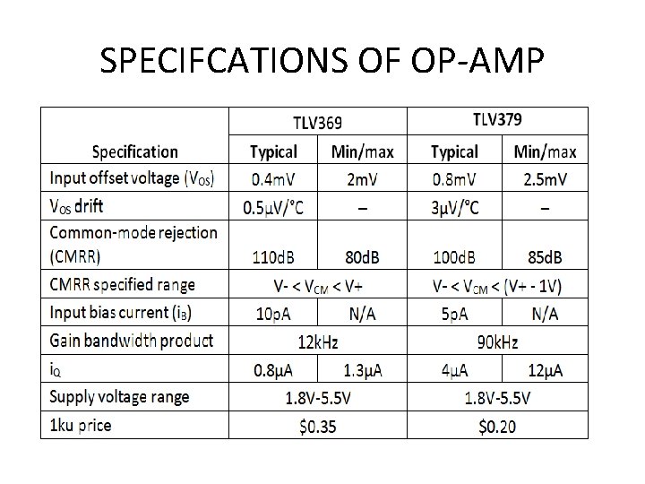
SPECIFCATIONS OF OP-AMP
APPLICATIONS OF OP-AMP
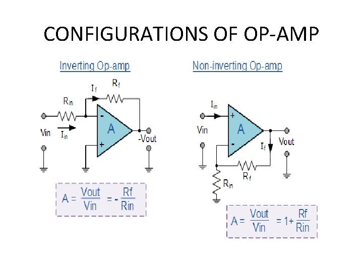
CONFIGURATIONS OF OP-AMP
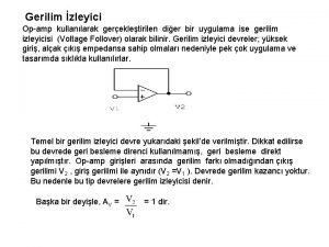
Inverting & Non-inverting amplifier • The negative sign in the equation indicates an inversion of the output signal with respect to the input as it is 180 o out of phase. • useful application of an inverting amplifier is that of a “transresistance amplifier” • The positie sign in the equation indicates an inversion of the output signal with respect to the input as it is inphase.
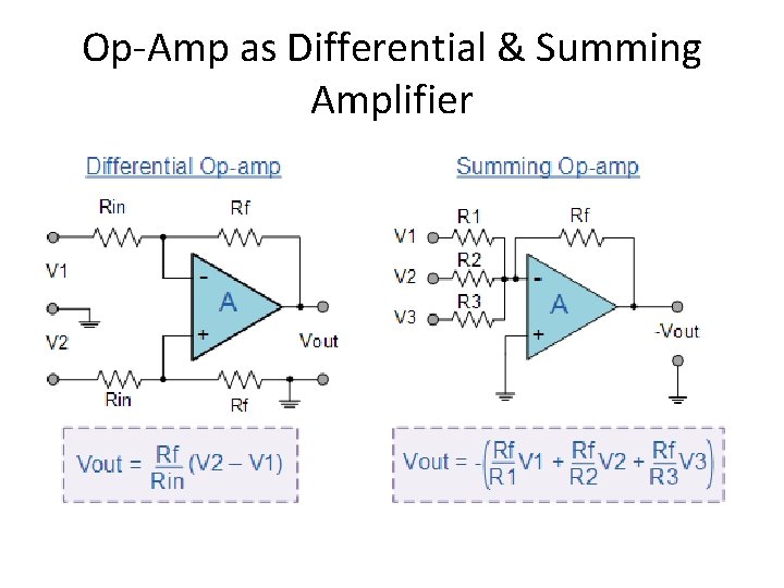
Op-Amp as Differential & Summing Amplifier
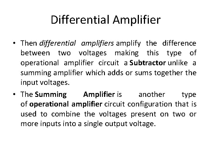
Differential Amplifier • Then differential amplifiers amplify the difference between two voltages making this type of operational amplifier circuit a Subtractor unlike a summing amplifier which adds or sums together the input voltages. • The Summing Amplifier is another type of operational amplifier circuit configuration that is used to combine the voltages present on two or more inputs into a single output voltage.
Instrumentation Amplifier
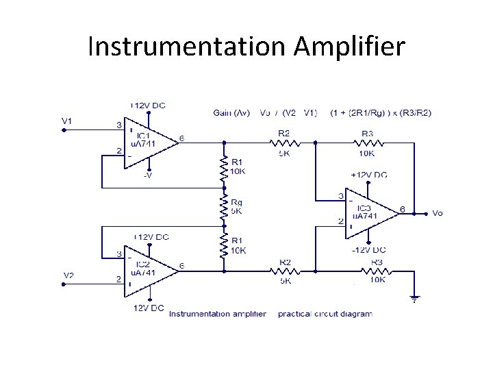
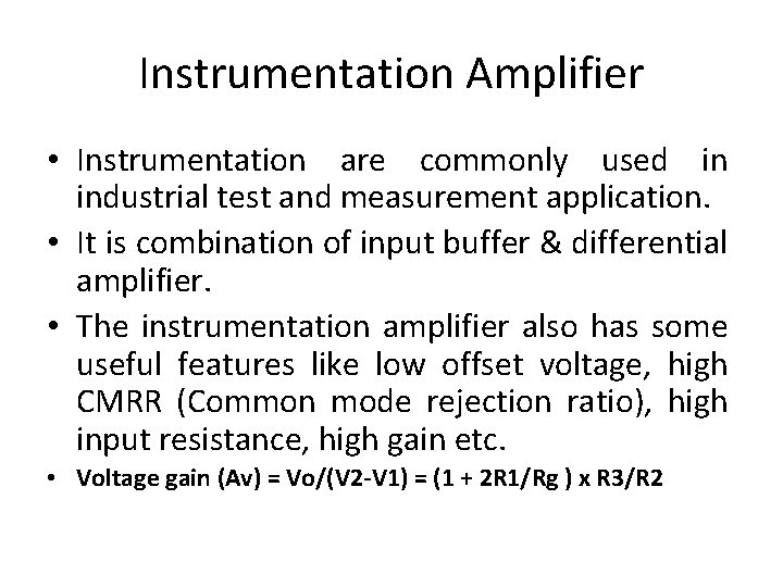
Instrumentation Amplifier • Instrumentation are commonly used in industrial test and measurement application. • It is combination of input buffer & differential amplifier. • The instrumentation amplifier also has some useful features like low offset voltage, high CMRR (Common mode rejection ratio), high input resistance, high gain etc. • Voltage gain (Av) = Vo/(V 2 -V 1) = (1 + 2 R 1/Rg ) x R 3/R 2
Integrator & Differentiator
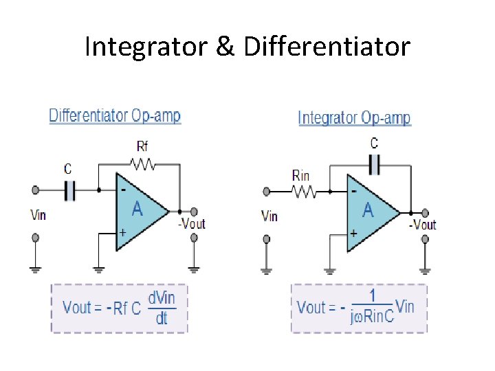
Integrator • Op-amp Integrator is an operational amplifier circuit that performs the mathematical operation of Integration. • can cause the output to respond to changes in the input voltage over time as the op-amp integrator produces an output voltage which is proportional to the integral of the input voltage.
Differentiator • This operational amplifier circuit performs the mathematical operation of Differentiation. • that is it “produces a voltage output which is directly proportional to the input voltage’s rate-of-change with respect to time“.
IC 555 – TIMER • The 555 timer IC is an integrated circuit(chip) used in a variety of timer, pulse generation, and oscillator applications. • The 555 can be used to provide time delays, as an oscillator, and as a flip-flop element.
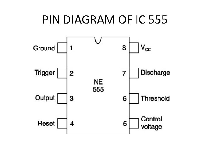
PIN DIAGRAM OF IC 555
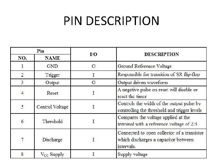
PIN DESCRIPTION
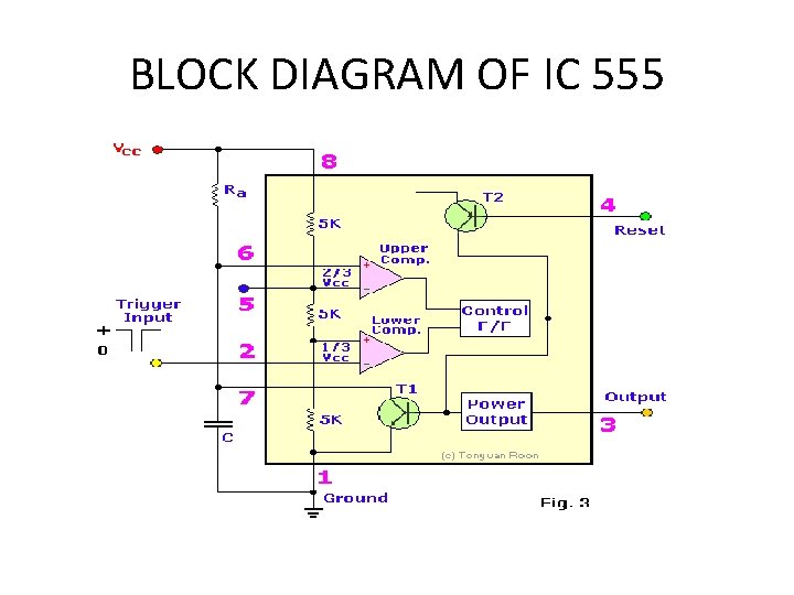
BLOCK DIAGRAM OF IC 555
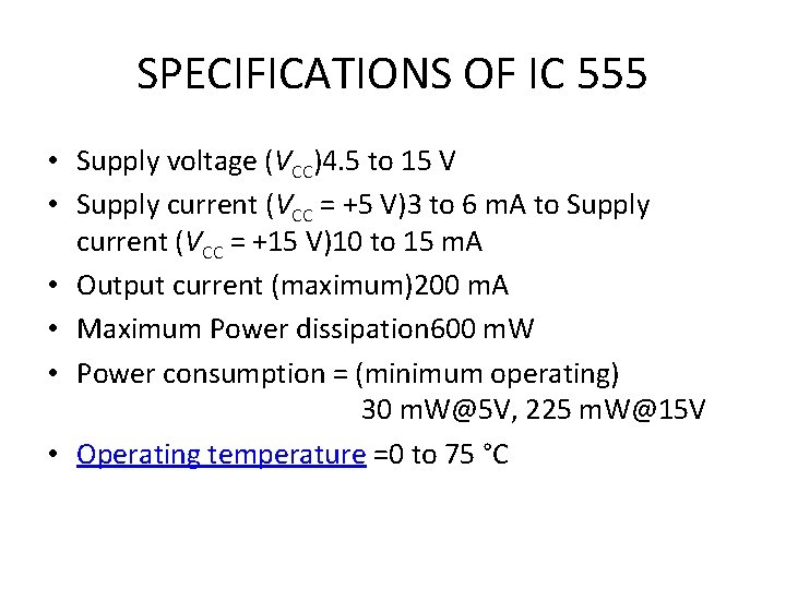
SPECIFICATIONS OF IC 555 • Supply voltage (VCC)4. 5 to 15 V • Supply current (VCC = +5 V)3 to 6 m. A to Supply current (VCC = +15 V)10 to 15 m. A • Output current (maximum)200 m. A • Maximum Power dissipation 600 m. W • Power consumption = (minimum operating) 30 m. W@5 V, 225 m. W@15 V • Operating temperature =0 to 75 °C
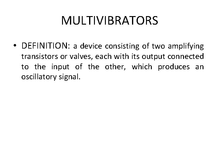
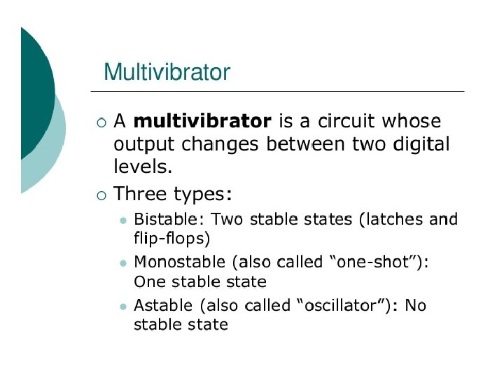
MULTIVIBRATORS • DEFINITION: a device consisting of two amplifying transistors or valves, each with its output connected to the input of the other, which produces an oscillatory signal.
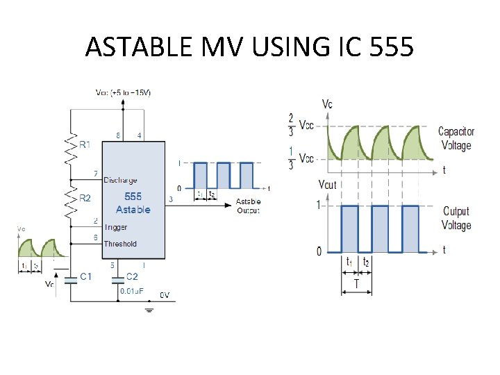
ASTABLE MV USING IC 555
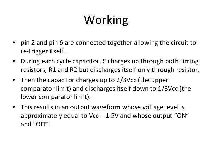
Working • pin 2 and pin 6 are connected together allowing the circuit to re-trigger itself. • During each cycle capacitor, C charges up through both timing resistors, R 1 and R 2 but discharges itself only through resistor. • Then the capacitor charges up to 2/3 Vcc (the upper comparator limit) and discharges itself down to 1/3 Vcc (the lower comparator limit). • This results in an output waveform whose voltage level is approximately equal to Vcc – 1. 5 V and whose output “ON” and “OFF”.
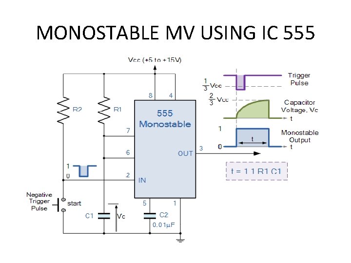
MONOSTABLE MV USING IC 555
WORKING • When a negative ( 0 V ) pulse is applied to the trigger input (pin 2). • the internal comparator, (comparator No 1) detects this input and “sets” the state of the flip-flop from low to high. • This turn off discharge transistor connected to pin 7. • This action allows the timing capacitor to start to charge up through resistor, R 1 until the voltage across the capacitor reaches the threshold (pin 6) voltage of 2/3 Vcc. • At this point the comparators output goes “HIGH” and “resets” the flip-flop back to its original state which in turns “ON” the transistor and discharges the capacitor to ground through pin 7. • This causes the output to change its state back to the original stable “LOW” value awaiting another trigger pulse to start the timing process over again.
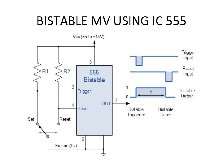
BISTABLE MV USING IC 555
WORKING • The switching of the output waveform is achieved by controlling the trigger and reset inputs of the 555 timer which are held “HIGH” by the two pull-up resistors, R 1 and R 2. • By taking the trigger input (pin 2) “LOW”, switch in set position, changes the output state into the “HIGH” state and by taking the reset input (pin 4) “LOW”, switch in reset position, changes the output into the “LOW” state. • Then the Bistable 555 timer is stable in both states, “HIGH” and “LOW”. The threshold input (pin 6) is connected to ground to ensure that it cannot reset the bistable circuit as it would in a normal timing application.