Analog and RF Circuit Testing Suraj Sindia Vishwani
- Slides: 38

Analog and RF Circuit Testing Suraj Sindia Vishwani D. Agrawal Auburn University ECE Dept. , Auburn, AL 36849, USA www. eng. auburn. edu/~vagrawal Education Day, VDAT, July 2, 2012 Education Day: Sindia and Agrawal 1

Outline • Introduction to analog/RF circuit test • Techniques for analog/RF circuit test – Specification based test with examples – Alternate test with examples • Conclusion July 2, 2012 Education Day: Sindia and Agrawal 2

Outline • Introduction to analog/RF circuit test • Techniques for analog/RF circuit test – Specification based test with examples – Alternate test with examples • Conclusion July 2, 2012 Education Day: Sindia and Agrawal 3

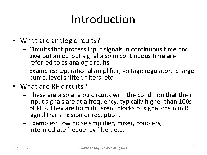
Introduction • What are analog circuits? – Circuits that process input signals in continuous time and give out an output signal also in continuous time are referred to as analog circuits. – Examples: Operational amplifier, voltage regulator, charge pump, level shifter, filters, etc. • What are RF circuits? – These are also analog circuits with the condition that their input signals are at a frequency, typically higher than 100 s of k. Hz. They are form different blocks of signal chain in RF signal transmission or reception. – Examples: Low noise amplifier, mixer, couplers, intermediate frequency filter, etc. July 2, 2012 Education Day: Sindia and Agrawal 4

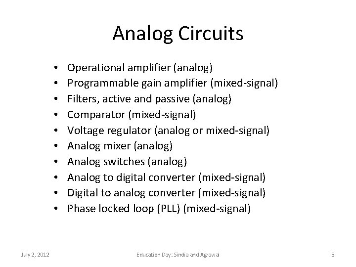
Analog Circuits • • • July 2, 2012 Operational amplifier (analog) Programmable gain amplifier (mixed-signal) Filters, active and passive (analog) Comparator (mixed-signal) Voltage regulator (analog or mixed-signal) Analog mixer (analog) Analog switches (analog) Analog to digital converter (mixed-signal) Digital to analog converter (mixed-signal) Phase locked loop (PLL) (mixed-signal) Education Day: Sindia and Agrawal 5

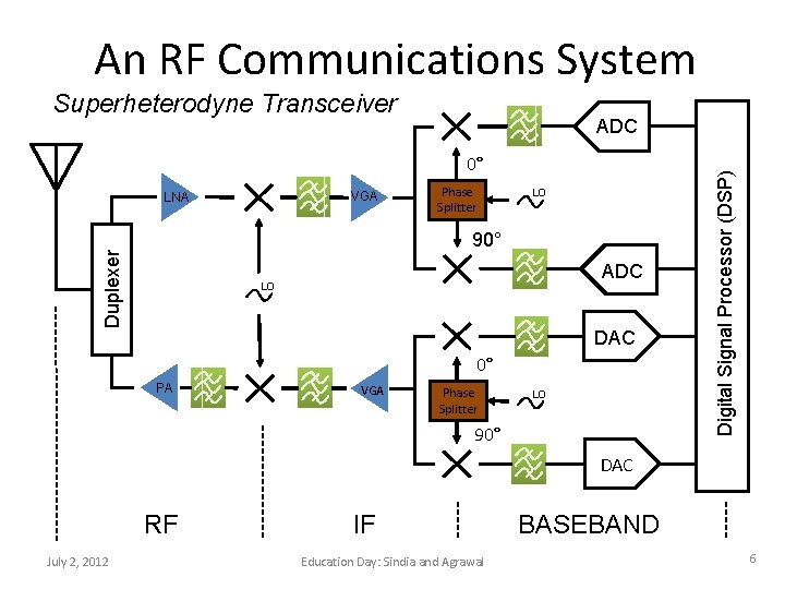
An RF Communications System Superheterodyne Transceiver 0° VGA LNA Phase Splitter LO Duplexer 90° ADC LO DAC 0° PA VGA Phase Splitter LO 90° Digital Signal Processor (DSP) ADC DAC RF July 2, 2012 IF Education Day: Sindia and Agrawal BASEBAND 6

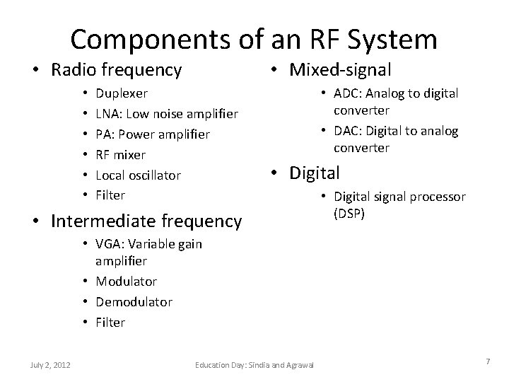
Components of an RF System • Radio frequency • • Mixed-signal Duplexer LNA: Low noise amplifier PA: Power amplifier RF mixer Local oscillator Filter • ADC: Analog to digital converter • DAC: Digital to analog converter • Digital • Intermediate frequency • Digital signal processor (DSP) • VGA: Variable gain amplifier • Modulator • Demodulator • Filter July 2, 2012 Education Day: Sindia and Agrawal 7

Why Do We Test Analog/RF Circuits? • Follows from the philosophy of testing: – Manufacturing defects and process variation cause a circuit to deviate from its intended behavior. – Testing circuits, ensures that they meet their desired behavior within the limits specified by the system. July 2, 2012 Education Day: Sindia and Agrawal 8

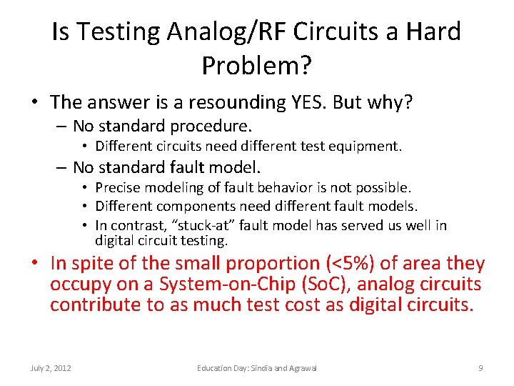
Is Testing Analog/RF Circuits a Hard Problem? • The answer is a resounding YES. But why? – No standard procedure. • Different circuits need different test equipment. – No standard fault model. • Precise modeling of fault behavior is not possible. • Different components need different fault models. • In contrast, “stuck-at” fault model has served us well in digital circuit testing. • In spite of the small proportion (<5%) of area they occupy on a System-on-Chip (So. C), analog circuits contribute to as much test cost as digital circuits. July 2, 2012 Education Day: Sindia and Agrawal 9

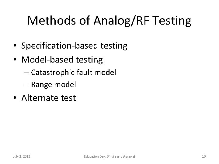
Methods of Analog/RF Testing • Specification-based testing • Model-based testing – Catastrophic fault model – Range model • Alternate test July 2, 2012 Education Day: Sindia and Agrawal 10

Outline • Introduction to analog/RF circuit test • Techniques for analog/RF circuit test – Specification based test with examples – Alternate test with examples • Conclusion July 2, 2012 Education Day: Sindia and Agrawal 11

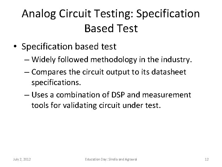
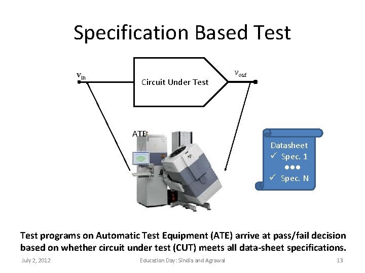
Analog Circuit Testing: Specification Based Test • Specification based test – Widely followed methodology in the industry. – Compares the circuit output to its datasheet specifications. – Uses a combination of DSP and measurement tools for validating circuit under test. July 2, 2012 Education Day: Sindia and Agrawal 12

Specification Based Test vin Circuit Under Test vout ATE Datasheet ü Spec. 1 ●●● ü Spec. N Test programs on Automatic Test Equipment (ATE) arrive at pass/fail decision based on whether circuit under test (CUT) meets all data-sheet specifications. July 2, 2012 Education Day: Sindia and Agrawal 13

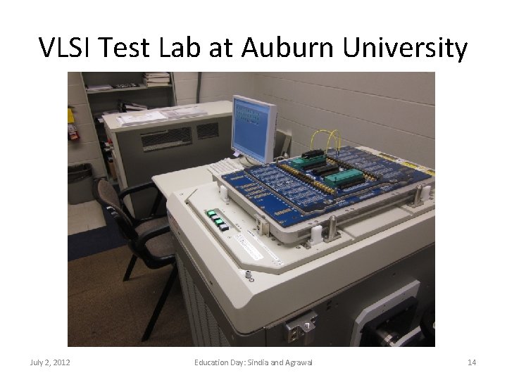
VLSI Test Lab at Auburn University July 2, 2012 Education Day: Sindia and Agrawal 14

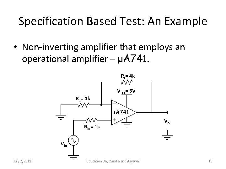
Specification Based Test: An Example • Non-inverting amplifier that employs an operational amplifier – μA 741. Rf= 4 k R 1= 1 k VDD= 5 V μA 741 Rin= 1 k Vo Vin July 2, 2012 Education Day: Sindia and Agrawal 15

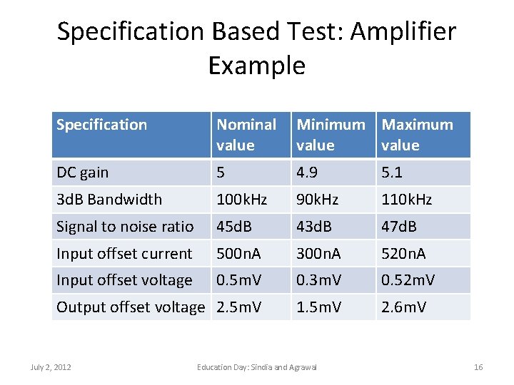
Specification Based Test: Amplifier Example Specification Nominal value Minimum Maximum value DC gain 5 4. 9 5. 1 3 d. B Bandwidth 100 k. Hz 90 k. Hz 110 k. Hz Signal to noise ratio 45 d. B 43 d. B 47 d. B Input offset current 500 n. A 300 n. A 520 n. A Input offset voltage 0. 5 m. V 0. 3 m. V 0. 52 m. V Output offset voltage 2. 5 m. V 1. 5 m. V 2. 6 m. V July 2, 2012 Education Day: Sindia and Agrawal 16

Specification Based Test: Procedure • Each specification is measured for circuit under test (CUT). • Measured value is verified to be within minimum/maximum limits. • CUT is labeled GOOD, if and only if all measured specifications are within limits, else it is rejected. July 2, 2012 Education Day: Sindia and Agrawal 17

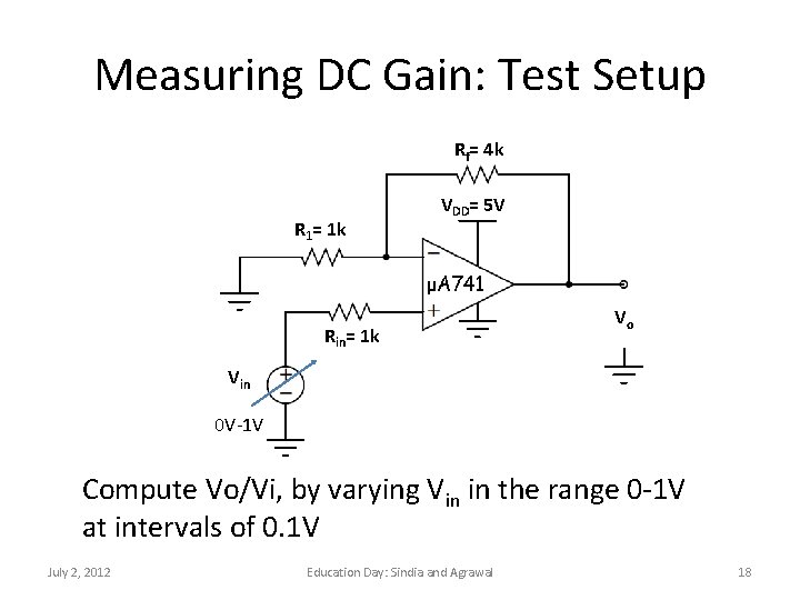
Measuring DC Gain: Test Setup Rf= 4 k R 1= 1 k VDD= 5 V μA 741 Rin= 1 k Vo Vin 0 V-1 V Compute Vo/Vi, by varying Vin in the range 0 -1 V at intervals of 0. 1 V July 2, 2012 Education Day: Sindia and Agrawal 18

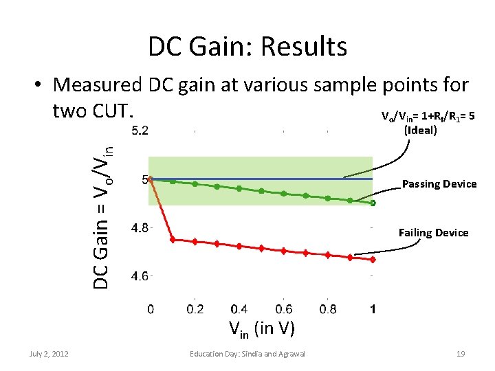
DC Gain: Results • Measured DC gain at various sample points for two CUT. V /V = 1+R /R = 5 DC Gain = Vo/Vin o in (Ideal) f 1 Passing Device Failing Device Vin (in V) July 2, 2012 Education Day: Sindia and Agrawal 19

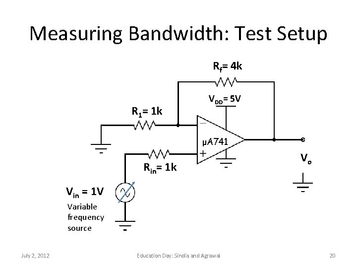
Measuring Bandwidth: Test Setup Rf= 4 k R 1= 1 k VDD= 5 V μA 741 Rin= 1 k Vo Vin = 1 V Variable frequency source July 2, 2012 Education Day: Sindia and Agrawal 20

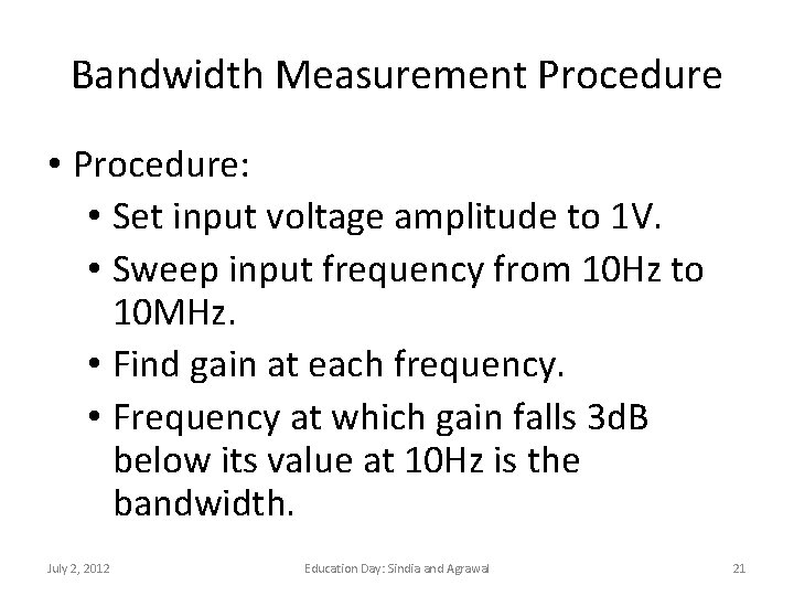
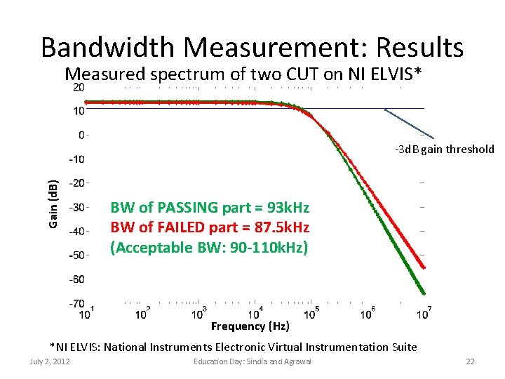
Bandwidth Measurement Procedure • Procedure: • Set input voltage amplitude to 1 V. • Sweep input frequency from 10 Hz to 10 MHz. • Find gain at each frequency. • Frequency at which gain falls 3 d. B below its value at 10 Hz is the bandwidth. July 2, 2012 Education Day: Sindia and Agrawal 21

Bandwidth Measurement: Results Measured spectrum of two CUT on NI ELVIS* Gain (d. B) -3 d. B gain threshold BW of PASSING part = 93 k. Hz BW of FAILED part = 87. 5 k. Hz (Acceptable BW: 90 -110 k. Hz) Frequency (Hz) *NI ELVIS: National Instruments Electronic Virtual Instrumentation Suite July 2, 2012 Education Day: Sindia and Agrawal 22

Outline • Introduction to analog/RF circuit test • Techniques for analog/RF circuit test – Specification based test with examples – Alternate test with examples • Conclusion July 2, 2012 Education Day: Sindia and Agrawal 23

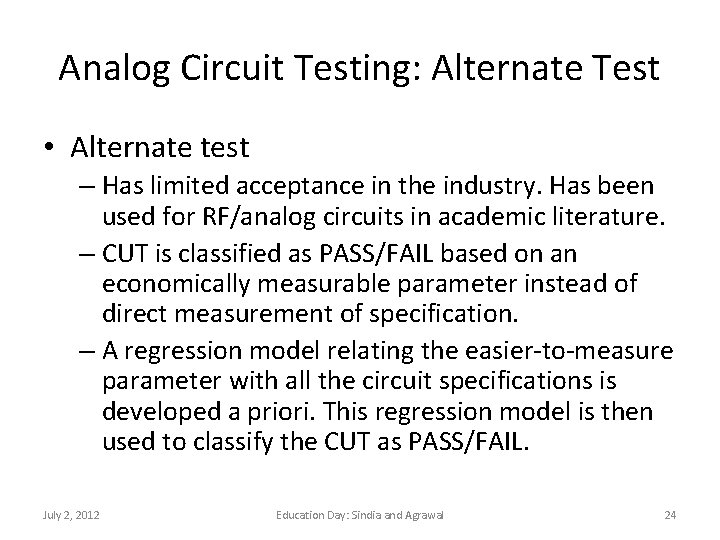
Analog Circuit Testing: Alternate Test • Alternate test – Has limited acceptance in the industry. Has been used for RF/analog circuits in academic literature. – CUT is classified as PASS/FAIL based on an economically measurable parameter instead of direct measurement of specification. – A regression model relating the easier-to-measure parameter with all the circuit specifications is developed a priori. This regression model is then used to classify the CUT as PASS/FAIL. July 2, 2012 Education Day: Sindia and Agrawal 24

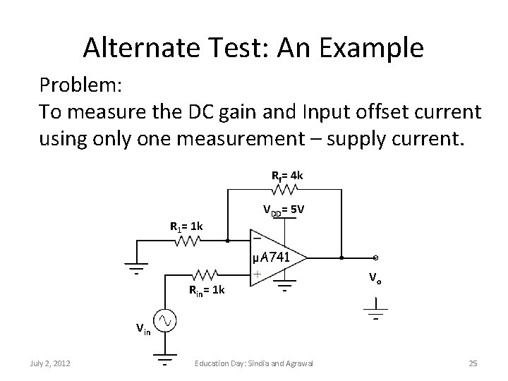
Alternate Test: An Example Problem: To measure the DC gain and Input offset current using only one measurement – supply current. Rf= 4 k R 1= 1 k VDD= 5 V μA 741 Rin= 1 k Vo Vin July 2, 2012 Education Day: Sindia and Agrawal 25

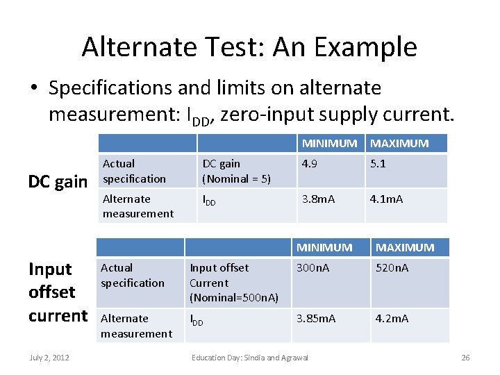
Alternate Test: An Example • Specifications and limits on alternate measurement: IDD, zero-input supply current. DC gain Input offset current July 2, 2012 MINIMUM MAXIMUM Actual specification DC gain (Nominal = 5) 4. 9 5. 1 Alternate measurement IDD 3. 8 m. A 4. 1 m. A MINIMUM MAXIMUM Actual specification Input offset Current (Nominal=500 n. A) 300 n. A 520 n. A Alternate measurement IDD 3. 85 m. A 4. 2 m. A Education Day: Sindia and Agrawal 26

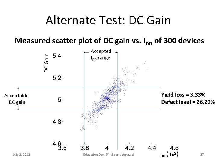
Alternate Test: DC Gain Measured scatter plot of DC gain vs. IDD of 300 devices Accepted IDD range Yield loss = 3. 33% Defect level = 26. 29% Acceptable DC gain July 2, 2012 Education Day: Sindia and Agrawal IDD (m. A) 27

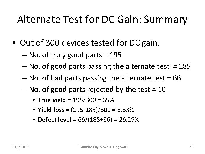
Alternate Test for DC Gain: Summary • Out of 300 devices tested for DC gain: – No. of truly good parts = 195 – No. of good parts passing the alternate test = 185 – No. of bad parts passing the alternate test = 66 – No. of good parts rejected by the test = 10 • True yield = 195/300 = 65% • Yield loss = (195 -185)/300 = 3. 33% • Defect level = 66/(185+66) = 26. 29% July 2, 2012 Education Day: Sindia and Agrawal 28

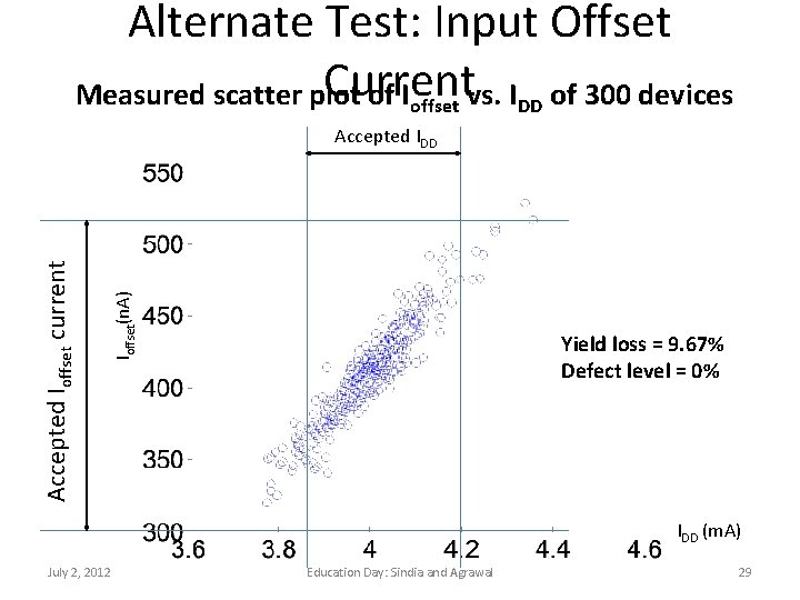
Alternate Test: Input Offset Current Measured scatter plot of Ioffset vs. IDD of 300 devices Ioffset(n. A) Accepted Ioffset current Accepted IDD Yield loss = 9. 67% Defect level = 0% IDD (m. A) July 2, 2012 Education Day: Sindia and Agrawal 29

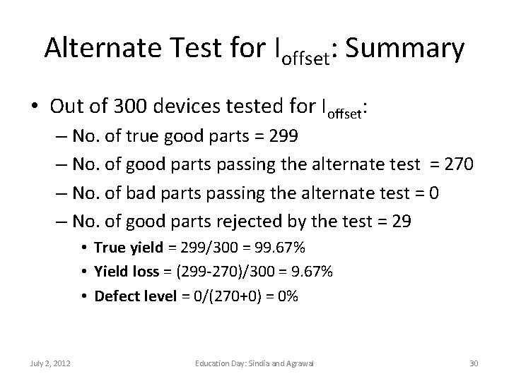
Alternate Test for Ioffset: Summary • Out of 300 devices tested for Ioffset: – No. of true good parts = 299 – No. of good parts passing the alternate test = 270 – No. of bad parts passing the alternate test = 0 – No. of good parts rejected by the test = 29 • True yield = 299/300 = 99. 67% • Yield loss = (299 -270)/300 = 9. 67% • Defect level = 0/(270+0) = 0% July 2, 2012 Education Day: Sindia and Agrawal 30

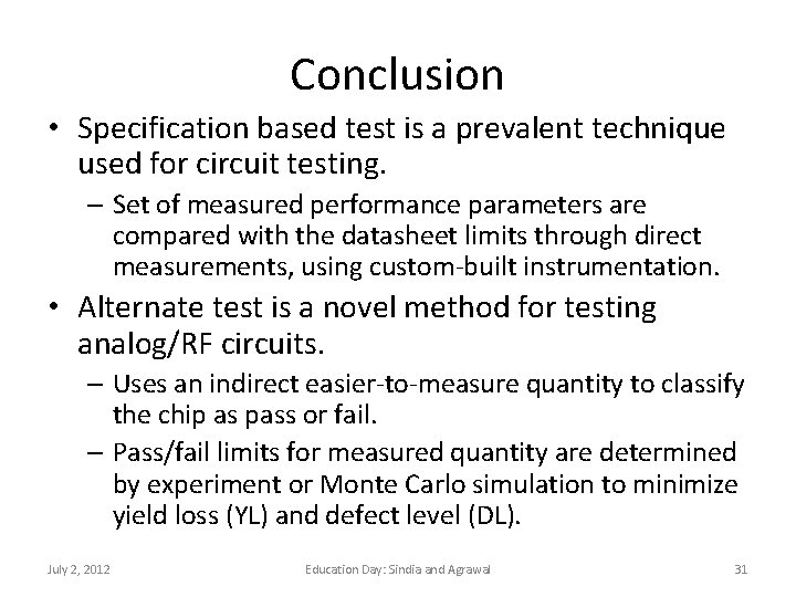
Conclusion • Specification based test is a prevalent technique used for circuit testing. – Set of measured performance parameters are compared with the datasheet limits through direct measurements, using custom-built instrumentation. • Alternate test is a novel method for testing analog/RF circuits. – Uses an indirect easier-to-measure quantity to classify the chip as pass or fail. – Pass/fail limits for measured quantity are determined by experiment or Monte Carlo simulation to minimize yield loss (YL) and defect level (DL). July 2, 2012 Education Day: Sindia and Agrawal 31

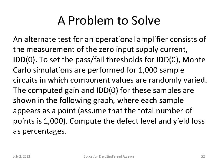
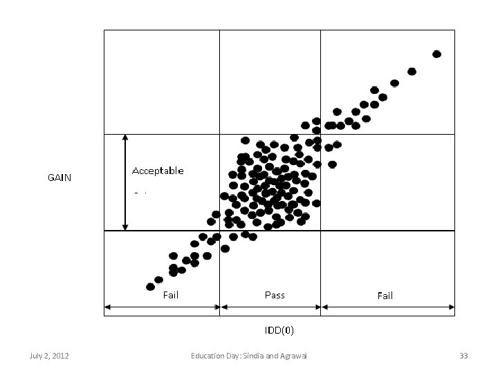
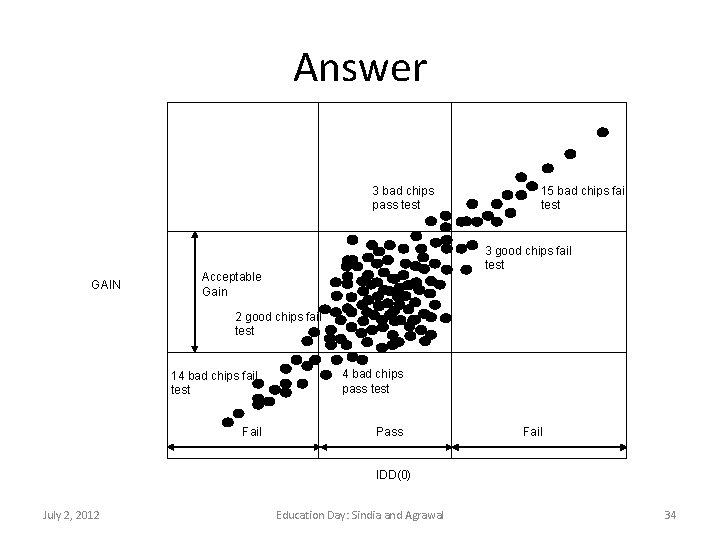
A Problem to Solve An alternate test for an operational amplifier consists of the measurement of the zero input supply current, IDD(0). To set the pass/fail thresholds for IDD(0), Monte Carlo simulations are performed for 1, 000 sample circuits in which component values are randomly varied. The computed gain and IDD(0) for these samples are shown in the following graph, where each sample appears as a point (assume that the total number of points is 1, 000). Compute the defect level and yield loss as percentages. July 2, 2012 Education Day: Sindia and Agrawal 32

July 2, 2012 Education Day: Sindia and Agrawal 33

Answer 3 bad chips pass test GAIN 15 bad chips fail test 3 good chips fail test Acceptable Gain 2 good chips fail test 14 bad chips fail test Fail 4 bad chips pass test Pass Fail IDD(0) July 2, 2012 Education Day: Sindia and Agrawal 34

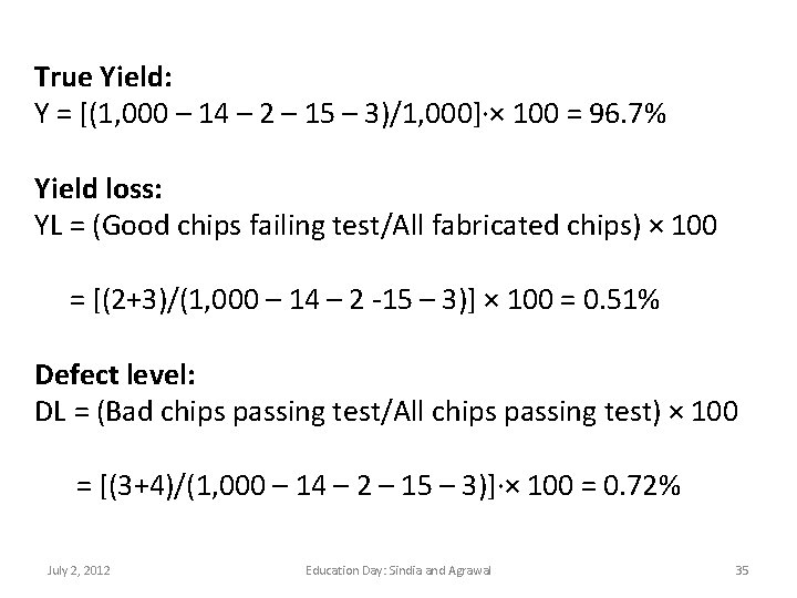
True Yield: Y = [(1, 000 – 14 – 2 – 15 – 3)/1, 000]·× 100 = 96. 7% Yield loss: YL = (Good chips failing test/All fabricated chips) × 100 = [(2+3)/(1, 000 – 14 – 2 -15 – 3)] × 100 = 0. 51% Defect level: DL = (Bad chips passing test/All chips passing test) × 100 = [(3+4)/(1, 000 – 14 – 2 – 15 – 3)]·× 100 = 0. 72% July 2, 2012 Education Day: Sindia and Agrawal 35

References – Analog Test • A. Afshar, Principles of Semiconductor Network Testing, Boston: Butterworth-Heinemann, 1995. • M. Burns and G. Roberts, Introduction to Mixed-Signal IC Test and Measurement, New York: Oxford University Press, 2000. • M. L. Bushnell and V. D. Agrawal, Essentials of Electronic Testing for Digital, Memory and Mixed-Signal VLSI Circuits, Boston: Springer, 2000. • R. W. Liu, editor, Testing and Diagnosis of Analog Circuits and Systems, New York: Van Nostrand Reinhold, 1991. • M. Mahoney, DSP-Based Testing of Analog and Mixed-Signal Circuits, Los Alamitos, California: IEEE Computer Society Press, 1987. • A. Osseiran, Analog and Mixed-Signal Boundary Scan, Boston: Springer, 1999. • T. Ozawa, editor, Analog Methods for Computer-Aided Circuit Analysis and Diagnosis, New York: Marcel Dekker, 1988. • B. Vinnakota, editor, Analog and Mixed-Signal Test, Upper Saddle River, New Jersey: Prentice-Hall PTR, 1998. July 2, 2012 Education Day: Sindia and Agrawal 36

References – RF Test 1. S. Bhattacharya and A. Chatterjee, "RF Testing, " Chapter 16, pages 745 -789, in System on Chip Test Architectures, edited by L. -T. Wang, C. E. Stroud and N. A. Touba, Amsterdam: Morgan-Kaufman, 2008. 2. M. L. Bushnell and V. D. Agrawal, Essentials of Electronic Testing for Digital, Memory & Mixed-Signal VLSI Circuits, Boston: Springer, 2000. 3. J. Kelly and M. Engelhardt, Advanced Production Testing of RF, So. C, and Si. P Devices, Boston: Artech House, 2007. 4. B. Razavi, RF Microelectronics, Upper Saddle River, New Jersey: Prentice Hall PTR, 1998. 5. J. Rogers, C. Plett and F. Dai, Integrated Circuit Design for High-Speed Frequency Synthesis, Boston: Artech House, 2006. 6. K. B. Schaub and J. Kelly, Production Testing of RF and System-on-a-chip Devices for Wireless Communications, Boston: Artech House, 2004. July 2, 2012 Education Day: Sindia and Agrawal 37

References – Alternate Test • P. N. Variyam, S. Cherubal and A. Chatterjee, “Prediction of Analog Performance Parameters Using Fast Transient Testing, ” IEEE Trans. Computer-Aided Design, vol. 21, no. 3, pp. 349361, March 2002. • H. -G. Stratigopoulos and Y. Makris, “Error Moderation in Low-Cost Machine-Learning-Based Analog/RF Testing, ” IEEE Trans. Computer-Aided Design, vol. 27, no. 2, pp. 339 -351, February 2008. July 2, 2012 Education Day: Sindia and Agrawal 38