VLSI Testing Lecture 11 Analog Test Analog circuits
- Slides: 24

VLSI Testing Lecture 11: Analog Test § Analog circuits § Analog circuit test methods § Specification-based testing § Direct measurement § DSP-based testing § Fault model based testing § IEEE 1149. 4 analog test bus standard § Summary § References Copyright 2005, Agrawal & Bushnell Lecture 11: Analog Test 1

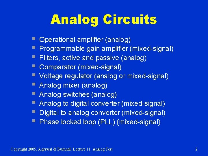
Analog Circuits § § § § § Operational amplifier (analog) Programmable gain amplifier (mixed-signal) Filters, active and passive (analog) Comparator (mixed-signal) Voltage regulator (analog or mixed-signal) Analog mixer (analog) Analog switches (analog) Analog to digital converter (mixed-signal) Digital to analog converter (mixed-signal) Phase locked loop (PLL) (mixed-signal) Copyright 2005, Agrawal & Bushnell Lecture 11: Analog Test 2

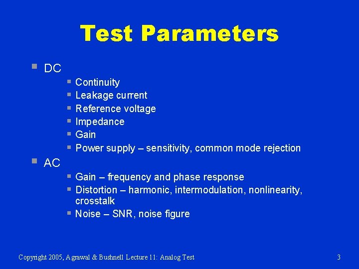
Test Parameters § DC § AC § Continuity § Leakage current § Reference voltage § Impedance § Gain § Power supply – sensitivity, common mode rejection § Gain – frequency and phase response § Distortion – harmonic, intermodulation, nonlinearity, § crosstalk Noise – SNR, noise figure Copyright 2005, Agrawal & Bushnell Lecture 11: Analog Test 3

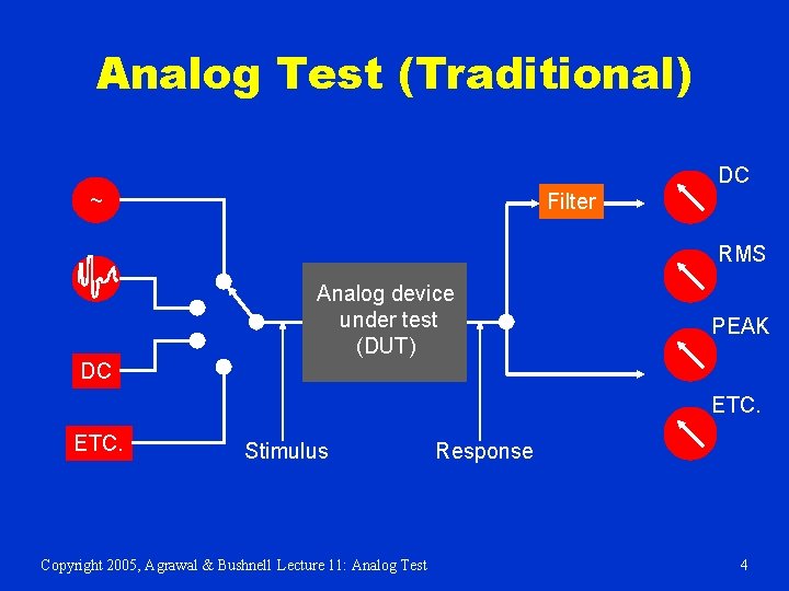
Analog Test (Traditional) DC ~ Filter RMS Analog device under test (DUT) PEAK DC ETC. Stimulus Copyright 2005, Agrawal & Bushnell Lecture 11: Analog Test Response 4

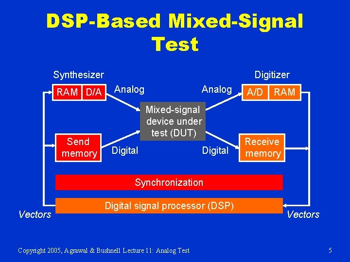
DSP-Based Mixed-Signal Test Synthesizer RAM D/A Send memory Digitizer Analog A/D Digital Receive memory Mixed-signal device under test (DUT) Digital RAM Synchronization Vectors Digital signal processor (DSP) Copyright 2005, Agrawal & Bushnell Lecture 11: Analog Test Vectors 5

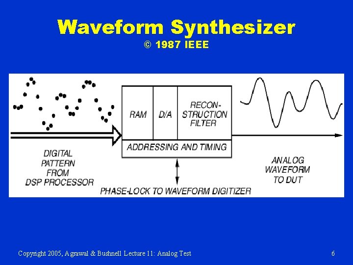
Waveform Synthesizer © 1987 IEEE Copyright 2005, Agrawal & Bushnell Lecture 11: Analog Test 6

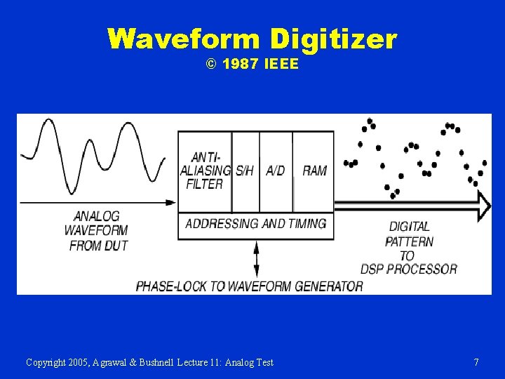
Waveform Digitizer © 1987 IEEE Copyright 2005, Agrawal & Bushnell Lecture 11: Analog Test 7

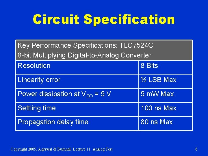
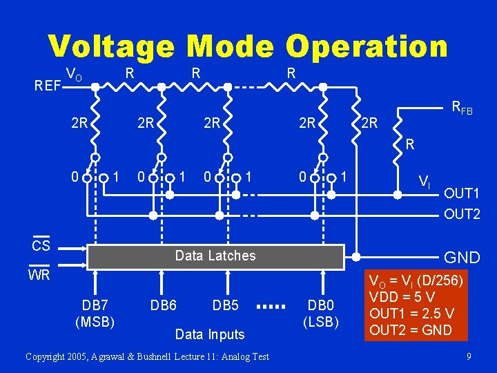
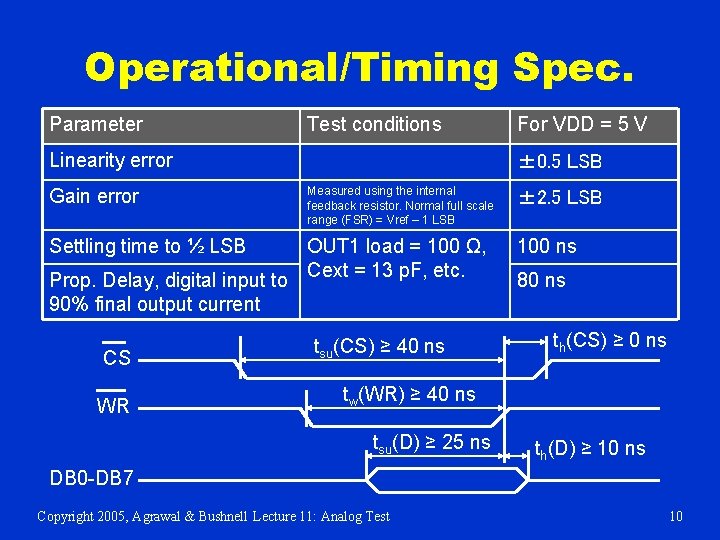
Circuit Specification Key Performance Specifications: TLC 7524 C 8 -bit Multiplying Digital-to-Analog Converter Resolution 8 Bits Linearity error ½ LSB Max Power dissipation at VDD = 5 V 5 m. W Max Settling time 100 ns Max Propagation delay time 80 ns Max Copyright 2005, Agrawal & Bushnell Lecture 11: Analog Test 8

Voltage Mode Operation REF VO R 2 R 2 R RFB 2 R R 0 1 CS 0 1 0 Data Latches DB 6 DB 5 Data Inputs Copyright 2005, Agrawal & Bushnell Lecture 11: Analog Test VI OUT 1 OUT 2 GND WR DB 7 (MSB) 1 DB 0 (LSB) VO = VI (D/256) VDD = 5 V OUT 1 = 2. 5 V OUT 2 = GND 9

Operational/Timing Spec. Parameter Test conditions Linearity error Gain error ± 0. 5 LSB Measured using the internal feedback resistor. Normal full scale range (FSR) = Vref – 1 LSB Settling time to ½ LSB OUT 1 load = 100 Ω, Prop. Delay, digital input to Cext = 13 p. F, etc. 90% final output current CS WR For VDD = 5 V tsu(CS) ≥ 40 ns ± 2. 5 LSB 100 ns 80 ns th(CS) ≥ 0 ns tw(WR) ≥ 40 ns tsu(D) ≥ 25 ns th(D) ≥ 10 ns DB 0 -DB 7 Copyright 2005, Agrawal & Bushnell Lecture 11: Analog Test 10

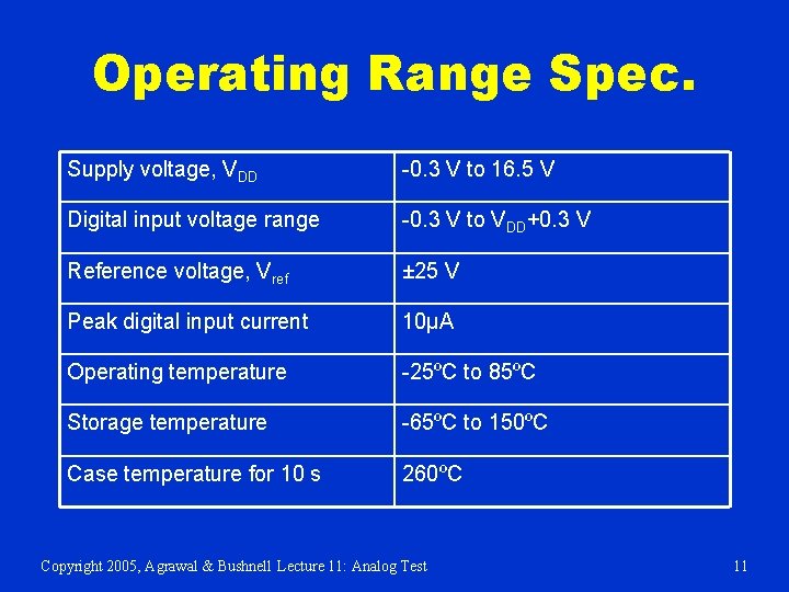
Operating Range Spec. Supply voltage, VDD -0. 3 V to 16. 5 V Digital input voltage range -0. 3 V to VDD+0. 3 V Reference voltage, Vref ± 25 V Peak digital input current 10μA Operating temperature -25ºC to 85ºC Storage temperature -65ºC to 150ºC Case temperature for 10 s 260ºC Copyright 2005, Agrawal & Bushnell Lecture 11: Analog Test 11

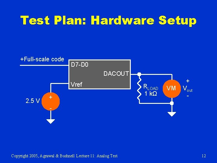
Test Plan: Hardware Setup +Full-scale code D 7 -D 0 DACOUT Vref 2. 5 V + RLOAD 1 kΩ VM + Vout - - Copyright 2005, Agrawal & Bushnell Lecture 11: Analog Test 12

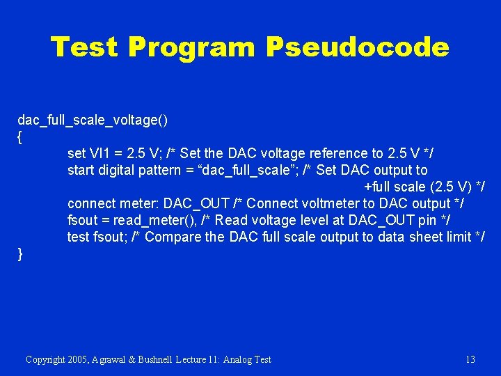
Test Program Pseudocode dac_full_scale_voltage() { set VI 1 = 2. 5 V; /* Set the DAC voltage reference to 2. 5 V */ start digital pattern = “dac_full_scale”; /* Set DAC output to +full scale (2. 5 V) */ connect meter: DAC_OUT /* Connect voltmeter to DAC output */ fsout = read_meter(), /* Read voltage level at DAC_OUT pin */ test fsout; /* Compare the DAC full scale output to data sheet limit */ } Copyright 2005, Agrawal & Bushnell Lecture 11: Analog Test 13

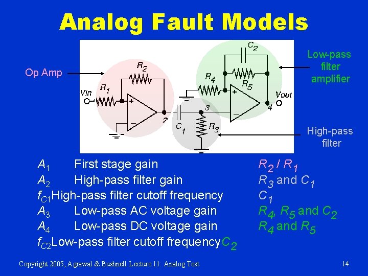
Analog Fault Models Op Amp Low-pass filter amplifier High-pass filter A 1 First stage gain A 2 High-pass filter gain f. C 1 High-pass filter cutoff frequency A 3 Low-pass AC voltage gain A 4 Low-pass DC voltage gain f. C 2 Low-pass filter cutoff frequency. C 2 Copyright 2005, Agrawal & Bushnell Lecture 11: Analog Test R 2 / R 1 R 3 and C 1 R 4, R 5 and C 2 R 4 and R 5 14

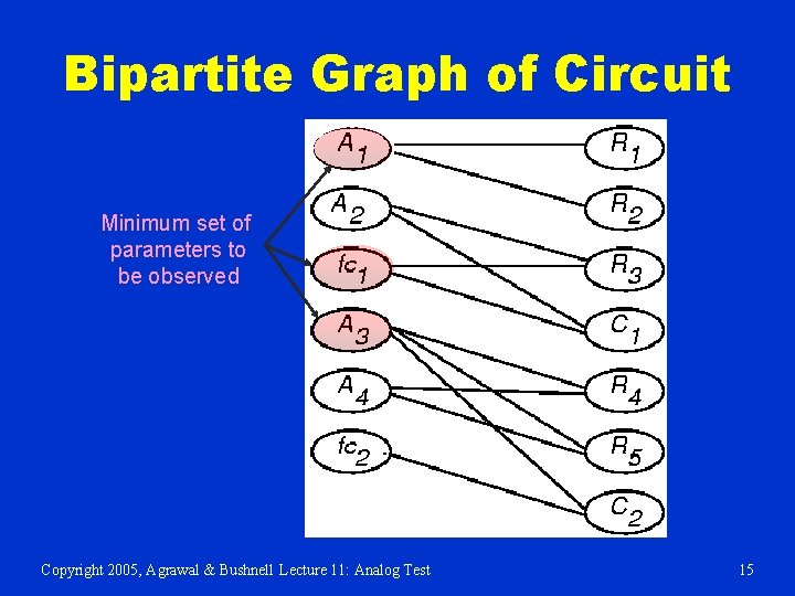
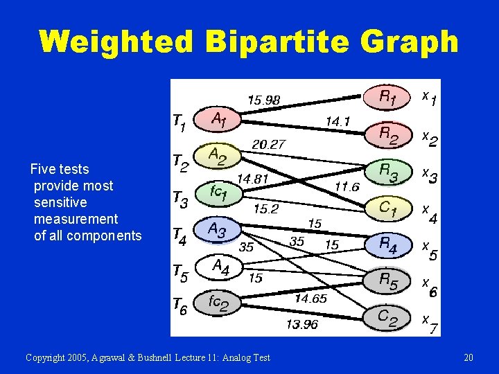
Bipartite Graph of Circuit Minimum set of parameters to be observed Copyright 2005, Agrawal & Bushnell Lecture 11: Analog Test 15

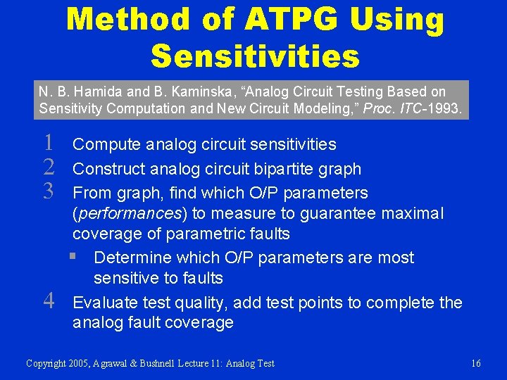
Method of ATPG Using Sensitivities N. B. Hamida and B. Kaminska, “Analog Circuit Testing Based on Sensitivity Computation and New Circuit Modeling, ” Proc. ITC-1993. 1 2 3 4 Compute analog circuit sensitivities Construct analog circuit bipartite graph From graph, find which O/P parameters (performances) to measure to guarantee maximal coverage of parametric faults § Determine which O/P parameters are most sensitive to faults Evaluate test quality, add test points to complete the analog fault coverage Copyright 2005, Agrawal & Bushnell Lecture 11: Analog Test 16

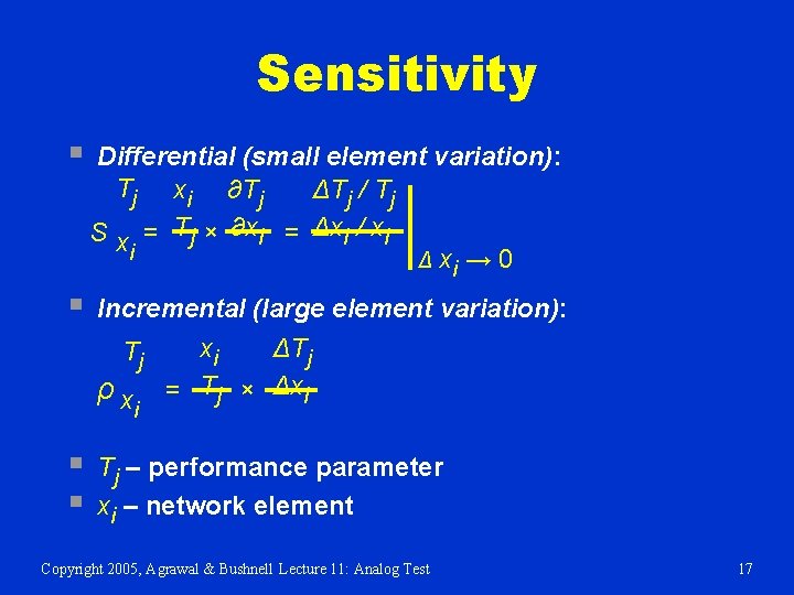
Sensitivity § Differential (small element variation): Tj xi ∂Tj ΔTj / Tj S x = Tj × ∂xi = Δxi / xi i Δ xi → 0 § Incremental (large element variation): Tj ρx i § § xi ΔTj = Tj × Δxi Tj – performance parameter xi – network element Copyright 2005, Agrawal & Bushnell Lecture 11: Analog Test 17

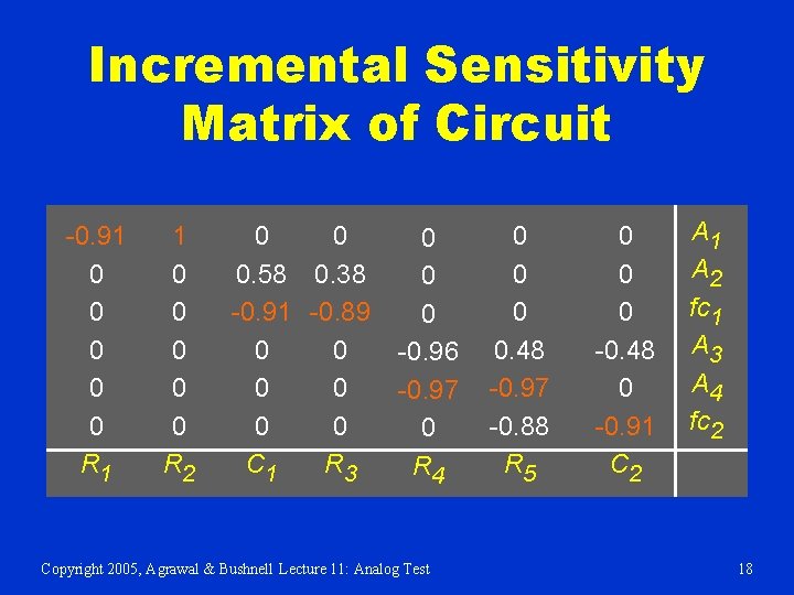
Incremental Sensitivity Matrix of Circuit -0. 91 0 0 0 R 1 1 0 0 0 R 2 0 0 0. 58 0. 38 -0. 91 -0. 89 0 0 0 C 1 R 3 0 0 0 -0. 96 -0. 97 0 R 4 Copyright 2005, Agrawal & Bushnell Lecture 11: Analog Test 0 0. 48 -0. 97 -0. 88 R 5 0 0 0 -0. 48 0 -0. 91 C 2 A 1 A 2 fc 1 A 3 A 4 fc 2 18

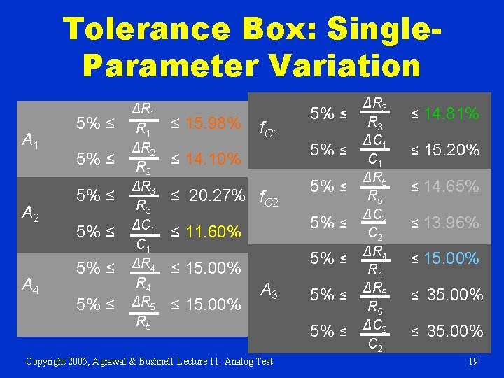
Tolerance Box: Single. Parameter Variation A 1 A 2 A 4 5% ≤ 5% ≤ ΔR 1 ΔR 2 ΔR 3 ΔC 1 ΔR 4 ΔR 5 ≤ 15. 98% f. C 1 5% ≤ ≤ 14. 10% ≤ 20. 27% f. C 2 5% ≤ ≤ 11. 60% 5% ≤ ≤ 15. 00% 5% ≤ A 3 Copyright 2005, Agrawal & Bushnell Lecture 11: Analog Test 5% ≤ ΔR 3 ΔC 1 ΔR 5 ΔC 2 ΔR 4 ΔR 5 ΔC 2 ≤ 14. 81% ≤ 15. 20% ≤ 14. 65% ≤ 13. 96% ≤ 15. 00% ≤ 35. 00% 19

Weighted Bipartite Graph Five tests provide most sensitive measurement of all components Copyright 2005, Agrawal & Bushnell Lecture 11: Analog Test 20

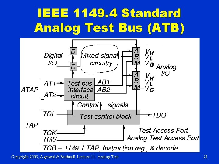
IEEE 1149. 4 Standard Analog Test Bus (ATB) Copyright 2005, Agrawal & Bushnell Lecture 11: Analog Test 21

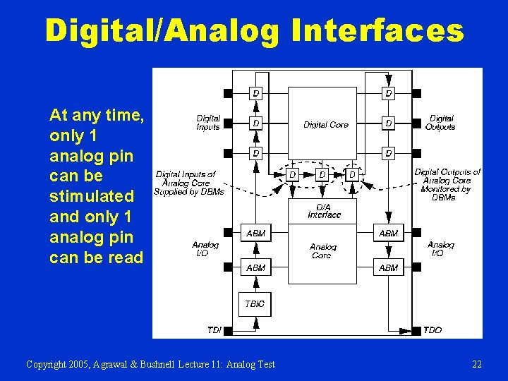
Digital/Analog Interfaces At any time, only 1 analog pin can be stimulated and only 1 analog pin can be read Copyright 2005, Agrawal & Bushnell Lecture 11: Analog Test 22

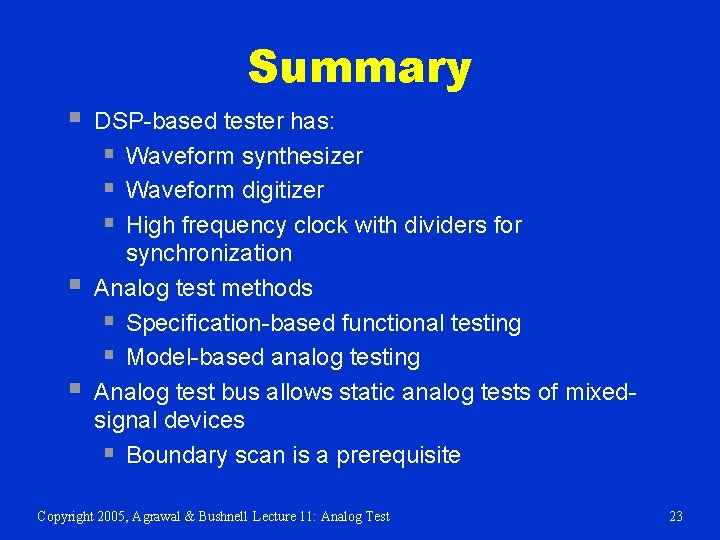
Summary § § § DSP-based tester has: § Waveform synthesizer § Waveform digitizer § High frequency clock with dividers for synchronization Analog test methods § Specification-based functional testing § Model-based analog testing Analog test bus allows static analog tests of mixedsignal devices § Boundary scan is a prerequisite Copyright 2005, Agrawal & Bushnell Lecture 11: Analog Test 23

References on Analog Test § § § § A. Afshar, Principles of Semiconductor Network Testing, Boston: Butterworth-Heinemann, 1995. M. Burns and G. Roberts, Introduction to Mixed-Signal IC Test and Measurement, New York: Oxford University Press, 2000. M. L. Bushnell and V. D. Agrawal, Essentials of Electronic Testing for Digital, Memory and Mixed-Signal VLSI Circuits, Boston: Springer, 2000. R. W. Liu, editor, Testing and Diagnosis of Analog Circuits and Systems, New York: Van Nostrand Reinhold, 1991. M. Mahoney, DSP-Based Testing of Analog and Mixed-Signal Circuits, Los Alamitos, California: IEEE Computer Society Press, 1987. A. Osseiran, Analog and Mixed-Signal Boundary Scan, Boston: Springer, 1999. T. Ozawa, editor, Analog Methods for Computer-Aided Circuit Analysis and Diagnosis, New York: Marcel Dekker, 1988. B. Vinnakota, editor, Analog and Mixed-Signal Test, Upper Saddle River, New Jersey: Prentice-Hall PTR, 1998. Copyright 2005, Agrawal & Bushnell Lecture 11: Analog Test 24