Analog Channel Testing n Overview Types of Analog

- Slides: 60

Analog Channel Testing

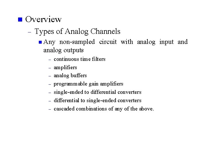
n Overview – Types of Analog Channels n Any non-sampled circuit with analog input and analog outputs – – – – continuous time filters amplifiers analog buffers programmable gain amplifiers single-ended to differential converters differential to single-ended converters cascaded combinations of any of the above.

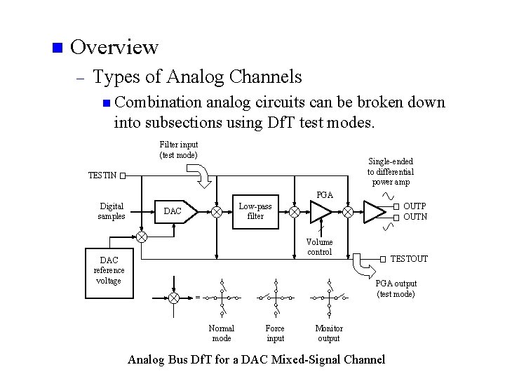
n Overview – Types of Analog Channels n Combination analog circuits can be broken down into subsections using Df. T test modes. Filter input (test mode) Single-ended to differential power amp TESTIN PGA Digital samples Low-pass filter DAC OUTP OUTN Volume control DAC reference voltage TESTOUT PGA output (test mode) = Normal mode Force input Monitor output Analog Bus Df. T for a DAC Mixed-Signal Channel

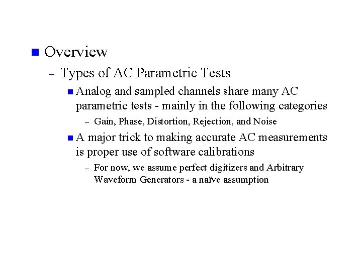
n Overview – Types of AC Parametric Tests n Analog and sampled channels share many AC parametric tests - mainly in the following categories – Gain, Phase, Distortion, Rejection, and Noise n. A major trick to making accurate AC measurements is proper use of software calibrations – For now, we assume perfect digitizers and Arbitrary Waveform Generators - a naïve assumption

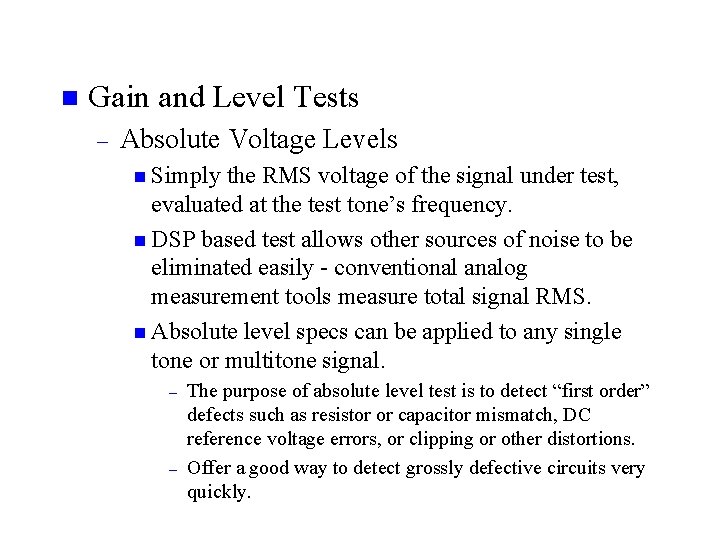
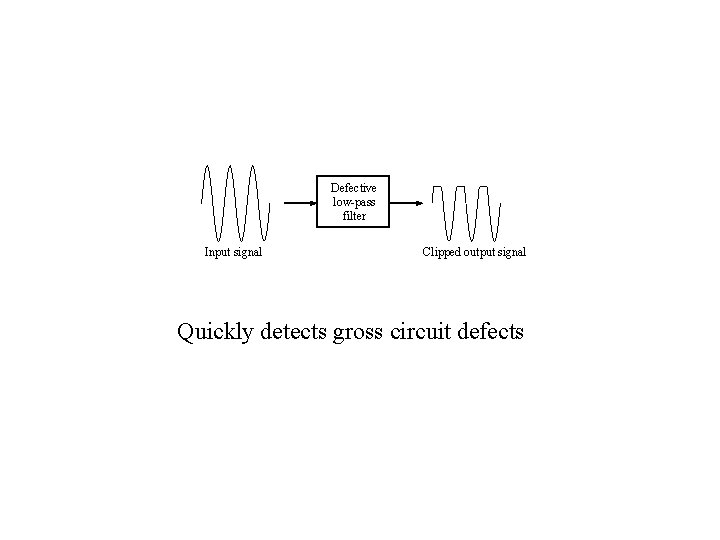
n Gain and Level Tests – Absolute Voltage Levels n Simply the RMS voltage of the signal under test, evaluated at the test tone’s frequency. n DSP based test allows other sources of noise to be eliminated easily - conventional analog measurement tools measure total signal RMS. n Absolute level specs can be applied to any single tone or multitone signal. – – The purpose of absolute level test is to detect “first order” defects such as resistor or capacitor mismatch, DC reference voltage errors, or clipping or other distortions. Offer a good way to detect grossly defective circuits very quickly.

Defective low-pass filter Input signal Clipped output signal Quickly detects gross circuit defects

n Gain and Level Tests – Absolute Voltage Levels - cont. n Loading – – Test engineer’s job is to determine the worst case loading conditions for a given AC test. The load must be designed into the DIB. In most cases, the load must be removable so that tests like continuity and leakage can be performed. n Units – n In is critical in performance of AC circuits of measure are: RMS volts, peak Volts, peak-to-peak Volts, d. BV (decibels relative to 1. 0 Volt RMS) and d. Bm (decibels relative to 1. 0 m. W) ATE testers, absolute voltage levels are measured using a general purpose digitizer and DSP based testing

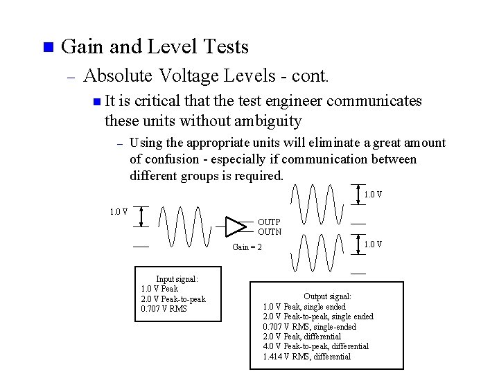
n Gain and Level Tests – Absolute Voltage Levels - cont. n It is critical that the test engineer communicates these units without ambiguity – Using the appropriate units will eliminate a great amount of confusion - especially if communication between different groups is required. 1. 0 V OUTP OUTN Gain = 2 Input signal: 1. 0 V Peak 2. 0 V Peak-to-peak 0. 707 V RMS 1. 0 V Output signal: 1. 0 V Peak, single ended 2. 0 V Peak-to-peak, single ended 0. 707 V RMS, single-ended 2. 0 V Peak, differential 4. 0 V Peak-to-peak, differential 1. 414 V RMS, differential

n Gain and Level Tests – Absolute Voltage Levels - cont. n Decibels – – – can be abused as well The decibel unit represents a ratio of values, and as such it is inappropriate to refer to an absolute voltage level using d. B without a reference level. Decibels is commonly referenced as d. BV or d. Bm A specified load impedance must be linked to the d. Bm specification

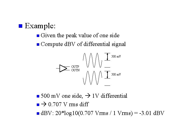
n Example: n Given the peak value of one side n Compute d. BV of differential signal 500 m. V OUTP OUTN 500 m. V one side, 1 V differential n 0. 707 V rms diff n d. BV: 20*log 10(0. 707 Vrms / 1 Vrms) = -3. 01 d. BV n 500

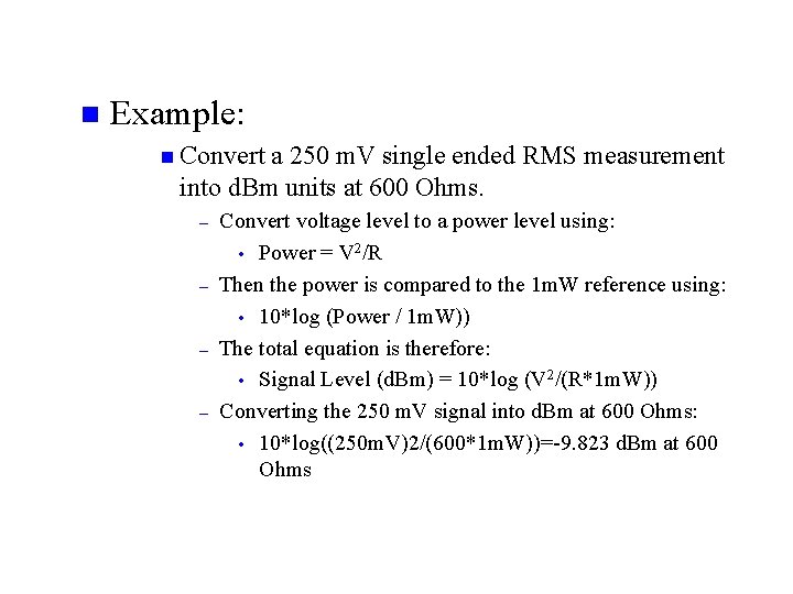
n Example: n Convert a 250 m. V single ended RMS measurement into d. Bm units at 600 Ohms. – – Convert voltage level to a power level using: • Power = V 2/R Then the power is compared to the 1 m. W reference using: • 10*log (Power / 1 m. W)) The total equation is therefore: • Signal Level (d. Bm) = 10*log (V 2/(R*1 m. W)) Converting the 250 m. V signal into d. Bm at 600 Ohms: • 10*log((250 m. V)2/(600*1 m. W))=-9. 823 d. Bm at 600 Ohms

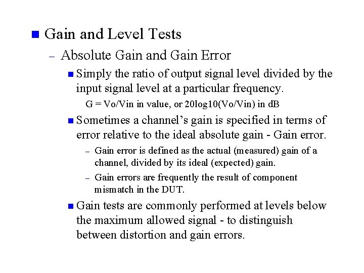
n Gain and Level Tests – Absolute Gain and Gain Error n Simply the ratio of output signal level divided by the input signal level at a particular frequency. G = Vo/Vin in value, or 20 log 10(Vo/Vin) in d. B n Sometimes a channel’s gain is specified in terms of error relative to the ideal absolute gain - Gain error. – – Gain error is defined as the actual (measured) gain of a channel, divided by its ideal (expected) gain. Gain errors are frequently the result of component mismatch in the DUT. n Gain tests are commonly performed at levels below the maximum allowed signal - to distinguish between distortion and gain errors.

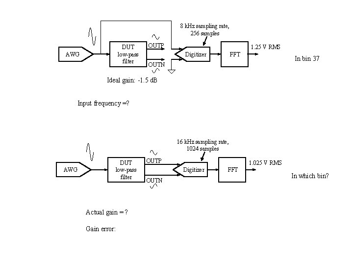
8 k. Hz sampling rate, 256 samples DUT low-pass filter AWG OUTP 1. 25 V RMS FFT Digitizer In bin 37 OUTN Ideal gain: -1. 5 d. B Input frequency =? 16 k. Hz sampling rate, 1024 samples AWG DUT low-pass filter Actual gain = ? Gain error: OUTP 1. 025 V RMS Digitizer OUTN FFT In which bin?

n Gain and Level Tests – Gain Tracking Error n The variation in the gain of a channel as the signal amplitude changes. – – Although a perfect analog circuit has no gain tracking error, small circuit defects can cause non-linearities in gain over changing input voltage. A major source of gain tracking error comes from quantization errors in DAC or ADC - usually most severe in low amplitude signals. Gain tracking is calculated by measuring the gain at a reference level. Gain tracking error is calculated at each signal level by subtracting the reference d. B from the measured gain at that level. Gain tracking error is specified in decibels.

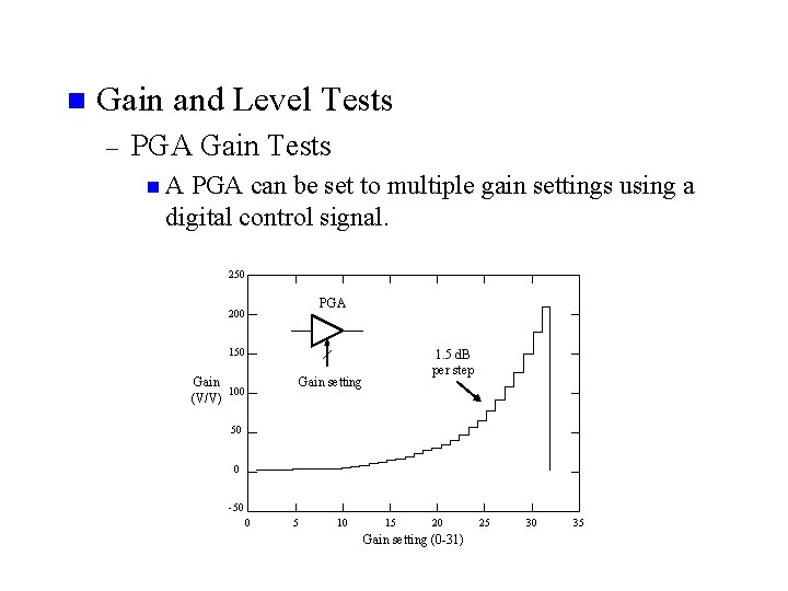
n Gain and Level Tests – PGA Gain Tests n. A PGA can be set to multiple gain settings using a digital control signal. 250 PGA 200 150 Gain 100 (V/V) 1. 5 d. B per step Gain setting 50 0 -50 0 5 10 15 20 Gain setting (0 -31) 25 30 35

n Gain and Level Tests – PGA Gain Tests n. A PGA can be set to multiple gain settings using a digital control signal. – – Usually used as a volume control in cellular telephones, televisions etc. PGAs are specified with an absolute gain at the first setting, a total gain difference between the highest and lowest setting, and the gain step size from each gain setting to the next. PGA specifications are usually tested at a particular frequency. The absolute gain, gain step size, and gain range can all be measured by setting the PGA into each of its gain settings and measuring the output voltage level divided by its input voltage level.

n Gain and Level Tests – PGA Gain Tests - cont. n Possible – – – measurement techniques: The absolute gain of each step can be measured by leaving the input signal unchanged and observing the output voltage. • This eliminates the need for a focussed calibration on the source Also, it is possible to adjust the input level at each step to produce a fairly constant output level at least 3 d. B lower than the full scale output to avoid clipping. • This produces a strong output signal level which is easier to measure. Finally, if the PGA is designed correctly, a binary weighted PGA allows six measurements to be made for a 32 step PGA, once superposition is verified in characterization.

n Gain and Level Tests – PGA Gain Tests - cont. n The – – question of superposition: How tight or loose are the test limits? • If the limits are loose, some error is tolerable and guardbanding can be used to insure the chip passes the gain test. Conclusions about superposition should be made from a fairly large set (statistically significant) of results not from a single chip.

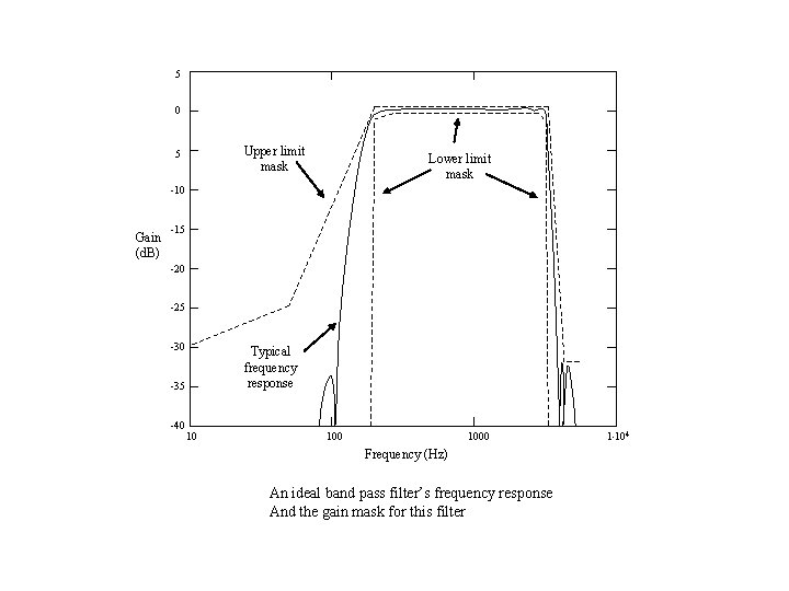
n Gain and Level Tests – Frequency Response n Similar to Gain tracking error, since it is a measurement of gain under varying signal conditions, relative to a reference gain. – – Usually used to measure the transfer curve of a filter Sometimes used to measure the bandwidth of a circuit • op amp to verify the gain bandwidth product. n Measures the variation in gain of the circuit as the signal frequency is varied. – One frequency is chosen as the reference gain, all other gains are measured relative to the reference. All nonreference gains are called relative gains.

5 0 Upper limit mask 5 Lower limit mask -10 Gain (d. B) -15 -20 -25 -30 Typical frequency response -35 -40 10 1000 Frequency (Hz) An ideal band pass filter’s frequency response And the gain mask for this filter 1 104

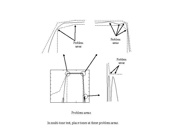
Problem areas In multi-tone test, place tones at these problem areas.

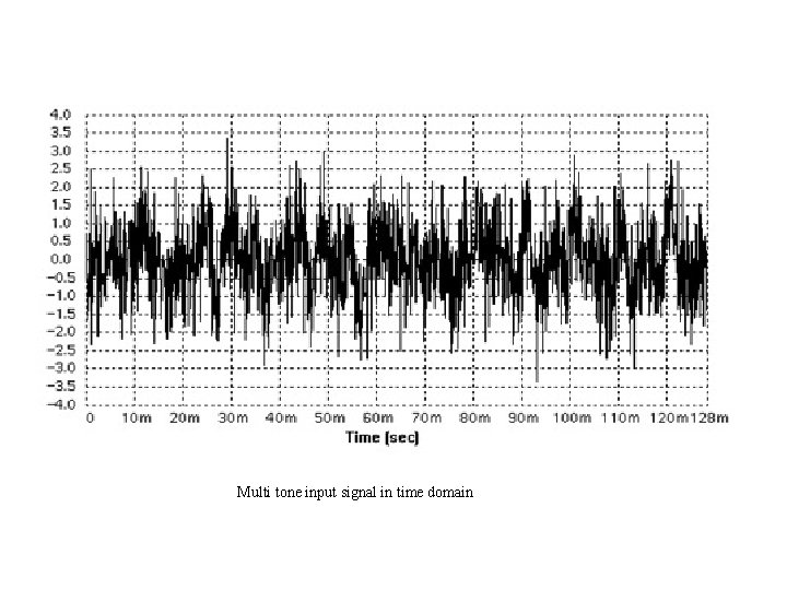
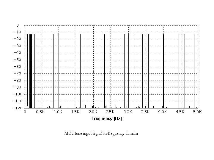
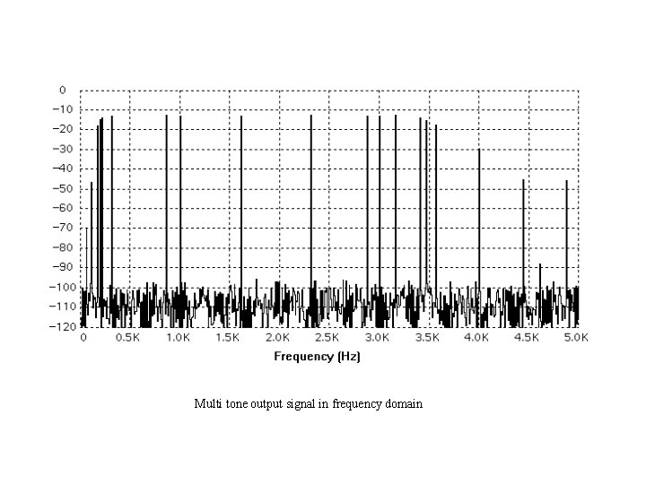
n Gain and Level Tests – Frequency Response - cont. n Frequency response is usually measured using a coherent equal-level multi-tone signal so that all signal frequencies can be measured simultaneously. – – Sometimes the test must be broken down into an in-band out-of-band test due to the large difference in signal amplitudes. • Out-of-band test requires an amplifier stage on the DIB to insure signal strength. Settling time of an AC system is determined by the characteristics of the DUT, AWG, Digitizer and Filters. • In general, the lower the frequency being tested, the longer the settling time.

Multi tone input signal in time domain

Multi tone input signal in frequency domain

Multi tone output signal in frequency domain

n Gain and Level Tests – Frequency Response - cont. n Using – – DSP, frequency response is easy to calculate: Perform a DFT or FFT on the waveform collected at the DUT input and output. Gain at each frequency is calculated The reference gain is the subtracted from each of the other gains to normalize them to the reference frequency gain. The absolute gain of the filter at the reference frequency is usually tested as a separate specification to guarantee the overall filter specification.

n Gain and Level Tests – Frequency Response - cont. n Frequency response can also be measured by applying a narrow impulse to the circuit under test and observing the filter’s impulse response. – – – The Fourier transform of the impulse response is the filter frequency response. The advantage is that this gives the full frequency response at all frequencies in the FFT spectrum. The problem with impulse response is that you can not measure the response at a particular frequency with any great accuracy. • Energy in a narrow impulse is very small - makes the measurement susceptible to noise • Also, frequency overlap and distortion may corrupt the gain at any single frequency.

HW Consider M-point multi-tone tests. Determine the minimum and maximum frequencies, and maximum number of frequencies that can be included. n For a high-gain op amp, how can its frequency response be tested efficiently? n

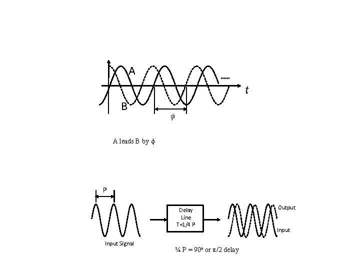
n Phase Tests – Phase Response n The transfer function of a circuit is defined not only by the magnitude information - it also can give the frequency or phase shift information - just like a Bode Plot. – – Phase can be obtained from either the exponential version of the DFT/FFT or from the sine/cosine pair coefficients. Please study the description of discrepancy in the phase calculation caused by notations given on page 365 Also, phase for a signal with negative sine and cosine components gives the same answer as phase with positive sine and cosine components (this is called wrap around) Finally, the phase calculation can not have zero in the denominator or it causes a singularity.

A t B A leads B by f P Delay Line T=1/4 P Input Signal ¼ P = 90 o or p/2 delay Output Input

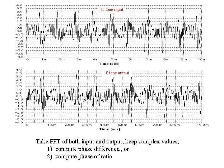
n Phase Tests – Phase Response - cont. n The phase shift in a multitone test signal is calculated by subtracting the input signal phase shift from the output signal phase shift, and then correcting for any wrap-around. n A negative phase shift indicates a positive time delay (i. e. the output lags the input), while a positive phase shift indicates the opposite. n Using multitone DSP, all phase shifts can be calculated from the same set of sampled data, reducing test time.

10 tone input 10 tone output Take FFT of both input and output, keep complex values, 1) compute phase difference. , or 2) compute phase of ratio

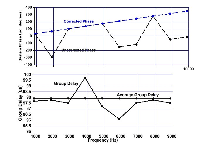
n Phase Tests – Group Delay n. A measurement of time shift versus frequency. n Defined as the change in phase shift divided by the change in frequency. – In reality it is extremely difficult to resolve tiny changes in phase. n Typically measured with tone pairs centered around the frequency of interest. n Multiple tone pairs can be measured simultaneously using DSP based Test techniques.

n Phase Tests – Group Delay Distortion n In a simple delay line, the phase shift is directly proportional to the frequency. – Indicated by a circuit that shifts each signal component by a constant amount of time. n If on the other hand, group delay varies over frequency, and the circuit shifts various signal components relative to one another, this results in a change in shape as well as a shift in time. This is called Group Delay Distortion. – This is important mainly in data communications, since phase carries important information, leading to corrupted data.

n Phase Tests – Group Delay Distortion - cont. n Group Delay is calculated by dividing the change in phase (degrees) between two test tones by the change in frequency (degrees per second). Leaving the units of seconds.


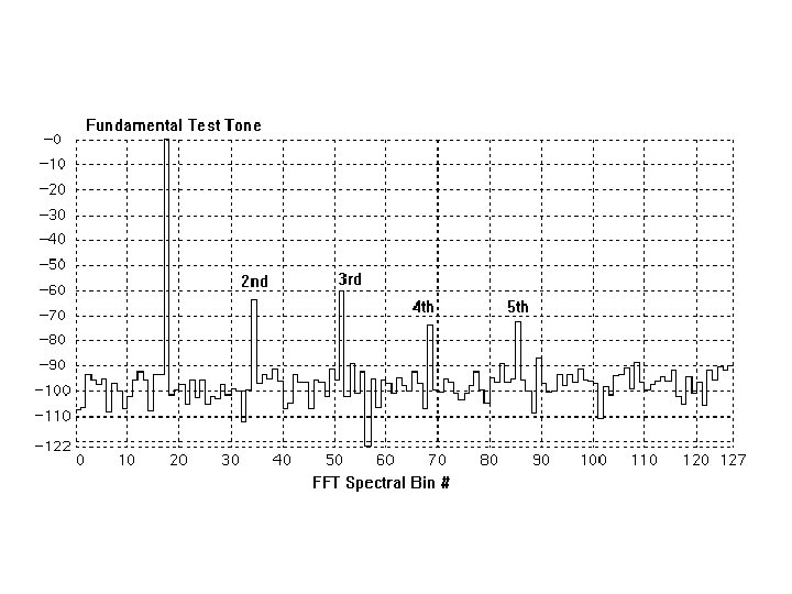
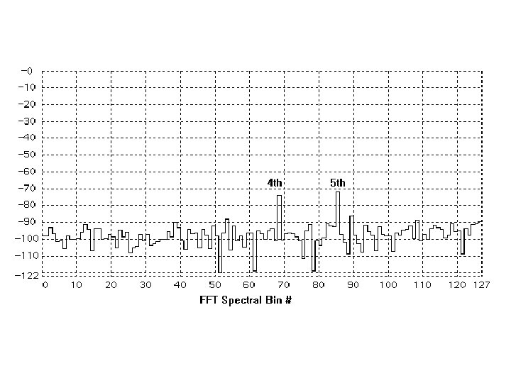
n Distortion Tests – Signal to Harmonic Distortion n Arises when a signal passes through a non-linear circuit – – to save test time, the distortion can be measured simultaneously with the gain using the FFT. when passing a single tone through a DUT, the harmonic distortion appears at integer multiples of the test tone, called harmonics. signal to total harmonic distortion is defined as the ratio of the RMS signal level of the test tone divided by the total RMS of the odd and even harmonic distortion components - expressed in d. B. the spec sheet usually calls for signal to 2 nd or 3 rd harmonic distortions tests as well as the total harmonic distortion

n Distortion Tests – Signal to Harmonic Distortion - cont. – – – Low distortion levels can be very time consuming to measure, especially if the value is close to the noise floor of the DUT or ATE tester. Solved by averaging a large number of samples with the ATE digitizer, causing long test times. Low levels of distortion are inherently very costly to test, especially when they are close to failing test limits.

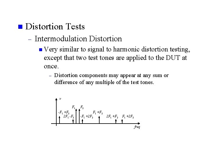
n Distortion Tests – Intermodulation Distortion n Very similar to signal to harmonic distortion testing, except that two test tones are applied to the DUT at once. – Distortion components may appear at any sum or difference of any multiple of the test tones. v F 1 -F 1 +F 2 2 F 1 -F 2 F 1 +F 2 -F 1 +2 F 2 2 F 1 +F 2 F 1 +2 F 2 freq

n Distortion Tests – Intermodulation Distortion n Intermodulation distortion is expressed as a ratio of the signal RMS of any one test tone to the signal RMS of the intermodulation components. – Usually with a limited number of intermodulation components given in the spec sheet.

n Distortion Test Definitions – Signal-to-Noise-Plus-Distortion (SNRD) n The ratio of the signal power to the total noise and distortion power from DC to the Nyquist frequency. DC is not counted as noise. The result is in d. Bs, and it is usually a positive number. – Total Harmonic Distortion (THD) n The ratio of the sum of the powers of nine harmonically related frequencies to the power of the signal frequency. The result is in d. Bs and it is usually a negative number. This number is an indication of nonlinearity (for instance in a DAC).

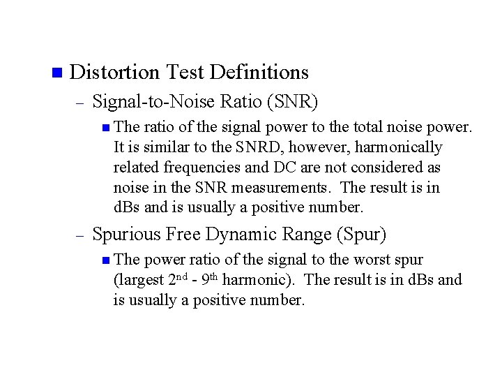
n Distortion Test Definitions – Signal-to-Noise Ratio (SNR) n The ratio of the signal power to the total noise power. It is similar to the SNRD, however, harmonically related frequencies and DC are not considered as noise in the SNR measurements. The result is in d. Bs and is usually a positive number. – Spurious Free Dynamic Range (Spur) n The power ratio of the signal to the worst spur (largest 2 nd - 9 th harmonic). The result is in d. Bs and is usually a positive number.

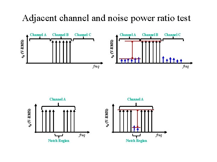
Adjacent channel and noise power ratio test Channel B Channel C Channel A Channel B Channel C ck (V-RMS) Channel A freq Channel A ck (V-RMS) Channel A freq Notch Region

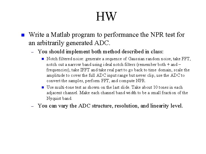
HW n Write a Matlab program to performance the NPR test for an arbitrarily generated ADC. – You should implement both method described in class: n n – Notch filtered noise: generate a sequence of Gaussian random noise, take FFT, notch out a narrow band using ideal notch filters (remember both + and – frequencies), take IFFT and take real part to go back to time domain, scale the amplitude to cover the full ADC input range but never clip, use the ADC to convert the samples, perform FFT, and compute NPR. Use multi-tone test as shown on the last slide. Take about 10 tones in each adjacent channel. Make each channel band width to be a small fraction of the Nyquist band. You can vary the ADC structure, resolution, and linearity level.

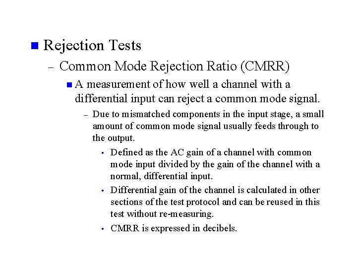
n Rejection Tests – Common Mode Rejection Ratio (CMRR) n. A measurement of how well a channel with a differential input can reject a common mode signal. – Due to mismatched components in the input stage, a small amount of common mode signal usually feeds through to the output. • Defined as the AC gain of a channel with common mode input divided by the gain of the channel with a normal, differential input. • Differential gain of the channel is calculated in other sections of the test protocol and can be reused in this test without re-measuring. • CMRR is expressed in decibels.

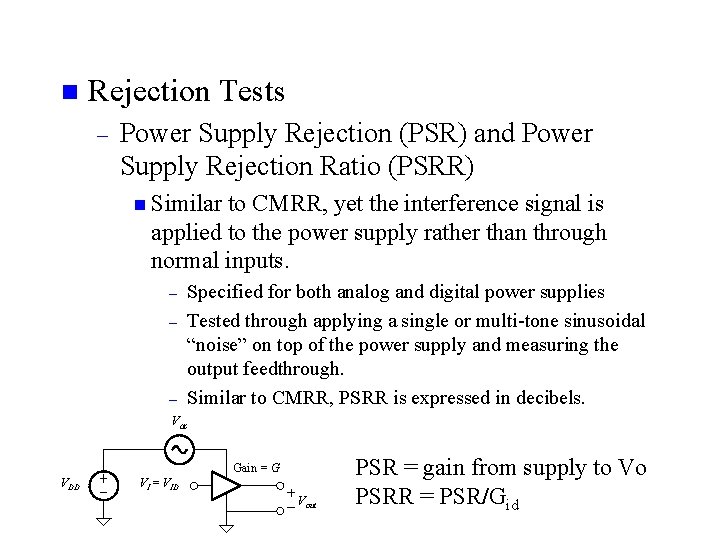
n Rejection Tests – Power Supply Rejection (PSR) and Power Supply Rejection Ratio (PSRR) n Similar to CMRR, yet the interference signal is applied to the power supply rather than through normal inputs. – – – Specified for both analog and digital power supplies Tested through applying a single or multi-tone sinusoidal “noise” on top of the power supply and measuring the output feedthrough. Similar to CMRR, PSRR is expressed in decibels. Vac Gain = G VDD VI = VID Vout PSR = gain from supply to Vo PSRR = PSR/Gid

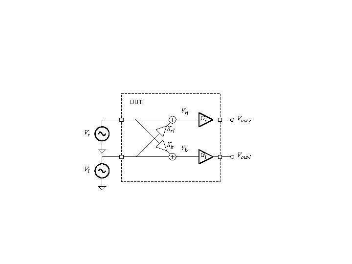
n Rejection Tests – Channel to Channel Crosstalk n Unlike CMRR and PSRR, crosstalk has no exact definition. – – Generally crosstalk is the gain from one channel to a second supposedly independent channel. In analog, crosstalk is defined as the gain from one channel’s input to another channels output, divided by the gain of the second channel. Nevertheless, the definition is vague, so the test engineer needs to be able to clarify the definition for each DUT. Crosstalk is measured at several frequencies using DSP based multi-tone testing.

DUT Vrl Vr Vout-r Gl Vout-l Xrl Xlr Vl Gr Vlr

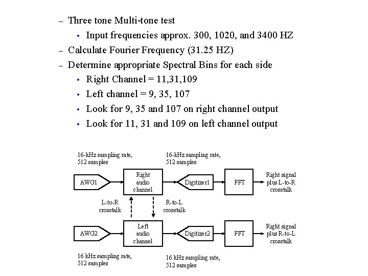
– – – Three tone Multi-tone test • Input frequencies approx. 300, 1020, and 3400 HZ Calculate Fourier Frequency (31. 25 HZ) Determine appropriate Spectral Bins for each side • Right Channel = 11, 31, 109 • Left channel = 9, 35, 107 • Look for 9, 35 and 107 on right channel output • Look for 11, 31 and 109 on left channel output 16 -k. Hz sampling rate, 512 samples Right audio channel AWG 1 L-to-R crosstalk AWG 2 16 k. Hz sampling rate, 512 samples Digitizer 1 FFT Right signal plus L-to-R crosstalk FFT Right signal plus R-to-L crosstalk Left audio channel Digitizer 2 16 k. Hz sampling rate, 512 samples

n Rejection Tests – Clock and Data Feedthrough n Another – very ambiguous term with no clear definition. Clock and data feedthrough is measured by digitizing the output of a channel and then applying one of several calculations on the resulting waveform. • Digital feedthrough has a very “spiky” appearance • Clock feedthrough often has a signal bandwidth well into the Megahertz range. • Specified in maximum spurious tone, relative to the carrier tone (d. Bc) • Also specified in terms of total RMS voltage, excluding the DC offset • Often it is not specified as a separate parameter - it is considered a part of the noise in a signal to noise test.

n Noise Tests – Noise n Noise – – – is generated by every real world circuit. Thermal noise (Johnson Noise) in resistors 1/f (Flicker Noise) in CMOS Quantization noise in DACs and ADCs Light falling onto a bare die electromagnetic interference n Noise is the leading contributor to long test times, due to averaging required to remove the nonrepeatability caused by random noise. n Spectral density is often referred to in terms of colors

n Noise Tests – Noise - cont. – – White noise, like white light has RMS voltage constant in any band of frequencies. Pink noise, by contrast, is noise that is weighted more heavily at low frequencies. Sometimes noise is defined as any signal component other than the primary test tone. This lumps all other distortions and noises into one measurement, which allows very limited debug-ability. A better solution is to identify all failure modes independently and test for each individually A combined Noise measurement can always be calculated as a measure of quality for the DUT from separate results.

n Noise Tests – Idle Channel Noise n. A measurement of the noise generated by the circuit itself, plus noise injected from external circuits or sources through a variety of coupling mechanisms. – – Inputs are usually shorted or grounded. Ideally, the output should be placed into low noise state. • Using DSP based testing, output noise is measured by digitizing the output of the circuit and performing a noise calculation on the captured samples. Idle channel noise can be expressed in many different units. • Simplest is to calculate the RMS voltage level from the captured samples

n Noise Tests – Idle Channel Noise - cont. – – It is important to remember that the bandwidth of the digitizer is extremely important - the larger the bandwidth, the larger the RMS of the noise, so it is critical to express the noise in terms of RMS voltage over a specified bandwidth. Idle channel noise is also specified in V/ Hz - the RMS voltage is divided by the square root of the frequency span of the bandwidth of the digitizer or voltmeter. - This number is referred to as the spectral density and allows back-calculation of the idle channel noise over a different bandwidth.

n Noise Tests – Signal to Noise and Distortion n Signal to noise ratio is another way to measure the noise in an analog or mixed-signal channel – – Different from idle channel noise in that it measures noise in the presence of a test signal, usually a sine wave. In a purely analog channel, this should not change the noise value - if an ADC or DAC are present, quantization noise is introduced into the calculation. Signal to noise ratio is often measured using the same data collected during the gain and signal to distortion tests. Defined as the ratio of the primary signal divided by all nonsignal components.

n Noise Tests – Spurious Free Dynamic Range n Spurious free dynamic range is a specification that is critical to audio circuits as well as telecom circuits that must pass FCC certifications. – A spur is defined as a noise component that is confined to a single frequency. • Caused by clock feedthrough, sigma-delta converter self tones, stray oscillations etc. • Spurs are much more noticeable by the human ear than other types of noise. • Also, spurs are mixed with transmitted signals in cellular phones which may interfere with calls on other cellular phones.

n Noise Tests – Spurious Free Dynamic Range - cont. n. A spur shows up on the FFT or on a spectrum analyzer as a spike in the frequency domain. n Spurious free dynamic range is defined as the difference in decibels between the 0 d. B signal level (the carrier level) and the maximum spur in the frequency domain.


n Weighting filters – Weighting filters can be applied to any FFT output before calculations are performed. – – – Usually designed to mimic the final application - like the human ear for cellular phones. • ANSI A-weighting filter • psophometric filter • C-message weighting filter Since the filters are only specified at certain frequencies, some interpolation is required - usually a straight line approximation on a log-log plot To save test time, weighted filter gain values should only be calculated once, during the first execution of the test program and stored for future use.